Wiznet W5300 Driver, Powered by Verilog HDL
Wiznet W5300 Driver, Powered by Verilog HDL
1
Components
Hardware components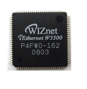
WIZnet - W5300
x 1

Project description
Wiznet W5300 Driver, Powered by Verilog HDL
Preface
W5300 is a TCP/IP controller, manufactured by WizNet Inc., which could be applied for Ethernet with TCP, UDP or PPPoE protocol based on IPv4.
This driver is planned to implement UDP communication in a LAN, with Intel Cyclone IV series. The FPGA chip is EP4CE10F17C8, with other hardware suites to debug or finish this design.
Why is Verilog HDL chosen, not VHDL or System Verilog? Well, the VHDL is too old to be applied in newer design. And the System Verilog is preferred but I use Verilog HDL and this design as my initial HDL development learning now.
Usage
This is a pure Quartus Prime project for Intel Cyclone IV series, but I think the key part, driver of W5300 is free to be ported to other platform.
The Quartus Prime used for this design is Quartus Prime Lite 22.1, and it is expected to be compatible for newer version of Quartus Prime Lite.
Restore project from TCL scripts
Open the "Tcl Console" from "View > Utility Window" menu in Quartus, and run following command:
source <absolute_path>/ethernet_w5300.tclThe project(.qpf, .qsf and other project files) would be restored in the root folder of this repo. Then it could be opened in Quartus.
Hardware
There are many hardware suite used, including UART, LEDs, keys, and W5300 itself. All pin allocation could be found in here, and it's used to restore whole Quartus Prime project, see here
Clock Source And Power Supplies
The Cyclone IV chip is driven by a 50MHz oscillator, and it is boosted up to 100MHz for W5300 interface. The core voltage supply for the chip itself is 1.2V, for IO banks is 3.3V, that means the the 3.3V LVTTL/LVCMOS is compatible for the chip.
The pin of oscillator input is E1, and the pin of the reset key is N13.
W5300 Suite
The W5300 I used is a individual board and it is connected to FPGA board by DuPont Lines. And there is a extra port to control bus tranceivers, which are used to isolate the W5300 and FPGA IOs.
W5300 is driven by a 25MHz oscillator, and the clock is boosted up to 150MHz in W5300 itself. 3.3V power supplies are preferred.
to be done: the pin allocation for w5300 suite.
LEDs
There are 4 LEDs, used as status indicator. LED0 blinks when FPGA is running normally in 500ms period. LED1 - LED3 indicate the error status of W5300.
| LED0 | LED1 | LED2 | LED3 |
|---|---|---|---|
| E10 | F9 | C9 | D9 |
The LEDs will light up when the IOs were put high level.
to be done: error list
UART
The UART is converted to USB interface by CP2102. And the driver clock of UART is 50MHz, default baud rate is 115200.
| TXD | RXD |
|---|---|
| N1 | M2 |
Others
The Signal Tap Logic Analyzer is enabled for W5300 interface debugging. It could be removed safely for saving resources of FPGA.
HDL Designs
W5300 LUTs
The interface of LUTs is familiar. They have a 6-bit input as operation index, and a 27-bit output data, which is composed by following:
- bit 26: 1 for reading and 0 for writing,
- bit 25-16: the address of w5300 register,
- bit 15-0: the data to be written or 0xFFFF for reading.
And an decleration of a LUT interface looks like this:
module _w5300_common_regs_conf_lut
(
    input [5:0] index,
    output reg [26:0] data
);

    // some content...

endmodule
There are some LUTs for most operations of Socket 0 of W5300 in UDP mode, see LUTs:
- configuration for common registers, e.g. MR, IMR, and registers of network configuration,
- configuration for Socket N,
- Tx/Rx operations,
- interrupt status reading & clearing.

