What components does a minimum system board require?
Easy for beginners to understand: a complete analysis of the Raspberry Pi Pico hardware circuit.
COMPONENTS
PROJECT DESCRIPTION
Beginners can think of the RP2040 chip as "a phone motherboard without a screen, battery or buttons" — it has core functions, but cannot work without these accessories. These hardware circuits supplement the chip with essential functions such as "power supply, clock generator, status indicator and interfaces", turning the Pico from a "bare chip" into a "directly usable development board".
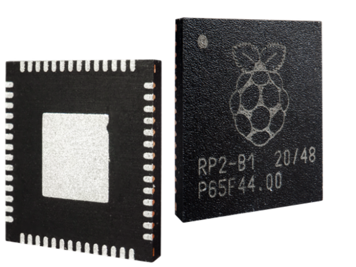
The Raspberry Pi Pico is equipped with some peripheral circuits of the RP2040 chip, including: an external Flash memory chip (W25Q16JV), a clock crystal oscillator, passive components such as power filter capacitors, a USB connector, a reset button, an LED indicator, etc. Most of the available pins of the RP2040 chip are led out on both sides of the Pico development board, and four pins are used for internal functions, including driving the onboard LED, powering the development board, and selecting the BOOT mode.
The schematic diagram of the Raspberry Pi Pico is shown below, which consists of an external clock crystal oscillator circuit, a BOOT mode selection circuit, a power supply input circuit, a power supply voltage measurement circuit, an LED indicator driving circuit, a debugging interface circuit, a pin expansion circuit and a chip peripheral circuit, and we will introduce them one by one next.
Figure 1.4 Circuit Schematic of Raspberry Pi Pico Development Board
Simply put, the peripheral circuits of a Pico development board consist of the following parts:
Clock Crystal Oscillator Circuit: A circuit composed of a 12MHz crystal oscillator (labeled X1 in the diagram) and small components such as capacitors. It acts as the "metronome" for the chip — the chip's operations and communication with peripherals all rely on precise "timing rhythm", and this circuit delivers a stable "beat signal" of 12 million cycles per second to ensure the chip operates with accurate timing (for example, timing a 1-millisecond LED flash relies entirely on this beat to calculate time).
BOOT Mode Selection Circuit: Essentially, it is a small circuit equipped with a BOOTSEL button, serving as the "boot mode toggle switch" for the chip, which has two modes upon startup:
Normal Mode: Launch the saved program;
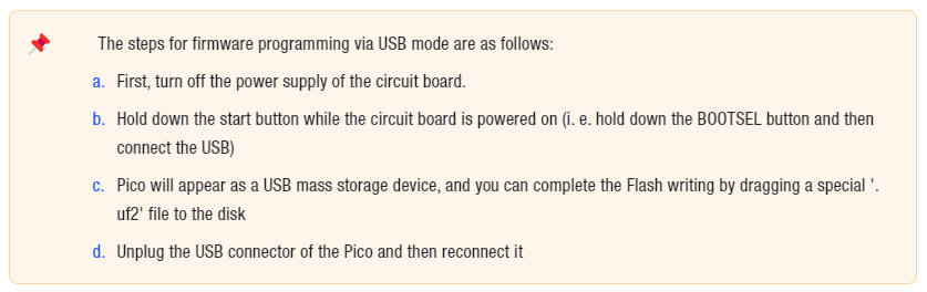
BOOT Mode: The firmware flashing state is the "program loading mode" of Pico: after connecting Pico to a computer while holding down the BOOTSEL button, Pico will switch to this state (without launching the old program). At this point, it will be recognized as a storage device by the computer, and you can add new functions to Pico by dragging the written program (firmware) into it.
Power supply input circuit: This is the circuit in charge of power management (such as the power chip U2 in the diagram). We can connect it to a USB (5V) power source or a battery (2-5V), and this circuit will stably convert the input voltage into the 3.3V required by the chips, as well as filter out the clutter in the voltage to prevent the chips from being burned out by fluctuating voltage.
Power Supply Voltage Measurement Circuit: A compact circuit designed to detect the power supply voltage. Acting as the "built-in voltmeter" of the board, it can measure the input power voltage in real time (for example, when powered by batteries, it lets you know if the batteries are running low), making it convenient for you to monitor the power status.
LED Indicator Driver Circuit: A small circuit for controlling the onboard LED. The chip can control the on/off state of this LED via the GPIO25 pin to indicate status (e. g., blinking when the program is running, steady-on when the power is connected).
Debug Interface Circuit: This refers to the DEBUG header (3-pin header) shown in the diagram, which serves as the "fault diagnosis port" of the board. If your program is corrupted or the board fails to operate, you can connect a debugging tool to this interface to check the internal operating status of the chip and pinpoint where the program has gone wrong.
Pin Extension Circuit: A circuit that converts the pins of a chip into header pins (labeled CON_PICO_40W in the diagram). The pins of the RP2040 chip are too small to connect wires directly; this circuit extends the chip's pins into header pins, allowing you to directly insert DuPont wires into these headers to connect external components such as sensors and motors.
Chip peripheral circuit: A circuit composed of small components such as filter capacitors and resistors around the chip. For example, filter capacitors can filter out the clutter in the power supply to make the power supply for the chip more stable; resistors can protect the pins from being burned out by excessive current, and prevent the chip from malfunctioning due to external interference or current fluctuations.
1. Power Supply Circuit
Figure 1.5 Schematic Diagram of Power Supply Circuit
The Raspberry Pi Pico can be powered by an external power supply or a Micro-USB cable, and there are two power lines worth our attention here:
VBUS line: This is the power supply from the microUSB bus, with a voltage of 5V. If the Raspberry Pi Pico is not powered via the microUSB connector, there will be no power input at this point.
VSYS Line: This is the power supply input line for the DC-DC power supply chip, with an input voltage range of 1.8~5.5V. The onboard RT6150B can convert the input power into + 3.3V voltage and output it to the MCU chip.
The entire power voltage conversion is completed by the RT6150B DC-DC power supply chip. The RT6150A/B is a high-efficiency, fixed-frequency switching power converter that operates from an input voltage that is higher than, lower than, or equal to the output voltage. This chip features low static power consumption (with a switching frequency set at 1MHz and a static current of only 60μA in the power-saving mode), compact size, selectable operating modes (with enable control for the power-saving mode PSM) and other advantages, and is commonly used in power supply modules for portable products and handheld instruments and meters.
Introduction to RT6150 Power Management IC
(1) Chip Parameters and Reference Circuit Design
Figure 1.6 Parameters and Reference Circuit Design of RT6150 Power Supply Chip
(2) PCB Routing Reference Diagram
Figure 1.7 PCB Routing Reference Diagram for RT6150 Power Supply Chip
Here, the GPIO23 pin of the Raspberry Pi Pico is connected to the PS pin of the power supply chip, and the operation mode of the power supply chip can be switched by controlling the high and low level output of GPIO23:
PS= 0: PFM (Pulse Frequency Modulation) mode, the default value, which delivers the optimal operating efficiency for the chip. This is the "high-efficiency power-saving mode" that ensures the power chip operates at peak efficiency during operation, making it fully sufficient for daily use.
PS= 1: The PWM (Pulse Width Modulation) mode refers to the "stable wave heavy-load mode", which delivers smoother power output and can drive heavier equipment; enabling this mode when using ADC (Analog-to-Digital Conversion) will yield more accurate data.
The RP2040 chip on the Raspberry Pi Pico requires two voltage supplies: 3.3V (for I/O) and 1.1V (for the digital core voltage of the chip). Since there is a built-in 3.3V-to-1.1V LDO inside the RP2040, there is no need to worry about the 1.1V power supply issue.
2. Clock Crystal Oscillator Circuit
Figure 1.8 Clock Crystal Oscillator Circuit
Chips cannot function without precise "timing rhythm" — for example, tasks like flashing an LED at 1-second intervals or transmitting data in sync with a sensor all rely on a stable "clock signal". This circuit acts as Pico's "external precision metronome", dedicated to providing a stable time reference for the RP2040. Below are its core components and their functions:
Here, a crystal oscillator in SMD3225-4P package with a frequency of 12MHz is selected. The 15pF capacitors on both sides of the crystal oscillator function to ensure more stable oscillation frequency, and a 1kΩ resistor connected in series in the XOUT path is used for current limiting, which can prevent the crystal oscillator from reduced service life or damage caused by over-driving. If other different crystal oscillators are selected, these values may need to be adjusted.
When strict timing requirements are not required, the clock of the RP2040 can be selected to be input from the internal oscillator.
3. BOOT Mode Selection Circuit
Figure 1.9 BOOT Mode Selection Circuit
This circuit comprises two key functional modules of the Pico: one is the BOOT mode selection circuit that controls the "startup state", and the other is the Flash memory circuit that stores programs — the former helps you switch between the states of "running the stored program" and "loading a new program", while the latter acts as the "built-in small hard drive" for the Pico to store programs. Their functions are detailed as follows:
The on-board 2MB QSPI flash memory can be (re-) programmed via the serial wire debug port or through a special USB mass storage device mode.
The upper part is the BOOT mode selection circuit. The startup mode switching button is connected in series with a 1kΩ resistor to the QSPI_SS pin of the RP2040. This series resistor ensures that the content in the Flash will be executed when the reset button is pressed in BootLoader mode.
When the RP2040 is powered on, the QSPI_SS pin will automatically default to a pull-up state. The RP2040 checks the value of this I/O during the boot process: if QSPI_SS is at logic 0, the RP2040 enters the BootLoader mode.
When the BOOTSEL button is not pressed, during reset or power-up: the device enters normal mode, and the MCU boots the stored program from the Flash.
When the BOOTSEL button is pressed during reset or power-up, the MCU enters the "program loading" BootLoader mode, at which point the Pico will appear as a "USB flash drive" on the connected computer; simply drag and drop a uf2 format program file to update the firmware.
During a short period at power-on, the state of the QSPI_SS pin cannot be guaranteed, which can be ensured by adding a pull-up resistor. For the W25Q128 Flash memory, an external pull-up resistor is unnecessary, so it is marked as NO-FIT and can be omitted during soldering.
The Flash memory circuit is located below; its power supply operates at the same voltage as the 3.3V power pin of the chip, and the pins of the W25Q128 are connected to the QSPIx pins of the RP2040. A 2.2μF filter capacitor and a 100nF filter capacitor are placed near the power supply pin (VCC) of the W25Q128 Flash memory to provide a stable 3.3V power supply for the W25Q128JVSIQ.
4. Power Supply Measurement Circuit
Figure 1.10 Power Supply Measurement Circuit
This circuit is the "power supply voltage monitoring module" of the Pico, which leverages the chip's ADC (analog signal acquisition) function to measure the Pico's supply voltage in real time (for example, to check the remaining battery level). First, let's understand the basics of the RP2040's ADC, then we will look at the function of this circuit:
The ADC of the RP2040 is a "tool for measuring gradual signals"(such as detecting voltage levels), and it has 5 acquisition channels:
The four channels correspond to the four pins GPIO26 to GPIO29;
One is the "temperature sensor" built into the chip, which can measure the chip's temperature without any external components;
There is also an ADC_VREF pin, which serves as the "reference standard" for ADC voltage measurement (by default it uses 3.3V, which determines the voltage range that the ADC can measure).
These ADC pins are internally protected by reverse diodes and feature a 12-bit resolution (equivalent to dividing the 0~3.3V range into 4096 small steps for more accurate voltage measurement).
The so-called power supply measurement circuit uses GPIO29 (corresponding to the ADC3 channel) to measure the supply voltage (VSYS) of the Pico:
C3 capacitor: Filters the voltage signal to stabilize the voltage to be measured and prevent clutter from interfering with the measurement results.
R5+ R6 Resistors: Divide the VSYS voltage (max. 5.5V) into 1/3 (since the ADC can only measure up to 3.3V, the divided voltage will fit the measurement range);
Q1 component: Prevents voltage from leaking into the power supply circuit from the ADC pin after the Pico is powered off, serving a protective function;
Finally, GPIO29 will collect the "divided VSYS voltage", and the current supply voltage can be obtained after conversion (for example, when powered by a battery, the battery level can be monitored).
5. Chip Peripheral Circuit
Figure 1.11 Peripheral Circuit of the Chip
The RP2040 chip serves as the "core brain" of the Pico, but it requires "supporting safeguards" to operate independently — the peripheral circuits below act as "auxiliary modules" that complement the chip with essential capabilities such as "communication, power supply, and anti-interference", enabling the chip to work stably and realize functions including USB connection and ADC acquisition, which are specifically divided into the following parts:
USB Communication Section: The two signal pins of the USB interface (USB_DP / USB_DM) must be connected to the USB interface in series with 27Ω resistors — these resistors function as "protection + optimizers": they not only prevent component burnout caused by excessive current during short circuits, but also enable smoother signal transmission and reduce interference, allowing the USB to be used both for firmware programming and for connecting external USB devices.
Chip Power Supply - Internal LDO Power Input: Inside the chip, there is a "voltage converter" that steps down 3.3V to 1.1V to power the core circuitry. The 2.2uF capacitors adjacent to its input and output pins act as "voltage regulators" to filter voltage fluctuations, ensure stable 1.1V power delivery, and prevent the chip from malfunctioning due to unstable voltage.
GPIO Peripheral Power Supply Input: The 100nF small capacitor next to the GPIO pin acts as an "anti-interference filter", which filters out the clutter in the power supply to make the GPIO pin more stable when powering external components or transmitting signals.
TESTEN: This is a pin for factory testing, which is directly connected to the ground wire and requires no attention from users.
ADC Reference Power Supply: By default, the ADC uses the Pico's built-in 3.3V as the "measurement reference" for voltage detection; for higher acquisition accuracy, a dedicated external voltage reference chip (such as the LM4040) can be connected, but in this case the ADC will only be able to measure voltages in the range of 0~3.0V.
ADC Power Supply - ADC_AVDD Pin: Supplies 3.3V power to the ADC module, using the stable 3.3V output from the preceding power management chip.
6. LED Driving Circuit
Figure 1.12 LED Driving Circuit
It is used to test the GPIO25 pin of the RP2040, and its on/off can be controlled via a program.
7. Debugging Interface Circuit
Figure 1.13 Debug Interface Circuit
This circuit serves as the 'program debug port' for the Pico — when the program you wrote malfunctions (for example, the board is unresponsive or functions incorrectly), it can help you troubleshoot issues and directly load code, making it more flexible than regular USB programming. Below is a breakdown of its specific functions:
There are two ways to reprogram Flash on Pico:
Normal mode: Drag and drop the uf2 file via USB (simple but with limited features);
This SWD debug port (DEBUG interface): It enables system reset, code loading/running, and "interactive debugging"(observing the internal operating status of the chip while the program is running to accurately locate program errors) without pressing any buttons.
Additionally:
The two debug pins SWDIO and SWCLK on the RP2040 chip come with a built-in 60kΩ pull-up resistor internally, so no additional resistor is required;
However, the more commonly used term in daily scenarios is "USB serial port debugging", which represents the most straightforward program download/debug method, and the USB approach is sufficient for most beginners.
8. Pin Expansion Circuit
Figure 1.14 Pin Expansion Circuit
The pins here are led out through 2 sets of "1×20Pin" stamp holes (each set has 20 pin holes), and the spacing between adjacent holes is 2.54mm — this is a common standard spacing for electronic components, compatible with regular DuPont wires and expansion boards.
The advantage of this design is its dual functionality: it can either be directly connected to components like sensors and LEDs via DuPont wires for experiments, or the Pico can be soldered onto a custom-designed circuit board, making it easy to integrate the Pico into your end products such as small robots and environmental monitoring devices.
9. Test Point Introduction
There are 6 test points (TP1 to TP6) accessible on the Raspberry Pi Pico:
Figure 1.15 Function Description Diagram of Test Points (TP1~TP6) for Raspberry Pi Pico
These 'test points (TP1~TP6)' are the reserved 'spare small interfaces' on the Pico board — normally, the main interfaces such as Micro-USB and pins are sufficient, but when you need to batch test whether the development board is functional, the main interface is damaged, or special operations are required, these test points can temporarily replace partial functions. The functions of each test point are as follows:
TP1, TP2, TP3: These are "spare USB ports" — if the Micro-USB port on the board is damaged, you can use these three test points to connect USB signals to replace the function of the original USB port;
TP4: Not intended for external use, ignore it;
TP5: Corresponds to GPIO25 (the pin of the onboard LED), but it is not recommended for use —— since its voltage can only vary between 0V and the LED turn-on voltage, which has an excessively narrow range, and using it as an output is prone to problems;
TP6: This is the "trigger point for the alternate BOOT mode". If the BOOTSEL button malfunctions, simply short TP6 to the ground line when powering on the device, and the Pico will enter the drag-and-drop programming mode for firmware flashing.