



Still confused about chip packaging?
Let's break down the differences between DIP, SOIC, QFP and BGA with RP2040!
COMPONENTS
PROJECT DESCRIPTION


What is "encapsulation"?
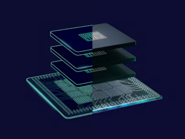
The core of a chip (the integrated circuit on the silicon wafer) can be understood as a "fragile bare die" — it is thin and delicate, vulnerable to impact and moisture, and has no directly connectable interfaces, making it impossible to use as-is. "Packaging" is the process of "fitting a protective casing and leading out interfaces" for this bare die:
It serves as the "protective casing" of a chip: it encloses the delicate core circuitry to resist impacts, moisture and dust, thereby preventing damage to the circuits.
It serves as the "external interface" of the chip: metal pins are drawn out from the core circuit to facilitate soldering the chip onto a circuit board, enabling the chip to receive power supply and transmit signals with external components.
Different packages feature varying shapes and pin counts. Take the "7×7mm QFN-56 package" used for the RP2040 as an example: QFN denotes the package type (a flat, no-lead form factor), 56 indicates that this package has 56 pins, and 7×7mm refers to the package's dimensions.
In addition to the QFN package used for the RP2040, here are other common chip packages:
DIP package (Dual In-line Package) Take "DIP-20" for example: its pins are long metal leads arranged in two rows, which can be directly inserted into a breadboard/perforated prototype board.
Features: beginner-friendly, easy to insert and solder, and easy to disassemble when damaged; however, it is relatively bulky.
Application scenarios: Experiments for beginners, prototype verification on breadboards (for example, early 51 single-chip microcontrollers commonly used DIP packages).
SOIC package (Small Outline Integrated Circuit package) For example, "SOIC-16": it is a surface-mount package, with pins being small metal leads on the surface of the circuit board, and its volume is much smaller than that of DIP.
Features: Compact size, suitable for tight-layout circuit boards; however, it requires surface-mount soldering, making manual soldering more difficult for beginners than DIP packages.
Application scenarios: Small consumer electronics (e. g., chips for Bluetooth modules, small-sized sensors).
QFP package (Quad Flat Package) Take "QFP-44" as an example: its pins are arranged on the four sides of the chip, and it has more pins than SOIC.
Features: It can support more functions (more pins correspond to more chip functions), with a size smaller than DIP but larger than BGA.
Applicable scenarios: Devices with medium complexity (such as some feature-rich microcontrollers and small industrial control board chips).
BGA package (Ball Grid Array package) For example, "BGA-100": its pins are solder balls on the bottom of the chip (not exposed pins), featuring an extremely compact size and a very large number of pins.
Features: It can accommodate a large number of pins (supporting high-performance chips) and has an extremely compact size; however, it requires professional equipment for soldering, making it hardly usable for beginners.
Application scenarios: High-end small devices (such as processors in mobile phones and tablets, high-performance sensor chips).
The core differences between these packages lie in their size, pin configuration, and soldering difficulty: DIP (easy to handle) is commonly used by beginners for experiments, SOIC/QFN is preferred for compact finished products, while BGA is adopted for high-end compact devices.
Documents
Comments
Write


