Embedded 101: RP2040 Core Voltage Regulator — Software Adjustable Modes for Low-Power Design
This article covers RP2040's on-chip core regulator, its adjustable voltage range, three operation modes, ROK indicator and configuration registers.
0
Project description
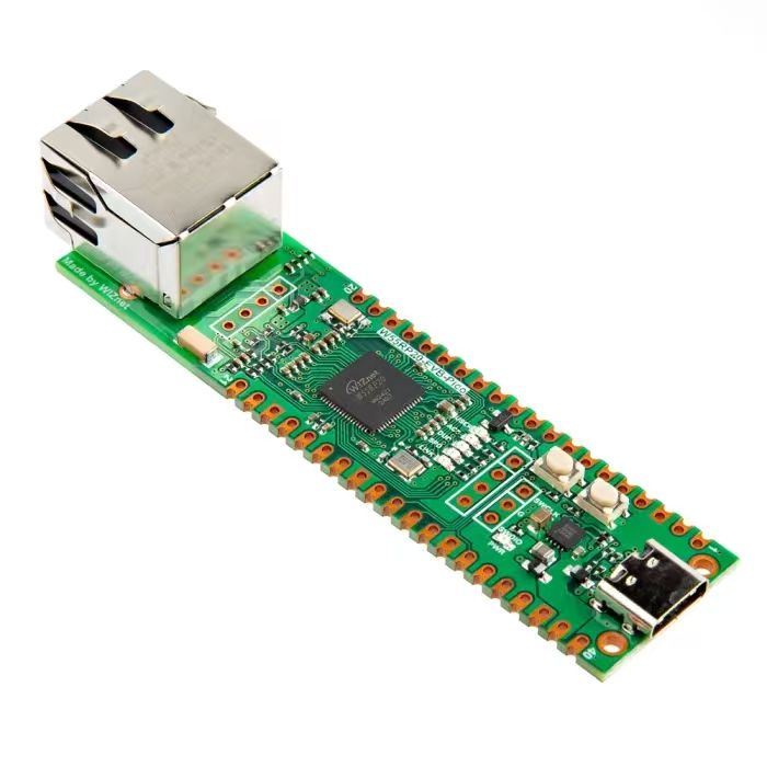
【Preliminary Note】The original hardware example in this article was written based on the RP2040. The actual hardware used in this hands-on demonstration features the W55RP20 as the main controller chip. The circuit logic and UF2 flashing operation principles are universally applicable, with only the main controller model differing. The original chip model mentioned in the circuit descriptions below is provided for reference purposes only.
Core Power Regulator
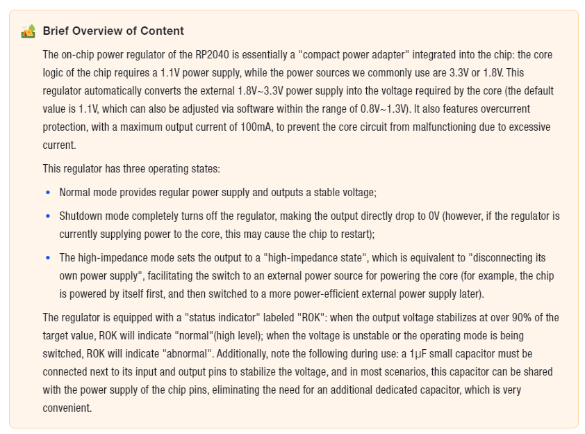
The RP2040 incorporates an on-chip core power regulator, which takes an external 1.8V~3.3V power supply as its input to power the DVDD digital core supply. In most scenarios, the input power supply for this regulator will share a single external source with the chip's digital IO supply, IOVDD, thereby simplifying the overall power requirements. To enable the chip to boot up, the voltage regulator is enabled by default and powers up as soon as the input supply is available. Once the chip exits reset, the regulator can be disabled and placed into a high-impedance state.
Its output voltage can also be adjusted under software control, which can be set within the range of 0.8V to 1.3V with a minimum adjustment step of 50mV. The default output voltage after initial power-on or reset is 1.1V, and the desired output voltage can be selected by writing to the VSEL field in the VREG register.
The voltage regulator incorporates a current limiter that caps the maximum output current at 100 mA to prevent the load current from exceeding the maximum rated value. When the current exceeds 100 mA, the output voltage will no longer be regulated and will drop below the set voltage value.
If DVDD is directly powered by an external power supply, the voltage regulator can be used elsewhere.
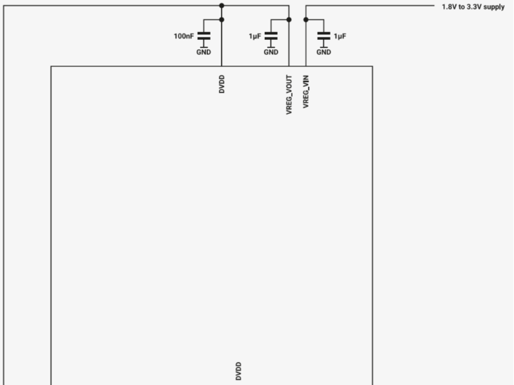
The common power supply scheme is shown in the following figure:
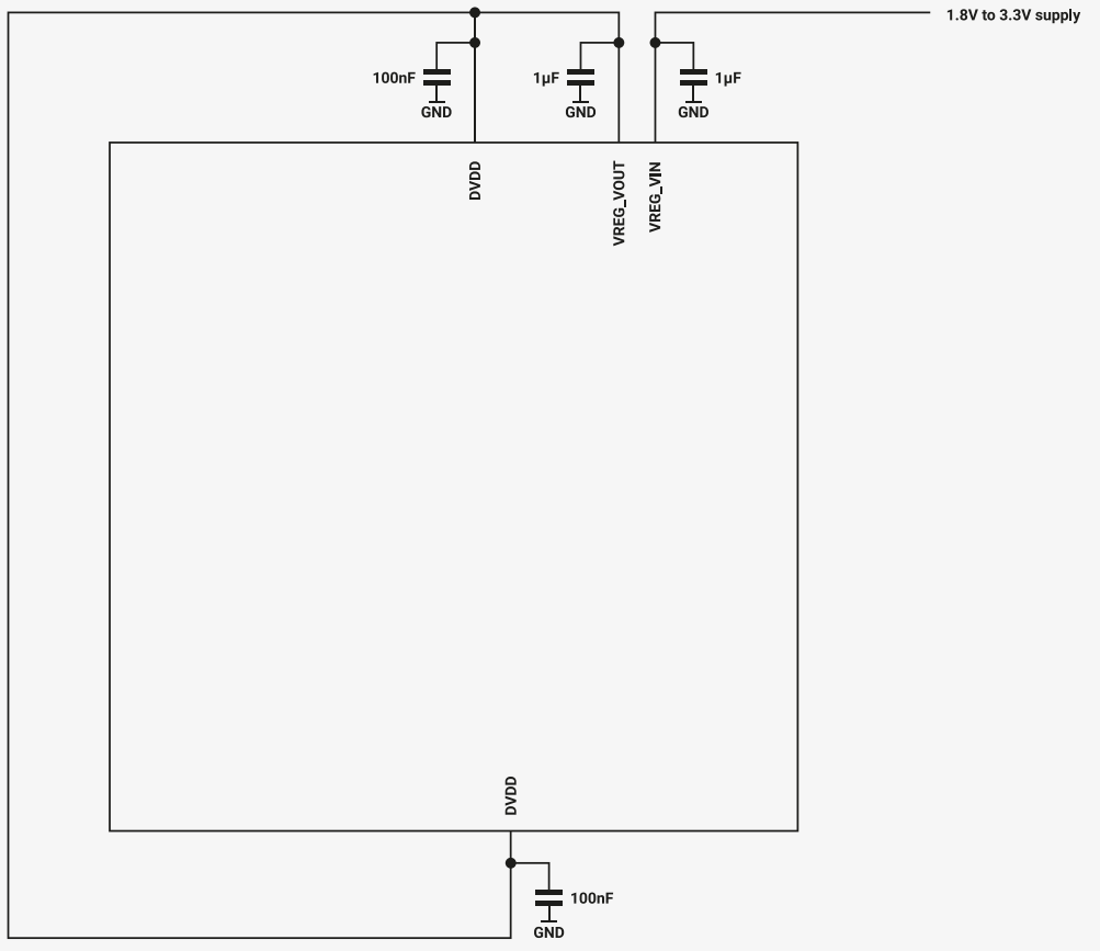
Schematic Diagram of RP2040 Core Power Regulator Power Supply and Capacitor Configuration (Figure 2.27)
The regulator must have a 1μF capacitor placed close to its input (VREG_VIN) and output (VREG_VOUT) pins.
1. Power Regulator Operating Mode
The on-chip voltage regulator operates in one of three modes. The mode to be used is selected by writing to the EN and HIZ fields in the VREG register, as shown in the table below. Upon initial power-up or after a reset event, the voltage regulator will be in the Normal Operation mode.

Table 2.28 RP2040 Power Regulator Operating Mode Configuration Table
The differences among the three operation modes are as follows:
Normal Operation Mode:
In normal operating mode, the output of the voltage regulator is regulated at the selected voltage, and the regulator is capable of supplying power
Shutdown Mode:
In shutdown mode, the voltage regulator is disabled, power consumption is minimized, and the regulator's output pin (VREG_VOUT) is pulled to 0V.
The shutdown mode is only useful when the voltage regulator does not supply power to the digital core (DVDD) of the RP2040.
When the regulator supplies DVDD:
If brown-out detection is enabled: entering shutdown mode will trigger a reset event, and the voltage regulator will return to normal mode
If brown-out detection is not used: the voltage regulator will turn off and remain in the off mode
High Impedance Mode:
In high-impedance mode, the voltage regulator is disabled, and its output pin (VREG_VOUT) is set to a high-impedance state. In this mode, the power consumption of the regulator is minimized, and this mode allows the load connected to VREG_VOUT to be powered by a power supply other than the on-chip regulator.
For example, this may allow the load to be initially powered by the on-chip voltage regulator, and then switched to an external regulator under software control. The external regulator also needs to support a high-impedance mode, so that only one regulator supplies the load at a time. When both regulators are in high-impedance mode, the supply voltage is maintained by the output capacitors of the regulators.
2. Power Regulator Output Status Indication
VREG register contains a single status field, ROK, which indicates whether the output of the voltage regulator is properly regulated.When power is applied, ROK remains at a low level until the regulator starts up and the output voltage reaches
ROK the set threshold (ROK TH. ASSERT); once the output voltage exceeds the ROK-set threshold (ROK TH. ASSERT), ROK is latched to a high level and remains there.ROK TH. ASSERT is typically set to approximately 90% of the output voltage.
Please note that adjusting the output voltage to a higher level will cause ROK to go low until the threshold set for the higher ROK level (ROK TH. ASSERT) is reached.
If the regulator is in high-impedance mode, the voltage of ROK will also drop.
3. Power Regulator Register
The voltage regulator and the chip-level reset subsystem share a register address space. The registers for these two subsystems are listed here. The VREG registers are part of the voltage regulator subsystem.
BOD and CHIP_RESET registers are part of the chip-level reset subsystem.The shared address space is called
vreg_and_chip_reset.VREG_AND_CHIP_RESET The base address of the register is 0x40064000:
Figure 2.29 RP2040 VREG_AND_CHIP_RESET register offset table
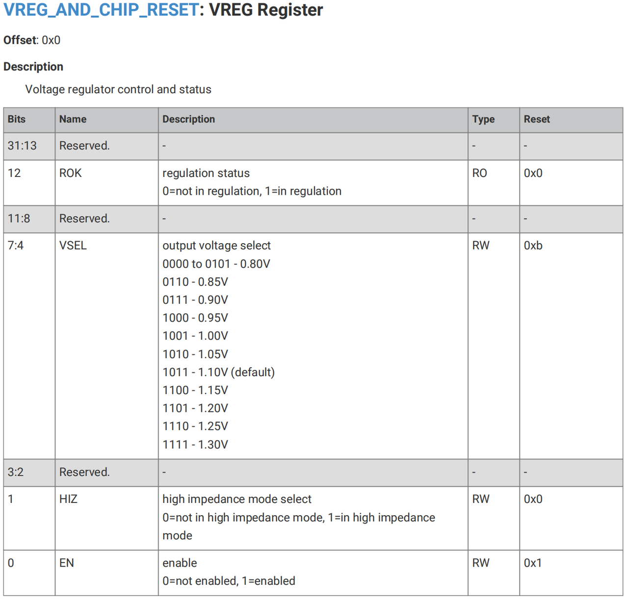
Figure 2.30 RP2040 VREG register bit field description table
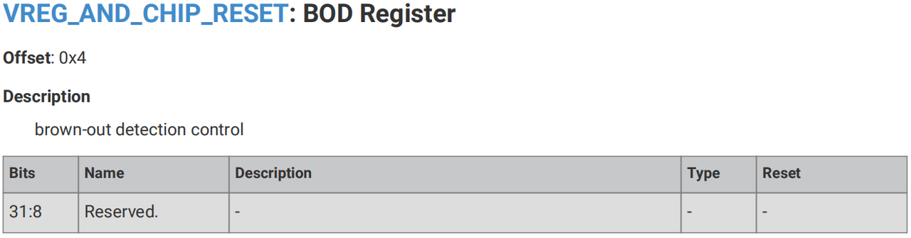
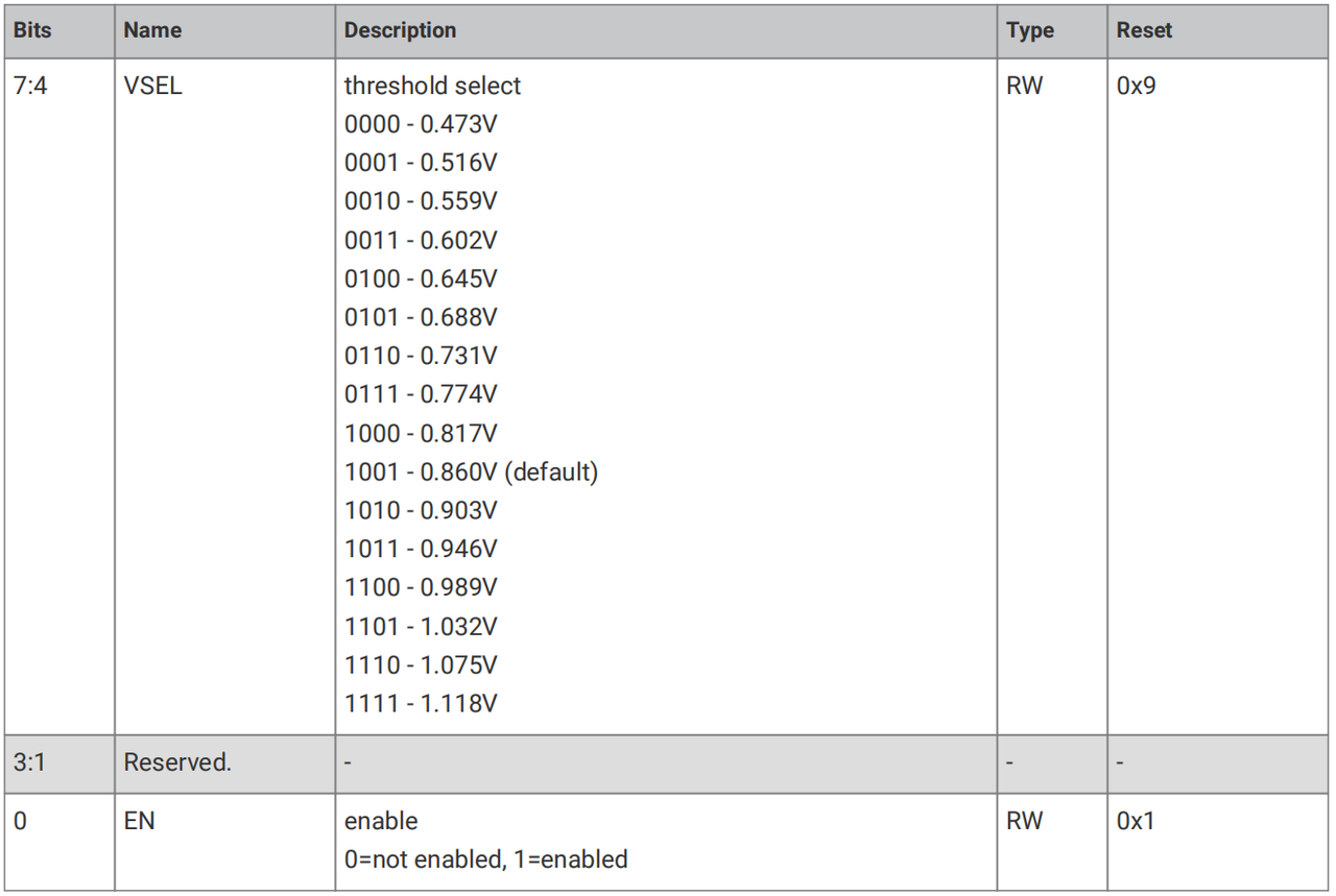
Table 2.31 Description of RP2040 BOD Register Bit Fields
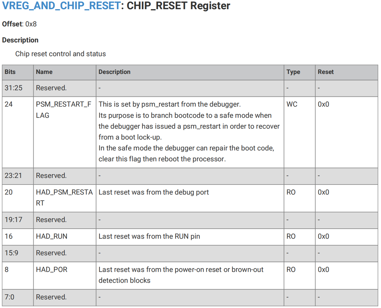
Table 2.32 Description of Bit Fields in RP2040 CHIP_RESET Register
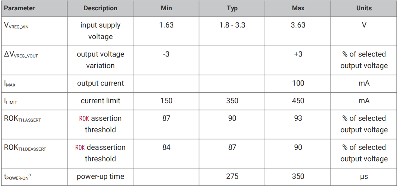
Figure 2.33 RP2040 Power Regulator Parameter Specifications
These values will vary with the load current and capacitance on VREG_VOUT. The above data are the parameter values obtained under the conditions of EN = 1, load current = 0 mA, and VREG_VIN being increased within 100 μs.

