
ZapTrace and the WIZnet W5500: AI-Native PCB Design with First-Class Ethernet Support
ZapTrace and the WIZnet W5500: AI-Native PCB Design with First-Class Ethernet Support
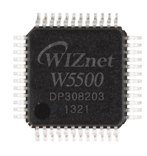
WIZnet - W5500
x 1
The Problem with Electronics Design Tooling
Building a circuit board has always had a software problem. Long before a single component is soldered, engineers spend hours inside EDA tools: drawing schematics, assigning footprints, placing components, routing traces, running design rule checks, and packaging Gerber files for the fab. The hardware insight might arrive in minutes. The toolchain grind that follows takes far longer.
ZapTrace is an open-source project that takes direct aim at this gap. Built by Osman Aslan — a developer whose background spans embedded systems (ESP32, STM32, FreeRTOS), edge ML inference, and agentic AI infrastructure — ZapTrace describes itself as an AI-native, verification-first EDA kernel for agents and engineers. Its pipeline runs from a plain-language design intent all the way to a manufacturing-ready package: intent → normalized design → schematic → ERC → placement → routing → DRC → BOM → Gerber → proof pack.
And the WIZnet W5500 is not just a chip ZapTrace could theoretically support. It is a named, fully-defined, first-class component in ZapTrace's built-in library.
The W5500 in ZapTrace's Component Library
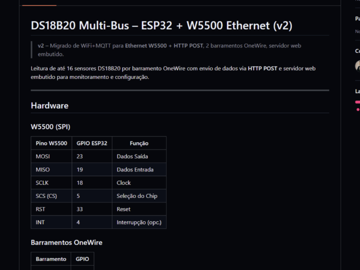
Inside ZapTrace's repository, under data/library/interface/, sits a file called w5500.yaml. It is a complete, structured component definition for the WIZnet W5500 — not a placeholder, not a generic IC template, but a specifically authored entry with the chip's manufacturer, part number, package, datasheet link, lifecycle status, and a full pin map.
The pin map covers every functional group the W5500 exposes:
- Power rails — VDD (3.3 V), GND, VDDPLL, and VDDIO are each defined as
powertype pins, allowing ZapTrace's net classification engine to handle them correctly during copper pour, decoupling capacitor placement, and power integrity checks. - SPI interface — SCLK, MOSI, MISO, and SCS are typed as
inputoroutput, giving the ERC engine the signal direction information it needs to catch misconnected nets before they reach the board. - Control signals — RST (active-low reset) typed as
input, and INT (interrupt output) typed asoutput. - Ethernet differential pairs — TXP/TXN as outputs and RXP/RXN as inputs, allowing the router to recognize and treat these as differential pairs requiring length matching and controlled impedance.
- Crystal pins — XTAL1 and XTAL2 typed as
passive, flagging the 25 MHz oscillator interface for appropriate placement constraints. - PHY mode select — PMODE1, PMODE2, PMODE3 typed as inputs, covering the strapping pins that configure the PHY operating mode.
- LED outputs — LED_LINK and LED_ACT for status indicators.
- Test pin — TEST typed as
inputwith a description noting it should be tied low in normal operation.
Beyond the pin map, the component's properties block captures machine-readable facts about the chip: its interface is spi, its Ethernet speed is 10/100, and tcp_offload is true. That last field is significant — it tells ZapTrace's design engine that this component handles TCP/IP in hardware, which has implications for how the system reasons about the board's networking architecture.
Why Component Library Quality Matters for AI-Driven EDA
In a traditional EDA tool, the component library is a collection of symbols and footprints — visual artifacts that help a human draw a schematic. Correctness is largely the engineer's responsibility: they read the datasheet, they know which pins do what, they set up the connections manually.
In an AI-native system like ZapTrace, the component library is something fundamentally different. It is the structured knowledge base from which the design engine reasons. Every property in the W5500 YAML file is data that ZapTrace's placement engine, router, ERC checker, and net classifier can act on directly.
When ZapTrace sees that TXP and TXN are typed as differential pair outputs, it can apply differential routing rules without being told. When it sees VDDPLL as a power pin separate from VDD, it knows to treat the PLL supply as a noise-sensitive rail requiring dedicated decoupling. When it sees TEST with a description of "tie low," it can flag an unconnected TEST net as an ERC violation. When it sees tcp_offload: true, a sufficiently capable agent working with ZapTrace can understand it is dealing with a hardware-accelerated Ethernet controller rather than a software-stack chip, and reason about the design accordingly.
This is the difference between a library that helps a human draw and a library that helps a machine think.
What ZapTrace Is
ZapTrace ships as four interfaces built on a common core:
A Python SDK for programmatic electronics design — parse a design intent, validate it, place components, route traces, and export manufacturing files entirely from code, without opening a GUI.
A CLI (zaptrace) for rapid iteration at the terminal. A complete design flow from description to Gerber package without leaving the command line.
An MCP server (zaptrace-mcp) exposing 75 agent-facing tools to AI agents via the Model Context Protocol. This is what makes ZapTrace genuinely novel: an AI agent can call into ZapTrace's design tools as structured API calls, treating electronics design as a programmable workflow rather than a GUI to navigate.
A REST API for web-based integration and larger automated pipelines.
Underneath all of these sits a verification engine with Electrical Rule Checking (ERC) and Design Rule Checking (DRC) baked into every stage — not bolted on at the end. Every design run produces a proof pack: a structured, auditable evidence bundle recording what was checked, what rules were applied, and what passed or failed.
A Concrete Design Scenario
Consider what a W5500-based board design looks like inside ZapTrace's workflow, given the library entry above.
An engineer or AI agent describes the intent: a microcontroller board with SPI-to-Ethernet via a W5500, 3.3 V power supply, and USB connectivity. ZapTrace resolves W5500 from its library, instantiates the component with its full pin map, and begins building the netlist.
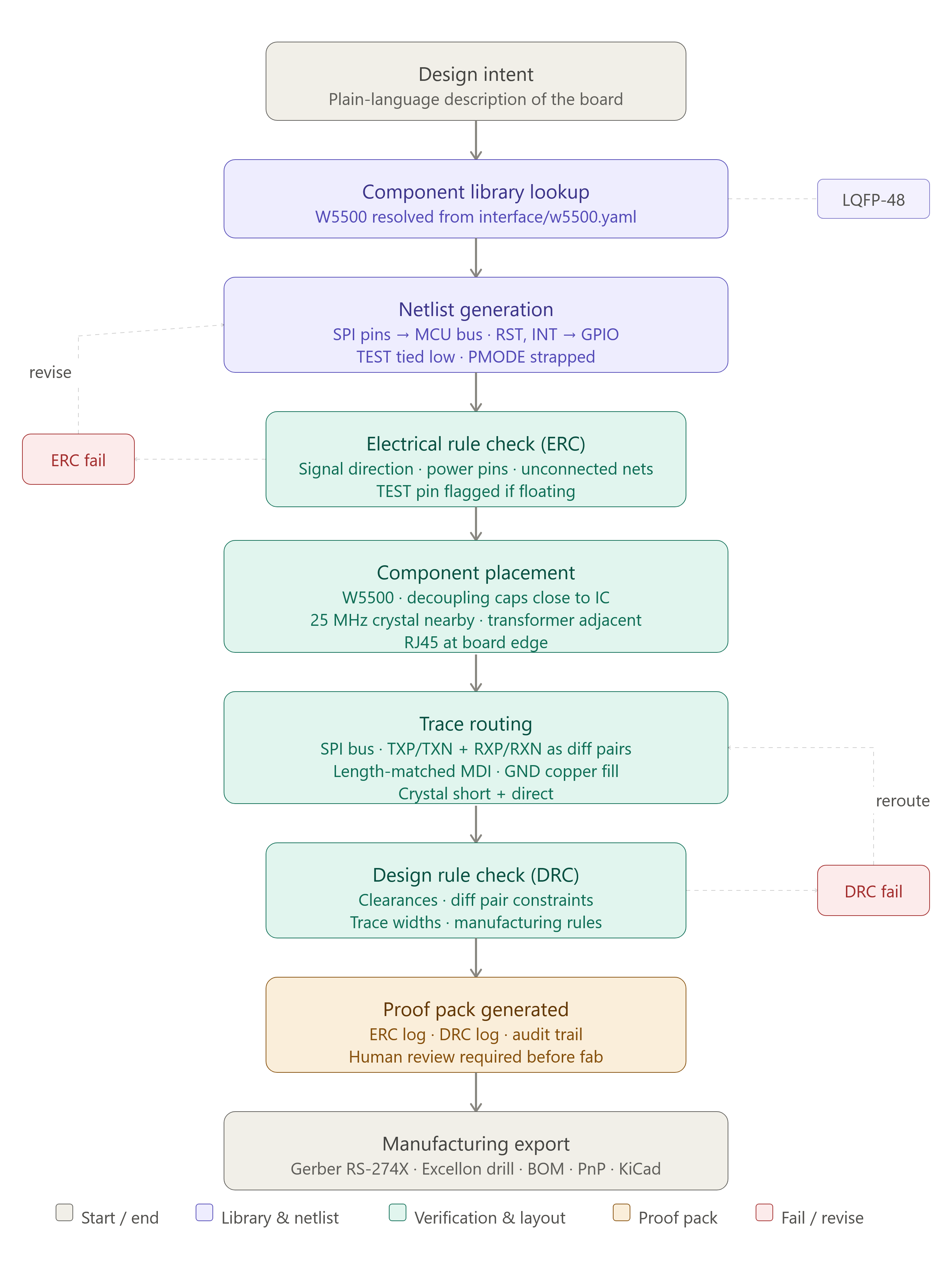
The SPI pins — SCLK, MOSI, MISO, SCS — are classified as high-speed digital signals and connected to the host MCU's SPI bus. The INT pin is routed to an available GPIO for interrupt-driven operation. RST is tied to the MCU's reset logic or a dedicated supervisor circuit. TEST is tied to ground, as the component definition instructs. PMODE pins are strapped for the desired PHY configuration.
On the power side, VDD, VDDPLL, and VDDIO each receive decoupling capacitors placed close to the chip, with GND copper fill applied under the package. The PLL supply gets additional filtering.
XTAL1 and XTAL2 connect to a 25 MHz crystal with its loading capacitors, placed as close to the chip as possible. The crystal nets are flagged for short, direct routing.
TXP/TXN and RXP/RXN route as differential pairs to an Ethernet isolation transformer, with the router enforcing length matching and controlled impedance. From the transformer, the magnetics connect to the RJ45 connector.
When placement and routing complete, ERC runs against the typed pin map — checking signal directions, power connections, unconnected pins, and net integrity. DRC enforces manufacturing rules: clearances, minimum trace widths, differential pair constraints. The proof pack is generated, recording every check and its outcome.
The output: Gerber RS-274X files, Excellon drill, BOM in CSV and JSON, pick-and-place data, and KiCad schematic export — all from a design session that may have been partly or fully agent-driven.
Honest About Its Limits
ZapTrace is pre-1.0. Its schematic synthesis currently works by matching keywords to pre-built templates rather than generating circuits from scratch. Its manufacturing outputs are explicitly experimental, and the project is clear that all outputs require human engineering review before fabrication. The proof pack records what was checked — it does not certify that the board will work.
These are appropriate caveats for software at this stage. The infrastructure is real and running. The W5500 library entry is not aspirational; it is a working component definition that ZapTrace's engine can act on today.
What This Points Toward
ZapTrace's inclusion of the W5500 as a named, fully-typed component in its interface library is more than a convenience feature. It is a signal of where the project is aimed.
The W5500 is one of the more demanding chips to integrate correctly on a custom PCB — differential pair routing, crystal placement constraints, multiple power domains, PHY strapping, and precise decoupling all have to be handled right. Encoding all of that structure into a machine-readable library entry, and building a design engine that can act on it, is the foundational work that makes AI-assisted hardware design something more than autocomplete for schematics.
For WIZnet and the broader community building Ethernet-connected embedded systems, ZapTrace represents an interesting shift in how W5500-based designs could be developed: not by a single engineer working through a GUI, but by programmable, agent-accessible workflows with verification built in from the first net to the final Gerber.
Related Projects
Two projects from the WIZnet Maker community are worth exploring alongside ZapTrace. The KiCad-Happy Test Harness tackles a closely related problem: automating and validating KiCad-based schematic and design workflows. Where ZapTrace approaches EDA automation from a programmatic, agent-first angle, KiCad-Happy works within the KiCad ecosystem directly — the two projects represent complementary philosophies for reducing the manual overhead of electronics design. For anyone building W5500-based boards who already lives in KiCad, it is a natural companion read.
The W5500 Mini Module 3D STEP File is a practical hardware resource relevant to the design scenario described in this article. ZapTrace's W5500 component definition covers the bare IC in its LQFP-48 package, but many real-world designs use a pre-assembled W5500 module — with the magnetics, crystal, and decoupling already integrated — rather than placing the chip directly. The 3D STEP file for this mini module is useful for mechanical clearance checks, enclosure design, and PCB assembly planning when that module form factor is the chosen approach.
ZapTrace is pre-1.0 open-source software. All design outputs require human engineering review before fabrication. This article is based on the project's public repository and component library.