
DIY W5500 Ethernet Module in Altium (2-Layer PCB + 3D Models)
Altium으로 설계한 W5500 Ethernet 모듈 DIY (2-Layer PCB + 3D 모델)
WIZnet - W5500
x 1
Module Ethernet W5500 DIY
Altium Designer로 설계한 2층 구조의 W5500 Ethernet 모듈
프로젝트 소개
임베디드 Ethernet을 구현할 때 많은 개발자들은 완성된 모듈을 바로 사용하는 방식을 선택합니다. 하지만 하드웨어 구조를 직접 이해하고, 필요한 형태로 회로와 PCB를 설계해보고 싶다면 직접 모듈을 만드는 과정 자체가 큰 의미를 가집니다.
Module_Ethernet_W5500_DIY는 W5500 Ethernet 모듈을 직접 설계한 하드웨어 중심 프로젝트입니다. 이 프로젝트는 Altium Designer를 사용해 2층 PCB를 설계했으며, 회로도, 부품 풋프린트, 3D 모델까지 직접 구성한 점이 특징입니다. 단순히 Ethernet 기능을 구현하는 데 그치지 않고, 실제 제작 가능한 형태의 보드 설계 자료를 체계적으로 정리하고 있어, W5500 기반 하드웨어를 설계하려는 개발자에게 좋은 참고가 됩니다.
즉, 이 프로젝트는 단순한 Ethernet 사용 예제가 아니라, W5500 기반 하드웨어 모듈을 직접 설계하고 제작하는 전체 과정을 보여주는 실전형 PCB 설계 레퍼런스라고 볼 수 있습니다.
시스템 구조
이 프로젝트는 W5500 Ethernet 컨트롤러를 중심으로 동작하는 독립형 모듈 설계에 초점을 맞추고 있습니다. 저장소에는 회로 구성이 Resource Schematic, IC Schematic, Peripherals Schematic으로 나뉘어 정리되어 있어, 전원부와 핵심 IC, 주변 회로를 구분해서 살펴볼 수 있습니다.
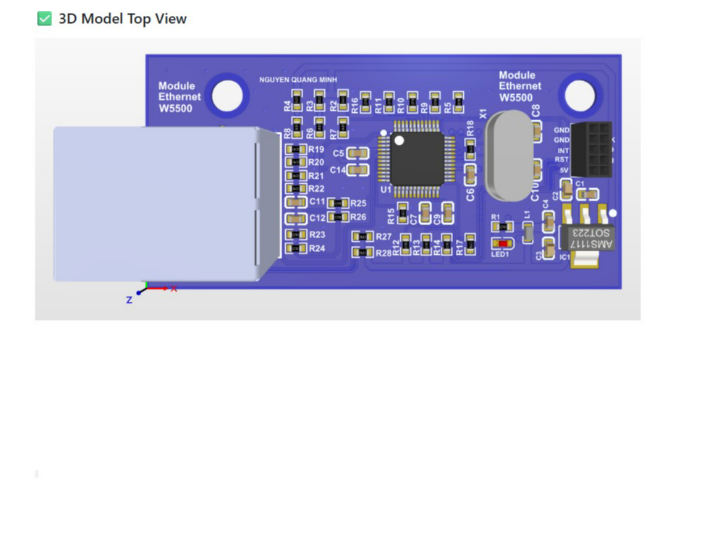
또한 PCB 결과물은 Top Layer, Bottom Layer, Top Overlay, Final Layer로 구분되어 제공되며, 이를 통해 실제 보드 레이아웃이 어떻게 구성되었는지 확인할 수 있습니다. 여기에 더해 3D Model Top View, Bottom View, Multi Board View까지 포함되어 있어, 단순한 회로도 수준을 넘어 완성된 보드 형태를 직관적으로 이해할 수 있습니다.
프로젝트 구조
이 프로젝트의 가장 큰 특징은 제작을 위한 출력 데이터까지 함께 정리되어 있다는 점입니다. 단순히 회로도와 PCB 이미지로 끝나는 것이 아니라, 실제 제조와 조립 단계에 필요한 파일들이 함께 포함되어 있습니다.
주요 산출물은 다음과 같습니다.
- 회로도 이미지 및 PDF
- PCB Top/Bottom Layer 설계 파일
- Gerber 파일
- NC Drill 파일
- BOM
- 3D STEP 파일
- Assembly Drawing
- Pick and Place 파일
이런 구성은 단순한 참고용 프로젝트를 넘어, 실제 생산과 조립까지 염두에 둔 하드웨어 설계 프로젝트라는 점에서 의미가 큽니다. 특히 PCB 제작과 SMT 조립 흐름까지 한 번에 살펴보고 싶은 개발자에게 매우 유용한 자료가 됩니다.
하드웨어 구성
이 프로젝트는 W5500을 중심으로 한 DIY Ethernet 모듈 설계입니다. 저장소 설명에 따르면 모든 부품, 풋프린트, 회로도, 3D 모델이 직접 제작되었으며, 이를 통해 상용 모듈을 단순 복제하는 수준이 아니라 설계 과정을 직접 구축한 사례라는 점이 드러납니다.
또한 2층 PCB 구조로 설계되었다는 점은 실제 제작 난이도와 비용 사이에서 현실적인 균형을 고려한 선택으로 볼 수 있습니다. 복잡한 다층 보드 대신 2층 보드로 W5500 모듈을 구현했다는 점은, 개인 제작이나 소규모 양산 관점에서도 참고 가치가 있습니다.
핵심 기능
이 프로젝트의 핵심은 기능 데모보다 설계 완성도와 제작 가능성에 있습니다.
첫째, W5500 기반 Ethernet 모듈을 독립적으로 설계했다는 점이 중요합니다.
둘째, 회로도부터 PCB 레이아웃, 3D 모델까지 전체 하드웨어 설계 과정을 포함하고 있습니다.
셋째, Gerber, BOM, Drill, Pick and Place 파일까지 제공해 실제 제조 단계로 이어질 수 있는 형태를 갖추고 있습니다.
즉, 이 프로젝트는 단순한 개발 보드 활용 예제가 아니라, Ethernet 모듈을 직접 설계하고 제작하는 흐름 전체를 보여주는 하드웨어 설계 프로젝트입니다.
W5500의 강점
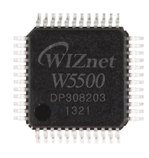
이 프로젝트에서 W5500은 핵심 Ethernet 컨트롤러 역할을 담당합니다. W5500은 MCU와 SPI로 연결할 수 있고, 안정적인 유선 Ethernet 인터페이스를 제공하기 때문에 다양한 임베디드 시스템에서 활용도가 높습니다.
하드웨어 설계 관점에서 보면 W5500은 이미 검증된 Ethernet 칩이기 때문에, 커스텀 보드 설계 시 비교적 명확한 구조를 바탕으로 회로를 구성할 수 있다는 장점이 있습니다. 이 프로젝트는 그런 장점을 바탕으로, 상용 모듈에 의존하지 않고 직접 설계한 W5500 Ethernet 모듈을 구현했다는 점에서 의미가 큽니다.
이런 구조는 다음과 같은 방향으로 확장하기 좋습니다.
- 맞춤형 Ethernet 확장 보드 제작
- 산업용 제어 장비용 커스텀 네트워크 모듈
- 교육용 PCB 설계 실습 자료
- 소규모 양산을 위한 Ethernet 하드웨어 레퍼런스
빌드와 적용
이 프로젝트는 소프트웨어 예제보다는 하드웨어 제작과 설계 자료 제공에 초점이 맞춰져 있습니다. 저장소에는 실제 PCB 제조와 조립에 활용할 수 있는 출력 파일이 포함되어 있어, 단순히 아이디어를 보여주는 수준을 넘어 바로 제작 단계로 이어질 수 있는 구성을 갖추고 있습니다.
따라서 이 프로젝트는 W5500 기반 모듈을 직접 만들고 싶은 개발자나, Ethernet 하드웨어 설계를 학습하려는 사용자에게 실질적인 참고 자료가 될 수 있습니다.
마무리
Module_Ethernet_W5500_DIY는 단순히 W5500을 사용하는 프로젝트가 아닙니다.
이 프로젝트는 회로 설계, PCB 레이아웃, 3D 모델링, 제조용 출력 데이터까지 포함해, W5500 기반 Ethernet 모듈을 직접 설계하는 과정을 전체적으로 보여줍니다.
완성된 모듈을 사용하는 단계에서 더 나아가, Ethernet 하드웨어 자체를 설계하고 구현해보고 싶다면 이 프로젝트는 매우 좋은 참고 사례가 될 것입니다.
FAQ
Q1. 이 프로젝트의 핵심은 소프트웨어인가요, 하드웨어인가요?
이 프로젝트는 소프트웨어 예제보다 하드웨어 설계와 PCB 제작에 더 초점을 맞추고 있습니다.
Q2. 어떤 설계 툴로 제작되었나요?
Altium Designer를 사용해 2층 PCB로 설계되었습니다.
Q3. 어떤 자료가 포함되어 있나요?
회로도, PCB 레이아웃, 3D 모델, Gerber, BOM, Drill, Assembly, Pick and Place 파일 등이 포함되어 있습니다.
Q4. 이 프로젝트는 어떤 사람에게 유용한가요?
W5500 기반 Ethernet 모듈을 직접 설계하거나, PCB 제작 흐름까지 포함한 하드웨어 프로젝트를 참고하려는 개발자에게 유용합니다.
Module Ethernet W5500 DIY
A Two-Layer W5500 Ethernet Module Designed in Altium Designer
Project Introduction
When implementing Ethernet in embedded systems, many developers choose to use ready-made modules. That approach is practical, but designing the hardware directly provides a much deeper understanding of how the Ethernet interface is built and integrated.
Module_Ethernet_W5500_DIY is a hardware-focused project that builds a custom W5500 Ethernet module from the ground up. The project uses Altium Designer to create a two-layer PCB, and includes custom-created schematics, component footprints, and 3D models. Rather than simply demonstrating Ethernet functionality, it presents a complete set of design resources for a manufacturable W5500-based hardware module.
In that sense, this is not just an Ethernet usage example. It is a practical PCB design reference that shows the full process of designing and preparing a custom W5500 Ethernet module for production.
System Architecture
The project is centered around a standalone hardware module based on the W5500 Ethernet controller. The repository organizes the circuit design into sections such as Resource Schematic, IC Schematic, and Peripherals Schematic, making it easier to understand the power stage, core IC section, and peripheral circuitry separately.
The PCB results are also presented in multiple views, including Top Layer, Bottom Layer, Top Overlay, and Final Layer. In addition, the repository provides 3D model views from the top, bottom, and multi-board perspectives, which helps visualize the completed board beyond the schematic and layout level.
Project Structure
One of the strongest aspects of this project is that it includes not only design visuals, but also the full set of files needed for production. It goes beyond basic schematic sharing and provides materials that support actual PCB fabrication and assembly.
The main outputs include:
- schematic images and PDF files
- top and bottom PCB layout data
- Gerber files
- NC Drill files
- BOM
- 3D STEP file
- assembly drawings
- pick and place files
This makes the project more than a concept design. It is a hardware development project prepared with real manufacturing and assembly in mind, which is especially useful for developers who want to study the full flow from PCB design to production.
Hardware Setup
This project is a DIY Ethernet module built around the W5500. According to the repository, all components, footprints, schematics, and 3D models were created directly as part of the project. That makes it more than just a reuse of an existing commercial module design.
The use of a two-layer PCB structure is also notable. It reflects a practical balance between hardware complexity, cost, and manufacturability. Instead of relying on a more complex multilayer design, the project demonstrates how a W5500-based Ethernet module can be implemented on a realistic two-layer board.
Key Features
The core value of this project lies in design completeness and manufacturability rather than in a firmware demonstration.
First, it presents a fully custom W5500-based Ethernet module design.
Second, it includes the entire hardware design flow from schematic to PCB layout and 3D modeling.
Third, it provides manufacturing-ready outputs such as Gerber, BOM, Drill, and Pick and Place files, making it possible to move directly toward fabrication.
This makes the project a complete hardware design reference for building a custom Ethernet module, not just a simple development board example.
Strength of W5500
In this project, the W5500 serves as the core Ethernet controller. Since it can be connected to a microcontroller over SPI and provides a stable wired Ethernet interface, it is widely used in embedded systems.
From a hardware design perspective, W5500 is also a strong choice because it is already well established and suitable for custom board development. This project highlights that strength by showing how a fully custom Ethernet module can be built around it without relying entirely on off-the-shelf modules.
This kind of design can be extended toward applications such as:
- custom Ethernet expansion boards
- industrial control network modules
- educational PCB design references
- small-scale production hardware for wired networking
Build and Usage
This project is focused more on hardware design and manufacturing preparation than on firmware development. Since the repository includes production-related output files, it offers more than a design concept and can serve as a direct starting point for PCB fabrication and assembly.
For developers who want to build their own W5500-based module, or for those studying the full process of Ethernet hardware design, this project provides a very practical reference.
Conclusion
Module_Ethernet_W5500_DIY is more than a simple project using the W5500.
It brings together schematic design, PCB layout, 3D modeling, and manufacturing output files into one complete example of a custom W5500 Ethernet module.
For anyone who wants to move beyond using ready-made modules and start designing Ethernet hardware directly, this project is a strong and valuable reference.
FAQ
Q1. Is this project mainly about software or hardware?
This project is primarily focused on hardware design and PCB development rather than firmware.
Q2. Which design tool was used?
It was designed as a two-layer PCB using Altium Designer.
Q3. What resources are included?
The repository includes schematics, PCB layouts, 3D models, Gerber files, BOM, drill files, assembly drawings, and pick and place files.
Q4. Who is this project useful for?
It is useful for developers who want to design their own W5500-based Ethernet module or learn the full workflow of PCB-based Ethernet hardware development.