What is 12 0x20000000? The Memory Management Logic Behind the RP2040 Address Map
This article explains RP2040's bus architecture and address mapping that govern internal data transmission and resource access.
COMPONENTS
PROJECT DESCRIPTION
Introduction to System Features and Structure
1. Bus Interconnection Architecture
The bus interconnection structure is the "data transportation system" inside a chip — it governs how data and instructions are transmitted between various functional modules (cores, memory, peripherals), making it one of the core architectures that impact a chip's operating efficiency. Understanding this structure allows one to clearly grasp how the chip avoids data transmission congestion and the communication priorities of different modules, which is the key to understanding the chip's performance bottlenecks and resource scheduling logic.
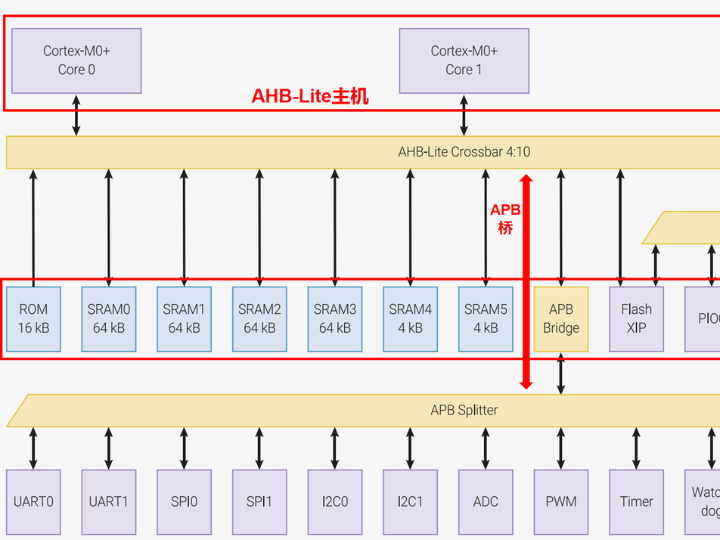
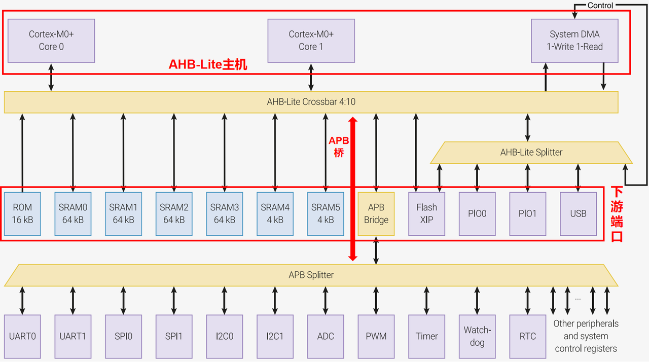
Figure 2.9 Block Diagram of Bus Interconnection Structure of RP2040 Chip
This diagram illustrates the "internal communication network" of the RP2040, with the core logic as follows:
AHB-Lite Master (Upstream Port): It serves as the initiator of data requests, corresponding to four traffic initiators: two processor cores (Core0 and Core1), the read port of DMA, and the write port of DMA, which are responsible for sending read/write data requests to other modules.
AHB-Lite Crossbar (bus hub): It acts as a "traffic control center", which distributes the requests from 4 master devices to 10 "downstream ports"(i. e. the modules to which the data is to be delivered); it can complete up to 4 transmissions of 32-bit data per clock cycle, ensuring the efficiency of data interaction.
Downstream port (destination module): refers to the recipient of a data request, which falls into three categories:
Storage Class Module: Consists of ROM, Flash XIP, and the partitioned SRAM0~5 (each SRAM occupies an independent port). Splitting the SRAM into multiple ports is designed to enable "parallel access by multiple modules" — for example, when Core0 is accessing SRAM0, the DMA can access SRAM1 simultaneously — so as to avoid access congestion of storage resources.
High-speed peripheral modules: including "Fast AHB-Lite peripherals" such as PIO0, PIO1 and USB, which are directly connected to the bus hub to adapt to the requirements of high-speed data transmission.
Low-speed peripheral modules: These include peripherals such as UART, SPI, and I2C, which are connected to the bus hub via the "APB bridge" — the APB bridge acts as a "slow lane adapter", ensuring that communications from low-speed peripherals do not compromise the transmission efficiency of high-speed modules.
2. Address Mapping
To understand address mapping, we first need to clarify its core definition: Address mapping refers to the rules by which a chip assigns a unique "digital address" to all its internal resources (including ROM, SRAM, peripheral registers, etc.)— it is equivalent to assigning a "house number" to every storage block and functional module inside the chip; modules such as the core and DMA can accurately locate and access the corresponding resource through this "house number"(address).
The reason why address mapping is required is that the arithmetic/control modules of the chip (such as dual-core processors and DMA) can only locate resources by means of "addresses": for example, when the kernel needs to read data from SRAM or configure the communication parameters of a UART, it must first find the storage area of the SRAM and the control registers of the UART through the corresponding addresses — without address mapping, these modules are just like "rooms without house numbers" that cannot be located or accessed at all. The essence of address mapping is to establish a unique accessible identifier for resources, which serves as the fundamental rule for internal communication within the chip.
Address mapping works in close coordination with the aforementioned "SRAM partitioning" — take the SRAM of the RP2040 as an example: As mentioned earlier, the SRAM is physically divided into 6 banks (SRAM0 to SRAM5), which is designed to support "parallel access" by multiple modules (for instance, while Core0 is accessing SRAM0, the DMA can access SRAM1 simultaneously);The address mapping table assigns independent address ranges to these 6 banks (for example, SRAM0_BASE is 0x21000000 and SRAM1_BASE is 0x21010000).
In this way, when Core0 accesses addresses starting with 0x21000000, it actually corresponds to the physical SRAM0; when DMA accesses addresses starting with 0x21010000, it corresponds to the physical SRAM1 —— address mapping enables different modules to access "different physical partitions" via "different house numbers", which not only realizes precise resource positioning, but also achieves "parallel access" in coordination with the physical partitions of SRAM, avoiding resource conflicts between modules and improving data access efficiency.
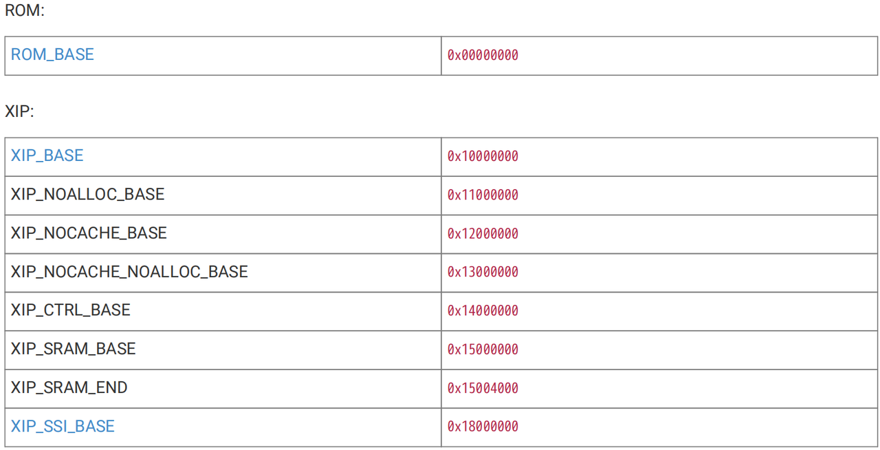
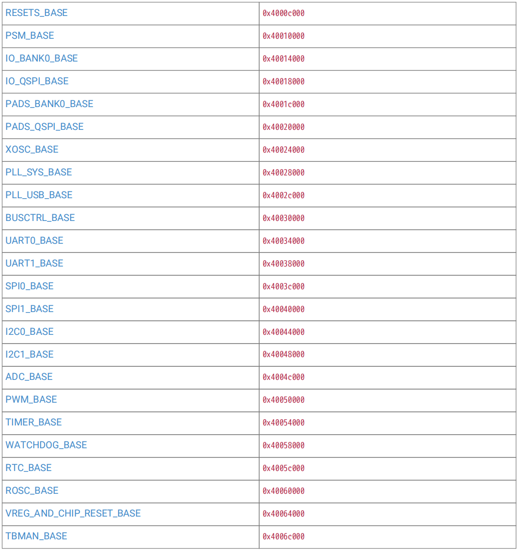
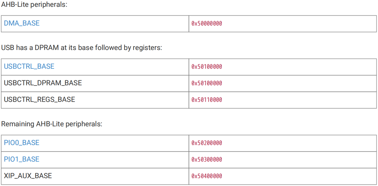
The address mapping of RP2040 is as follows:
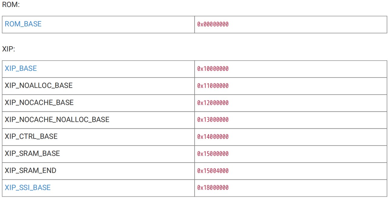
Figure 2.10 RP2040 Chip Address Map (Full Series)
As can also be seen from the address mapping table in the figure:
Different types of resources are allocated to distinct address ranges (for example, ROM starts at 0x00000000, SRAM starts at 0x20000000, and peripherals start at 0x40000000), which makes it easier for modules to distinguish whether the target to be accessed is a memory or a peripheral;
Different sub-modules of the same type of resource (e. g. SRAM0 to SRAM5) have consecutive yet independent address ranges, which not only ensures the integrity of the storage but also supports partitioned access.