



W5500 Deep Dive: Hardware TCP/IP Stack, SPI & Register Mapping Explained
It analyzes W5500 hardware TCP/IP stack, SPI interface communication mechanism and complete register‑memory mapping workflow.
Introduction to W5500 Ethernet Module
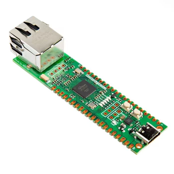
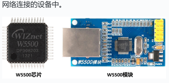
W5500 is a chip produced by WIZnet. It integrates TCP/IP protocol stack together with 10/100 MAC and PHY. This single‑chip solution implements network connectivity and fits embedded‑system network applications perfectly. The W5500 communicates with the host MCU via SPI. It features simple interface and fast transfer speed. Users can conveniently write driver code to control the W5500 for data receiving and transmitting. In real‑world deployment, W5500 can be used in smart‑home devices, IoT gateways and other network‑connected equipment.
Main features of the W5500 chip:
Hard‑wired TCP/IP protocols supported: TCP, UDP, ICMP, IPv4, ARP, IGMP, PPPoE Supports up to 8 independent sockets simultaneously; 32 KB internal memory for transmit / receive buffers Power‑down mode supported; remote Wake‑on‑LAN function over UDP High‑speed SPI interface (SPI Mode 0 and Mode 3); data rate up to 133 Mbps Built‑in 10BaseT / 100BaseTX Ethernet PHY Auto‑negotiation support (full‑duplex / half‑duplex, 10 Mbps / 100 Mbps); IP fragmentation is not supported 3.3 V operating voltage with 5 V‑tolerant I/O signals; 48‑pin lead‑free LQFP package (7×7 mm, 0.5 mm pitch) LED output pins (full‑duplex/half‑duplex, link, speed, activity)
- Internal Architecture of W5500 Chip
The block diagram of W5500 internal structure is shown below:
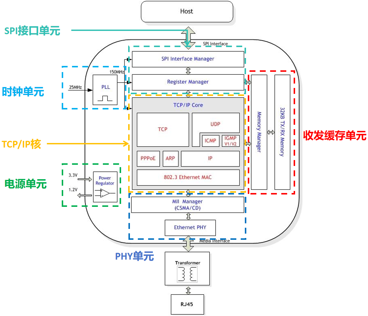
Its internal modules are described as follows:
Clock Unit Requires a 25 MHz clock source. An internal PLL multiplies the clock up to 150 MHz.
Power Unit Powered by 3.3 V and generates an internal 1.2 V power supply.
PHY Unit Integrated physical‑layer PHY for signal conversion and transmission. Supports auto‑link detection and cable‑type detection. Implements IEEE 802.3 Ethernet MAC. Supports 10/100 Mbps auto‑negotiation. The MII Manager controls the PHY for link‑layer network communication.
TCP/IP Core Complete built‑in TCP/IP stack supporting TCP, UDP, IP, ARP, ICMP, IGMP and other protocols. Provides socket‑oriented interfaces for up to 8 sockets. Developers only need to implement UDP and TCP communication through socket programming.
Transmit‑Receive Buffer Unit Contains transmit buffer and receive buffer for packet storage. Users may configure register settings of W5500 to assign appropriate buffer size for each socket.
SPI Interface Unit Communication port for host‑controller connection. Supports maximum 80 MHz clock frequency. Host accesses W5500 registers through SPI to complete configuration and network‑communication tasks.
- W5500 Pins and Peripheral Circuits
Pin assignment of W5500 chip:
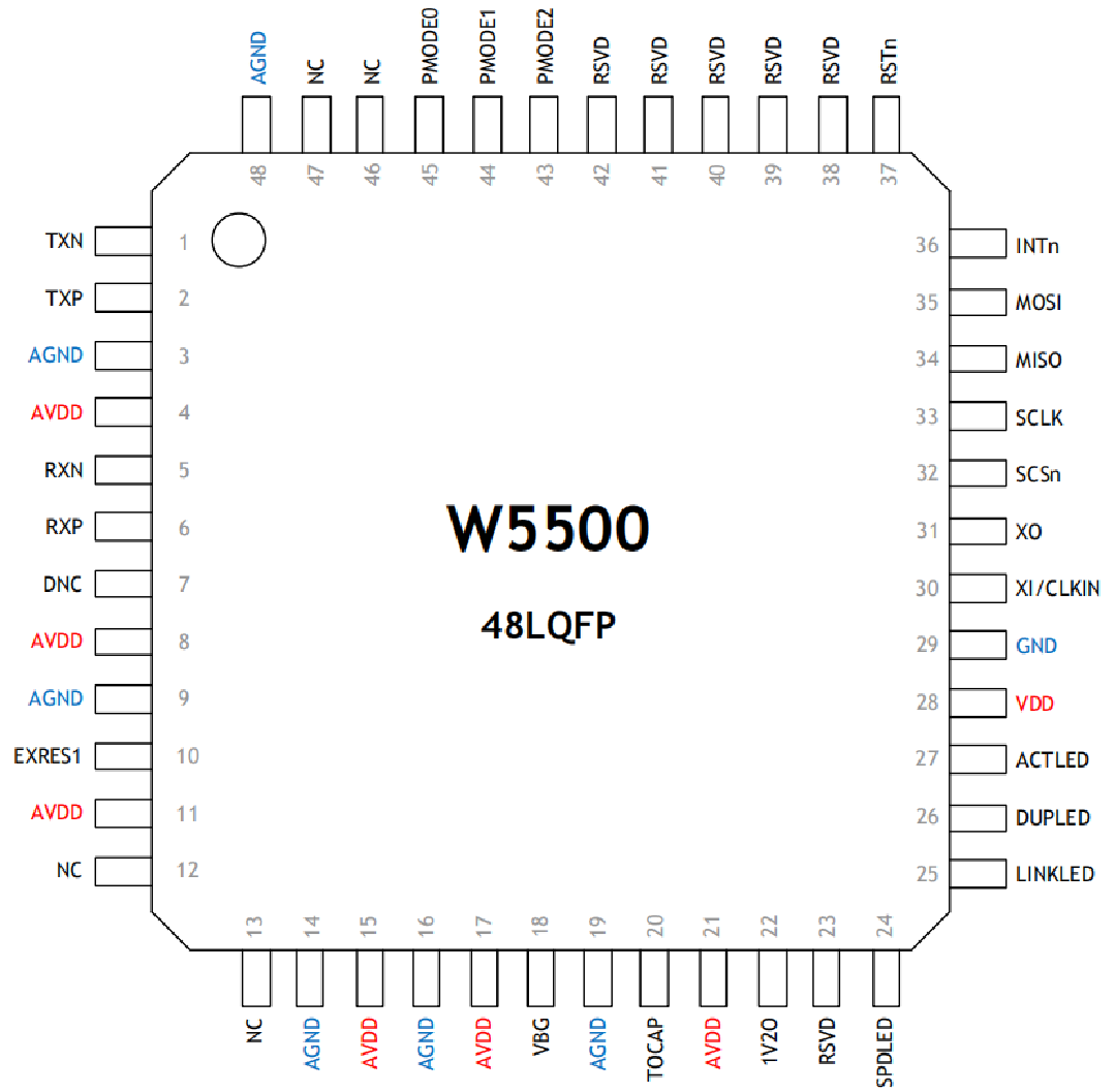
Pin functions are listed below:
Brief pin grouping:
Power and Ground
VCC (3.3 V) 3.3 V power supply input.
GND Digital ground pin.
AVDD Analog 3.3 V power supply.
AGND Analog ground pin.
Network Interface Pins
TXN (1) Differential transmit negative signal.
TXP (2) Differential transmit positive signal.
RXN (5) Differential receive negative signal.
RXP (6) Differential receive positive signal.
Reset and Clock
RSTn (37) Reset signal, active‑low.
XI/CLKIN (30) External 25 MHz crystal‑oscillator input or external clock input.
XO (31) External 25 MHz crystal‑oscillator output.
SPI Interface Pins
SCSn (32) SPI chip‑select signal, active‑low.
SCLK (33) SPI serial clock signal.
MOSI (35) SPI master‑out slave‑in signal.
MISO (34) SPI master‑in slave‑out signal.
INTn (36) Interrupt output signal, active‑low.
Indicator LED Pins
SPDLED (24) Speed indicator. Low level = 100 Mbps; high level = 10 Mbps.
LINKLED (25) Link indicator. Low level = link established; high level = no link.
DUPLED (26) Full‑duplex / half‑duplex indicator. Low level = full‑duplex; high level = half‑duplex.
ACTLED (27) Activity indicator. Low level = carrier‑sense detected; high level = no carrier‑sense.
Miscellaneous Pins
EXRES1 (10) External reference‑resistor pin. Connect a 12.4 kΩ resistor for internal analog‑circuit biasing.
TOCAP (20) External reference‑capacitor pin. Connect a 4.7 µF capacitor.
1V2O (22) 1.2 V regulated‑voltage output. Connect a 10 nF capacitor.
PMODE2 (43), PMODE1 (44), PMODE0 (45) PHY operation‑mode selection pins.
VBG (18) Band‑gap voltage output; leave floating.
RSVD (23, 38, 39, 40, 41, 42) Reserved pins; tie to ground.
Reference peripheral‑circuit schematic:
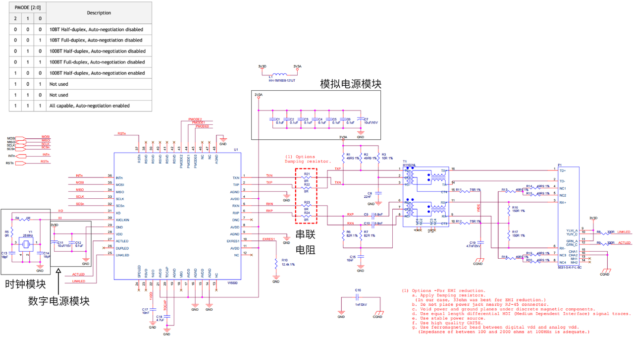
The network interface connects to RJ45 jack through a LAN transformer. The transformer provides electrical isolation and impedance matching. Damping resistors are placed in series on network lines to suppress circuit oscillation.
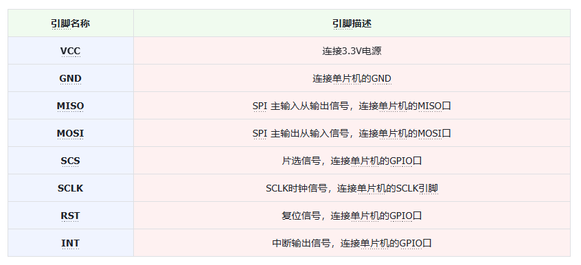
When using W5500, the MCU shall connect the following pins of the chip:
- Host Interface and SPI Frame Format
W5500 works as SPI slave device to communicate with host. Four signal lines are required: SCSn, SCLK, MOSI, MISO.
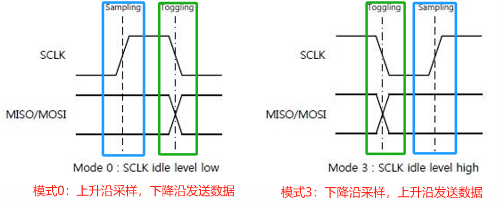
There are four SPI modes defined by clock polarity and phase. Mode 0 (CPOL = 0, CPHA = 0) and Mode 3 (CPOL = 1, CPHA = 1) sample data on rising clock edge and prepare data on falling clock edge. W5500 only supports these two modes. All bytes are transmitted MSB‑first.
W5500 supports both fixed‑length and variable‑length SPI transactions, selected by OM bits inside SPI‑frame control field.
When OM[1:0] = '01' / '10' / '11' : FDM Fixed‑Data‑Length Mode
Data is transferred in fixed‑size blocks. Used for scenarios with known constant data length such as real‑time control. SCSn may be permanently tied low. The host SPI port is exclusively occupied by W5500 and cannot be shared with other SPI slaves.
When OM[1:0] = '00' : VDM Variable‑Data‑Length Mode
Transaction length can change dynamically for applications with uncertain payload size. SCSn acts as transaction‑boundary marker and must be controlled by host. SCSn falling‑edge (high‑to‑low): start of one SPI frame. SCSn rising‑edge (low‑to‑high): end of one SPI frame.
W5500 SPI frame consists of 16‑bit Address Phase, 8‑bit Control Phase and N‑byte Data Phase.
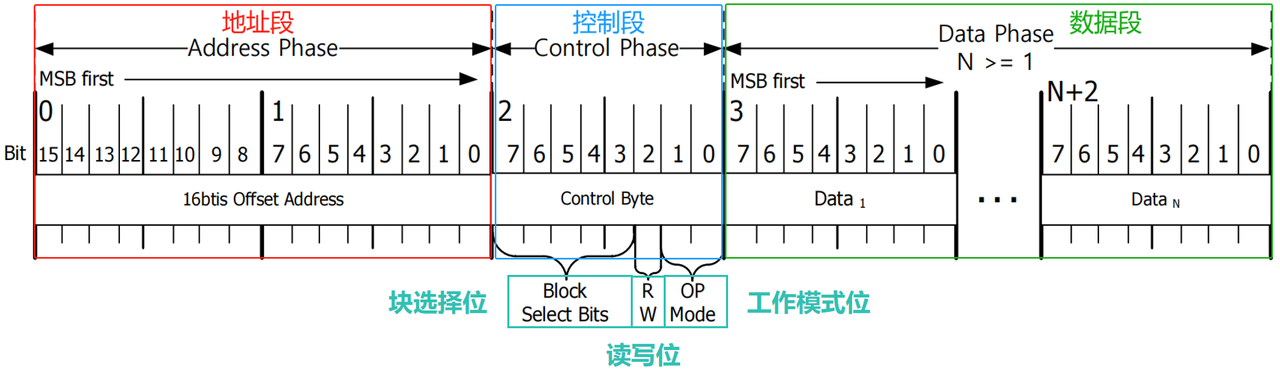
Address Phase 16‑bit offset address for read/write operations. W5500 uses auto‑address‑increment to implement burst sequential access.
Control Phase Contains three sub‑fields: Operation‑Mode (OM), Read‑Write‑Bit (RWB), Block‑Select‑Bits (BSB).
OM Operation Mode, lowest two bits of control byte, selects transaction‑length mode. 00b: Variable‑length mode 01b: Fixed length, 1‑byte data phase 10b: Fixed length, 2‑byte data phase 11b: Fixed length, 4‑byte data phase In VDM mode: host pulls SCSn low to start transaction; after N‑byte data transfer host pulls SCSn high to terminate transaction. In FDM mode: OM determines data‑phase byte count; W5500 terminates transaction automatically once specified bytes have been shifted out/in. SCSn must stay low for the whole transaction regardless of mode.
RWB Read / Write Bit 0 = write operation 1 = read operation
BSB Block Select Bits Selects target internal register block or memory space inside W5500. There is one General Register Block for configuring local‑IP, MAC‑address, subnet‑mask, gateway and PHY parameters. Eight Socket Register Blocks for socket‑level TCP/UDP programming. Each socket owns independent transmit‑buffer and receive‑buffer for network traffic.
Data Phase Actual payload bytes. Length is determined by OM bits and SCSn signal. Transfer direction is controlled by RWB bit.
- Register and Memory Organization
4.1 Overview of W5500 Register and Memory Layout
W5500 includes one General Register Block, eight Socket Register Blocks and per‑socket TX/RX buffer blocks.
Each socket TX buffer resides inside the physical 16 KB TX memory; default allocation per socket is 2 KB. Valid address range for TX buffer: 0x0000 ~ 0xFFFF (16‑bit offset). Each socket RX buffer resides inside the physical 16 KB RX memory; default allocation per socket is 2 KB. Valid address range for RX buffer: 0x0000 ~ 0xFFFF (16‑bit offset).
Blocks are selected by BSB[4:0] inside SPI frame:
| BSB [4:0] | Meaning |
|---|---|
| 00000 | Select General Registers |
| 00001 | Select Socket 0 Registers |
| 00010 | Select Socket 0 TX Buffer |
| 00011 | Select Socket 0 RX Buffer |
| 00100 | Reserved |
| 00101 | Select Socket 1 Registers |
| 00110 | Select Socket 1 TX Buffer |
| 00111 | Select Socket 1 RX Buffer |
| 01000 | Reserved |
| 01001 | Select Socket 2 Registers |
| 01010 | Select Socket 2 TX Buffer |
| 01011 | Select Socket 2 RX Buffer |
| 01100 | Reserved |
| 01101 | Select Socket 3 Registers |
| 01110 | Select Socket 3 TX Buffer |
| 01111 | Select Socket 3 RX Buffer |
| 10000 | Reserved |
| 10001 | Select Socket 4 Registers |
| 10010 | Select Socket 4 TX Buffer |
| 10011 | Select Socket 4 RX Buffer |
| 10100 | Reserved |
| 10101 | Select Socket 5 Registers |
| 10110 | Select Socket 5 TX Buffer |
| 10111 | Select Socket 5 RX Buffer |
| 11000 | Reserved |
| 11001 | Select Socket 6 Registers |
| 11010 | Select Socket 6 TX Buffer |
| 11011 | Select Socket 6 RX Buffer |
| 11100 | Reserved |
| 11101 | Select Socket 7 Registers |
| 11110 | Select Socket 7 TX Buffer |
| 11111 | Select Socket 7 RX Buffer |
4.2 General Register Block
General‑register block configures W5500 local‑IP address, MAC address, subnet mask, gateway and PHY settings.
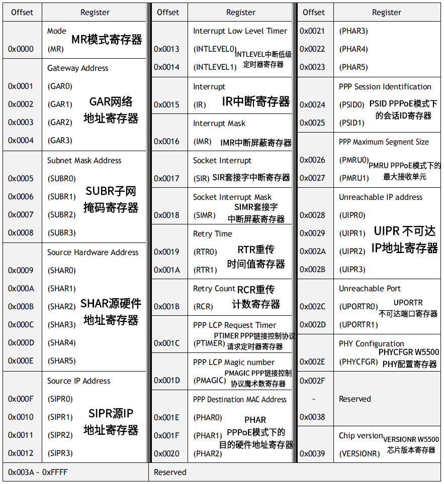
Register descriptions:
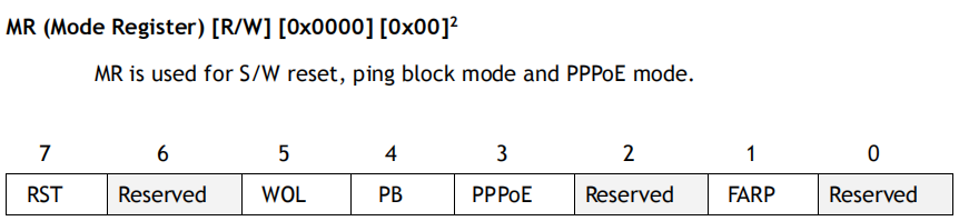
MR Mode Register Used for software reset, ping‑block mode and PPPoE‑mode configuration.
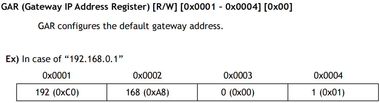
GAR Gateway Address Register Configure gateway IP‑address.
SUBR Subnet‑Mask Register Configure subnet‑mask value.
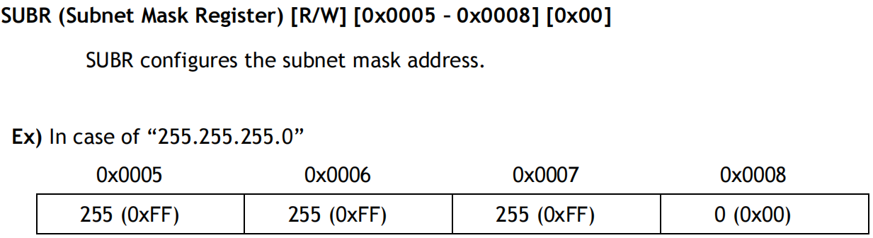
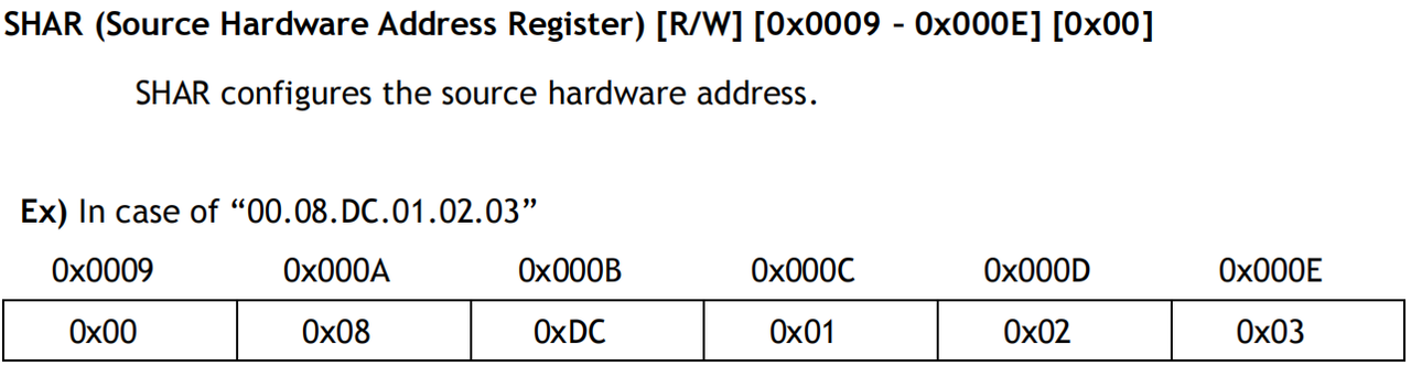
SHAR Source Hardware‑Address Register Configure device MAC‑address.
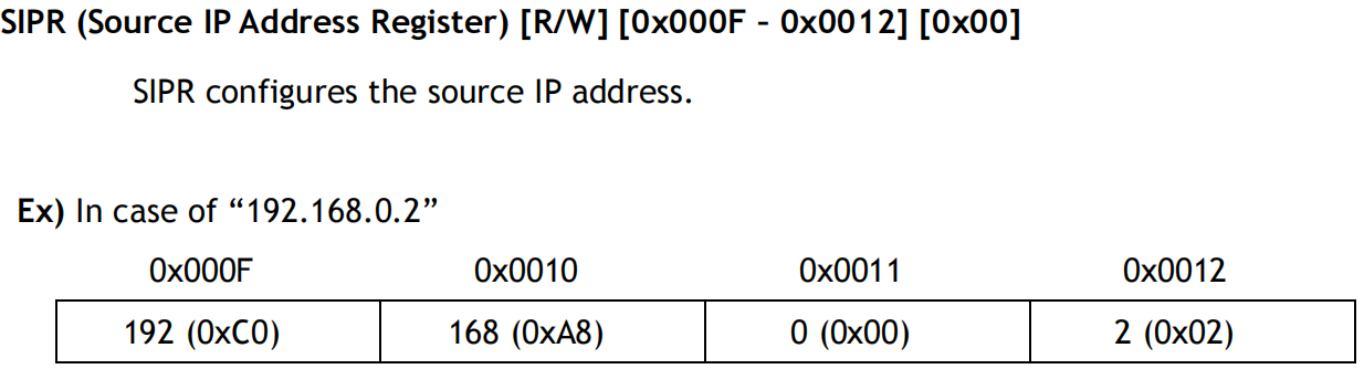
SIPR Source IP‑Address Register Configure device IP‑address.
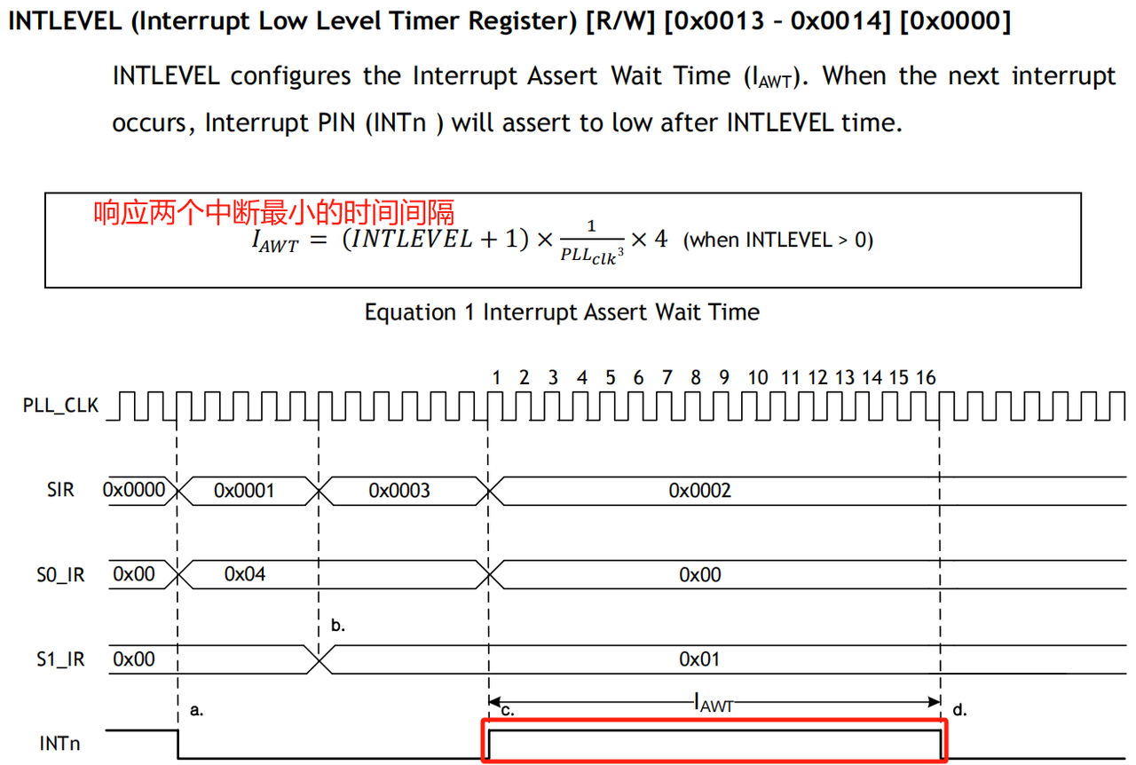
INTLEVEL Interrupt Low‑Level Timer Register Set interrupt low‑level timer value.
IR Interrupt Register Shows current interrupt status flags.
IMR Interrupt Mask Register Configure interrupt masking bits.
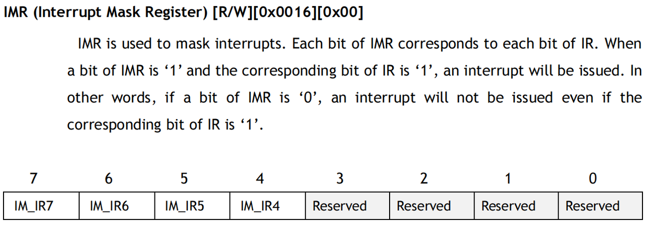
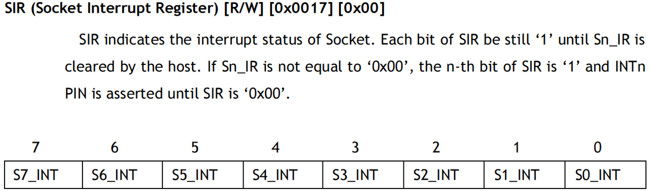
SIR Socket Interrupt Register Shows per‑socket interrupt status.
SIMR Socket Interrupt Mask Register Configure per‑socket interrupt‑mask bits.
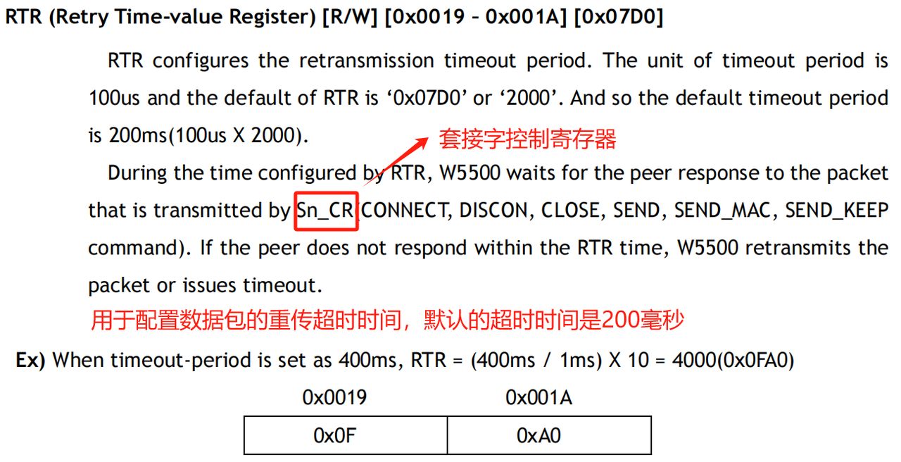
RTR Retry Time Register Set TCP retransmission timeout value.
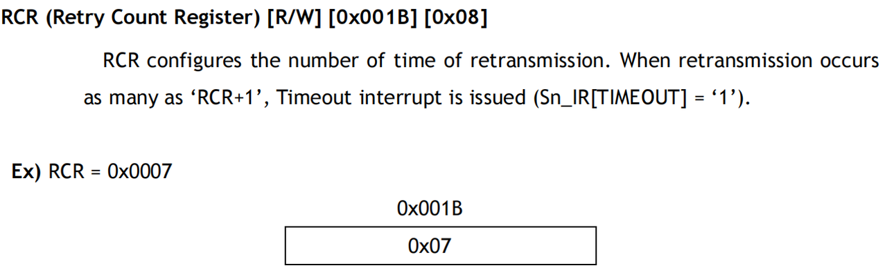
RCR Retry Count Register Set maximum TCP retransmission‑attempt count.
PTIMER PPP LCP Request Timer Register Timer setting for PPP LCP echo‑request transmission.
PMAGIC PPP LCP Magic‑Number Register Magic‑number value used in PPP LCP echo‑requests.
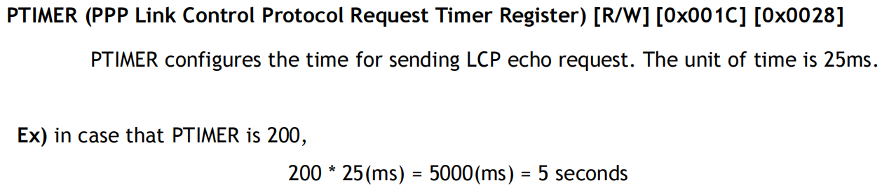
PHAR PPPoE Destination Hardware‑Address Register Store MAC‑address of PPPoE server under PPPoE mode.
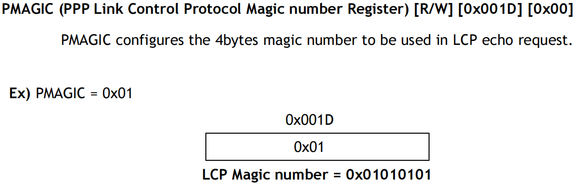
PSID PPPoE Session‑ID Register Store PPPoE session‑ID.
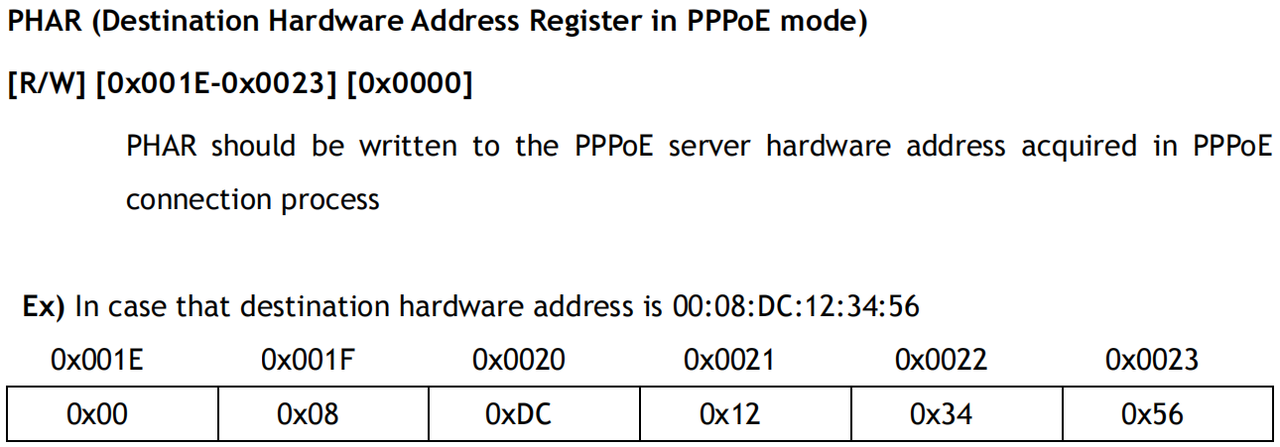
PMRU PPPoE Maximum Receive Unit Register Set PPPoE MRU value.
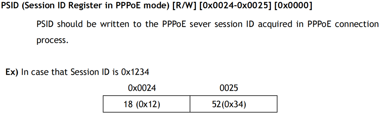
UIPR Unreachable IP‑Address Register Record IP‑address of last unreachable destination.
UPORTR Unreachable Port Register Record port number of last unreachable destination.
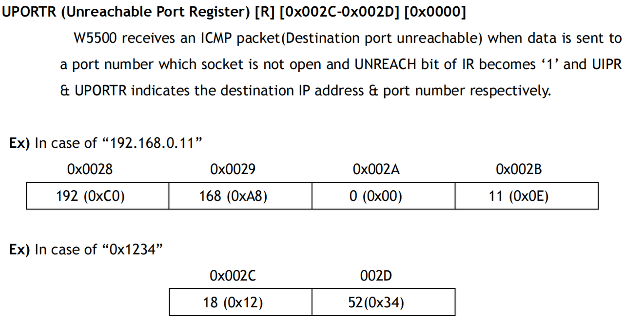
PHYCFGR W5500 PHY Configuration Register Configure PHY operating‑modes and trigger PHY reset.

VERSIONR W5500 Chip‑Version Register Show silicon‑version identifier of chip.

For full register definitions and operation details, refer to section 4.1 in original document: http://www.boccn.com.cn/artupfile/2014-02-11/02014021111343613482.pdf
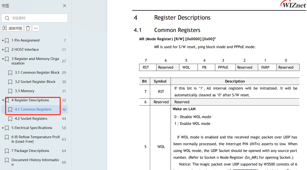
4.3 Socket Register Block
W5500 provides 8 communication channels controlled by Socket‑n register blocks (0 ≤ n ≤ 7). Target socket‑n is selected by BSB[4:0] in SPI frame.
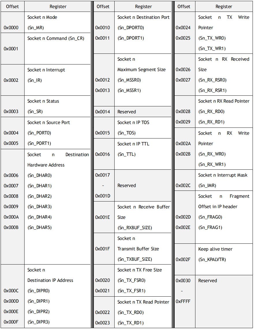
Brief function summary for each Socket‑n register block is given in following figures.
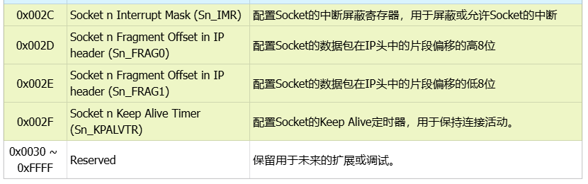
For full register definitions and operation details, refer to section 4.2 in original document: http://www.boccn.com.cn/artupfile/2014-02-11/02014021111343613482.pdf
4.4 Memory Organization
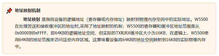
W5500 has 16 KB TX memory and 16 KB RX memory used as socket buffers.
TX Memory Allocation By default each socket TX buffer is assigned 2 KB (2 KB × 8 = 16 KB). Buffer sizes can be re‑configured via register Sn_TXBUF_SIZE. Buffers are allocated sequentially. Sum of all socket TX‑buffer sizes must not exceed 16 KB to avoid transmission errors.
RX Memory Allocation By default each socket RX buffer is assigned 2 KB (2 KB × 8 = 16 KB). Buffer sizes can be re‑configured via register Sn_RXBUF_SIZE. Buffers are allocated sequentially. Sum of all socket RX‑buffer sizes must not exceed 16 KB to avoid receive errors.
Address Mapping TX and RX buffers use 16‑bit offset addresses (0x0000 ~ 0xFFFF) mapped onto 16‑KB physical memory. Registers Sn_TX_WR and Sn_RX_RD manage buffer pointer positions.
4.5 VDM Variable‑Data‑Length Mode Read / Write Operations
4.5.1 Write Data
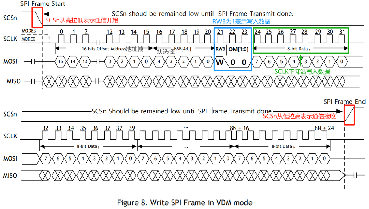
VDM Mode
RWB bit set to '1' for write operation. OM[1:0] set to '00' inside SPI‑frame control phase to select VDM.
SPI Frame Transfer Procedure
SCSn signal: host drives SCSn from high to low before SPI transaction to select W5500 and prepare for data transfer. MOSI signal: host shifts‑out all data bits to W5500, synchronized with falling edge of SCLK. SCLK signal: serial clock for bit‑level synchronization.
Transaction Completion
After SPI‑frame data transfer completes, host drives SCSn from low to high to terminate transaction. Sequential burst‑write is supported while SCSn stays low and data‑phase continues.
4.5.2 Read Data
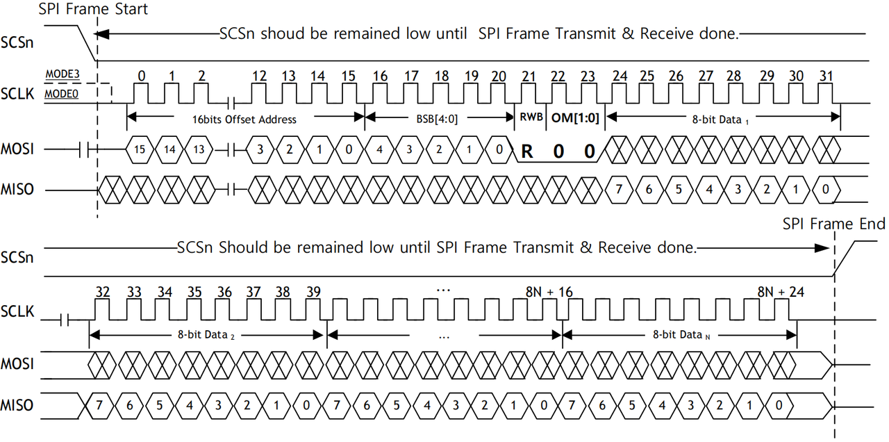
RWB bit is set to '0' for read operation. Transaction start‑stop sequence is same as write operation. Host receives data bits over MISO line, sampling at rising edge of SCLK.
4.6 FDM Fixed‑Data‑Length Mode Read / Write Operations
FDM mode applies when host cannot control SCSn signal. SCSn must be permanently tied low to GND. SPI‑bus cannot be shared with other SPI peripherals. Data‑phase byte‑count is controlled by OM[1:0] value ('01' / '10' / '11') supporting 1‑byte, 2‑byte or 4‑byte transfers.
4.6.1 Write Data
Example for 1‑byte and 2‑byte write transactions:
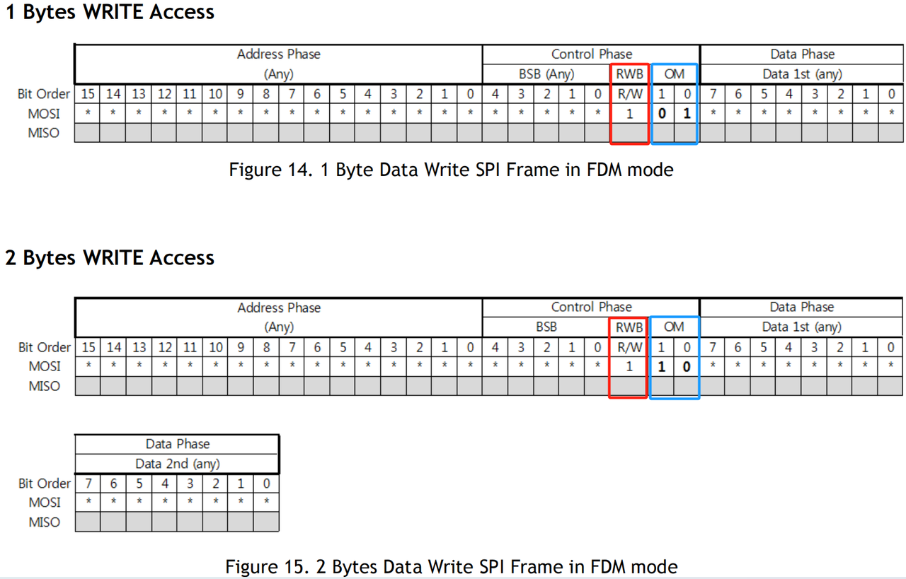
RWB set to '1' for write; OM bits select transfer byte‑count.
4.6.2 Read Data
Example for 1‑byte and 2‑byte read transactions:
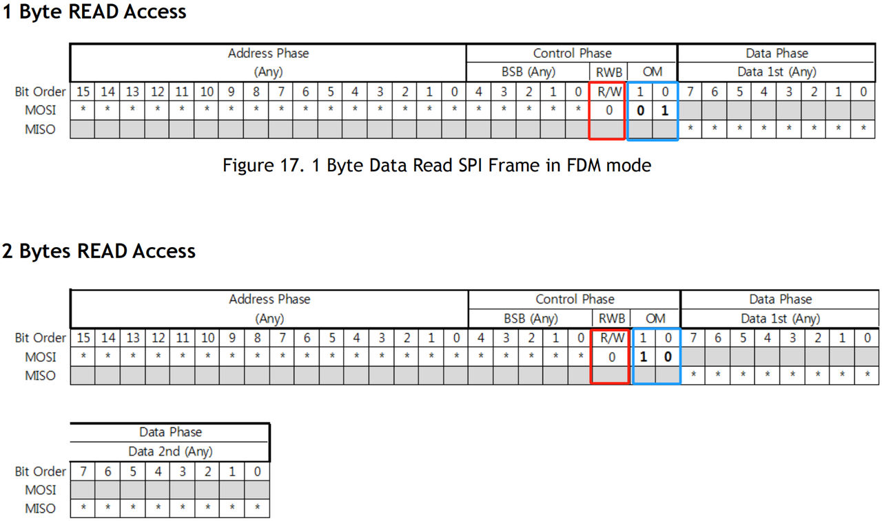
RWB set to '0' for read; OM bits select transfer byte‑count.