Understanding Chip System Block Diagrams: Start with the RP2040's "Miniature Factory"
This article explains how to learn chips via block diagrams and introduces each functional module of RP2040 with a vivid miniature factory analogy.
COMPONENTS
PROJECT DESCRIPTION
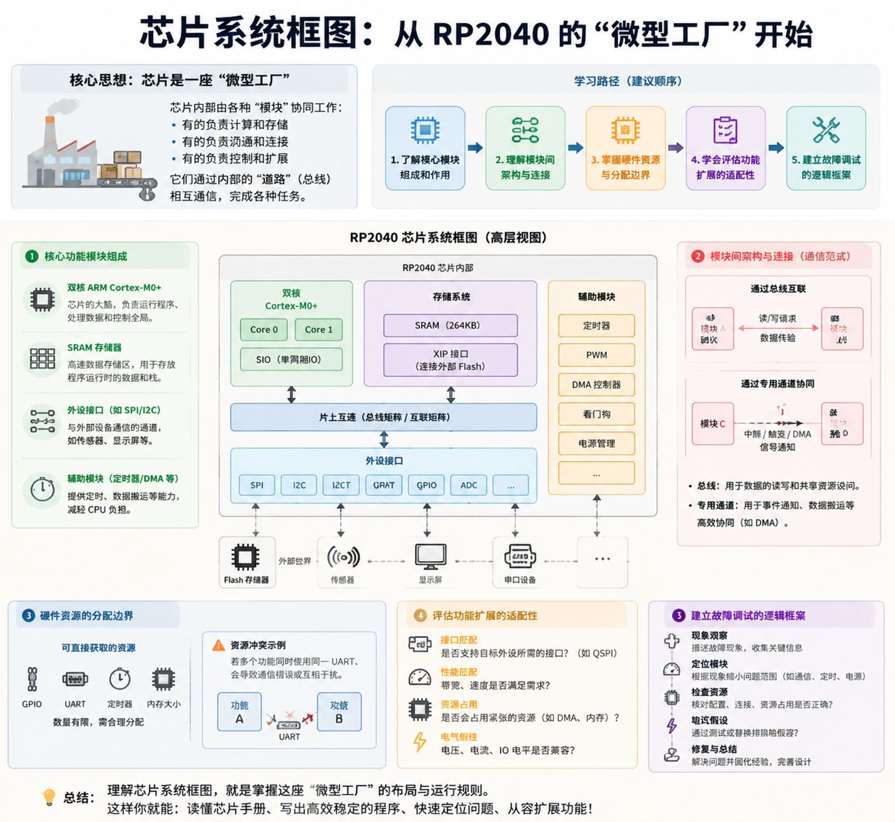
For any chip, the block diagram serves as the core starting point for learning — it acts as the chip's "architecture specification", helping you build a systematic understanding (rather than a scattered list of functions), which is the universal approach to learning all chips. Through the block diagram, you can first grasp the information from the following general dimensions before delving into specific functions:
Clarify the composition of core functional modules: Whether it is a microcontroller, processor or dedicated chip, the block diagram will clearly divide the arithmetic core (such as the dual cores of RP2040), storage units (such as SRAM), peripheral interfaces (such as SPI/I2C), and auxiliary modules (such as clock/power supply), allowing you to quickly know "what basic components the chip contains" — this is the "component list" for subsequent learning.
Master the architectural logic between modules: The block diagram presents the hierarchical relationships of each module (for example, the core is the core control layer, and the peripherals are the external interaction layer) and communication links (for example, the bus is the interconnection hub between modules), helping you understand how the various components of a chip work together — for instance, the core of all chips accesses memory and controls peripherals through the bus, which is the general logic of chip operation (corresponding to the Bus Fabric interconnection of RP2040).
Define the allocation boundaries of hardware resources: Key resources of the chip (such as the number of GPIOs, memory size, and peripheral types) can be directly obtained through the block diagram, which is a prerequisite for subsequent hardware design and program development — for example, by knowing how many UARTs a chip has, one can determine how many serial port devices it can connect simultaneously (corresponding to the 2 UARTs and 30 GPIOs of the RP2040).
Evaluate the adaptability of function extensions: The programmable modules (such as the PIO of RP2040) and expansion interfaces (such as QSPI) in the block diagram will indicate whether the chip supports custom functions and external devices, which is the core basis for judging whether the chip can adapt to specific scenarios — for example, the block diagram of a general-purpose microcontroller includes programmable modules, while the block diagram of a dedicated chip mostly consists of fixed peripherals.
Establish a logical framework for fault debugging: When encountering problems subsequently, you can quickly identify the failure domain based on the module division of the block diagram (e. g., for communication anomalies, first check the peripherals and buses; for calculation errors, first check the core) — this is a universal approach for debugging all chips.
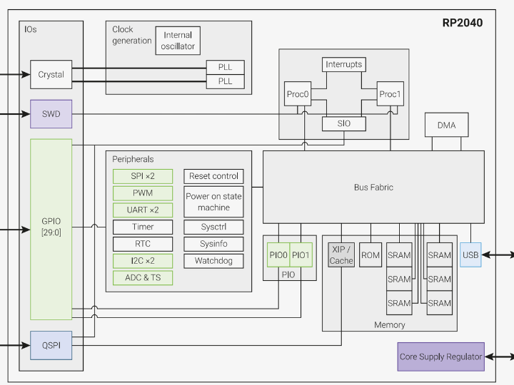
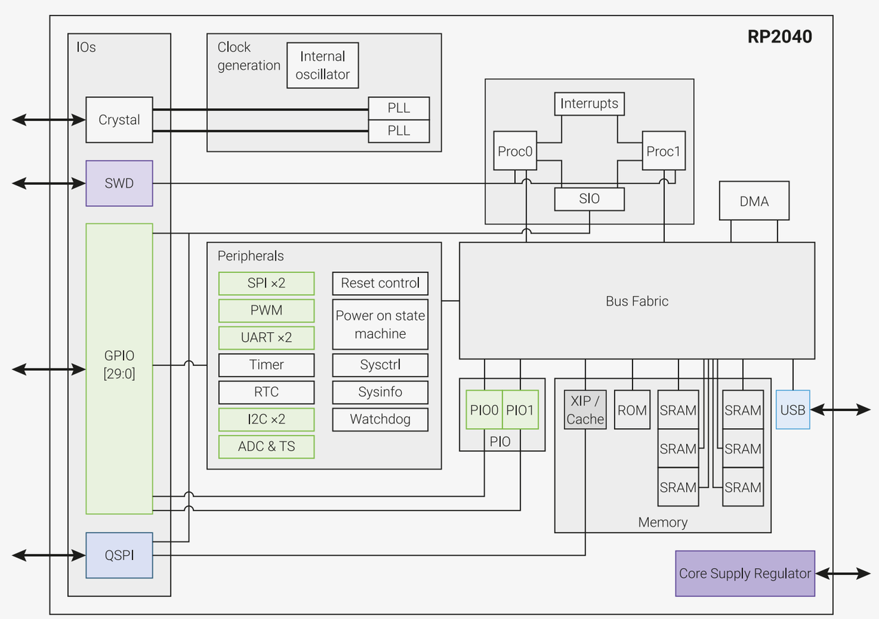
The RP2040 features dual M0+ processor cores, DMA, on-chip memory, and peripheral blocks connected via an AHB/APB bus structure:
Figure 2.3 Internal Architecture Block Diagram of the RP2040 Chip
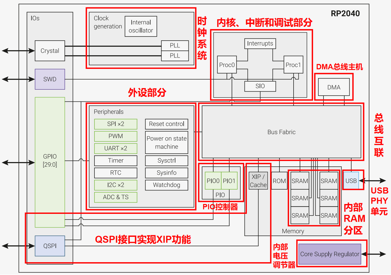
We can think of a chip as a "miniature factory", where each module in the diagram corresponds to a distinct "workshop / post": some are responsible for computation, some for data transmission, and others for interfacing with external devices. These posts work in tandem to enable the chip to fulfill tasks such as control and arithmetic operations. Below, we will explain the function of each "post" according to the partitions in the diagram:
Clock System: It acts as the "metronome" of a factory — responsible for generating a stable "time rhythm"(for instance, internal oscillators and external crystal oscillators provide the basic beat, while the PLL module speeds this beat up to 133MHz), ensuring that all modules operate in a synchronized rhythm (for example, the timed 1-second flashing of an LED relies entirely on this beat to keep time).
Kernel, Interrupt and Debugging Section: It functions as the "core workers" of the factory — Proc0 and Proc1 are the two "workers"(dual-core) responsible for executing programs and handling core tasks; SIO serves as the "workers' tool room" that enables data exchange between the two workers; Interrupts act as the "emergency caller" that can interrupt the workers' ongoing tasks to prioritize urgent ones when sudden tasks occur (such as unexpected sensor triggering); SWD is the "supervisor interface" that allows checking the workers' working status to identify the root cause of task errors.
DMA bus master: it acts as the "porter" in a factory — it handles data transfer for core processing units (such as moving sensor data from peripherals to memory), freeing the core units from having to perform such routine tasks on their own so that they can focus on processing core tasks and thus improve overall efficiency.
Bus Fabric: serves as the "internal pathway" of the factory — all communication and data transmission between modules are carried out via this pathway, ensuring efficient interconnection between all workstations.
Internal RAM Partition: It acts as the "temporary warehouse" of the factory — the 264KB SRAM is divided into 6 "small warehouses", which can store different temporary data simultaneously (for example, Worker A uses Warehouse 1, while the porter uses Warehouse 2), thus preventing space conflicts and improving data access efficiency.
Peripheral Section: serves as the "external interface" of the microcontroller. It consists of modules including SPI/I2C/UART (the "communication interfaces" for interacting with external devices), PWM (the "regulator" for dimming lights or controlling motors), and ADC&TS (the "measuring instrument" for detecting voltage and temperature), which are responsible for connecting and interacting with external components such as sensors and LEDs.
PIO controller: it serves as the "universal tool bench" for factories — capable of customizing interface functions (such as emulating SD cards and VGA interfaces) to expand the peripheral capabilities that the original chip does not have.
QSPI interface implementing XIP functionality serves as the "direct access channel from the external warehouse" for the factory: it connects to external flash memory (equivalent to an "external large warehouse") via the QSPI interface, and the XIP feature enables the chip to read programs directly from the external warehouse without first transferring them to the internal temporary storage, thus saving internal space.
USB PHY Unit: serves as the "USB express interface" of the factory — it is responsible for communicating with external USB devices (computers, USB flash drives) to enable program downloading and data transmission.
Internal Voltage Regulator: It acts as the "power supply stabilizer" of the chip — it stabilizes the externally input voltage and converts it into the 1.1V voltage required by the chip core, ensuring stable power supply for all modules.
Figure 2.4 Analysis Diagram of Internal Architecture Partitioning of RP2040 Chip
A brief description is as follows:
XIP / Cache : The microcontroller connects to an external NOR QSPI FLASH via a dedicated SPI, DSPI or QSPI interface to implement the XIP (eXecute In Place) function, and a small cache can improve the performance of typical applications;
SWD Debug Interface: The SWD debug interface is connected to the core;
Internal SRAM Partition: The internal SRAM can store code or data. It is configured as a single 264kB region, but physically divided into 6 banks to enable simultaneous parallel access from different host buses, for example, the CPU can access one bank while the DMA accesses other banks;
GPIO Ports and Peripherals: GPIO pins can be directly driven, or work with peripherals to implement functions to reuse such as SPI, I2C and UART
PIO Controller: The flexible and configurable PIO controller can be used to provide various IO functions
USB PHY Unit: A USB controller with an embedded PHY can be used to provide FS/LS host or device connections under software control
Clock System: Two PLLs (Phase-Locked Loops) provide a fixed 48MHz clock for USB or ADC, as well as a flexible system clock up to 133MHz.
Internal Voltage Regulator: An internal voltage regulator is provided to supply the 1.1V core voltage
DMA Bus: The DMA bus master can be used to offload repetitive data transfer tasks from the processor
Kernel Part: Two fully symmetric processing cores, Proc0 and Proc1