Understand UF2 in 1 Minute: The "Drag-and-Drop" Magic for Flashing Firmware on Pico, Full Principle
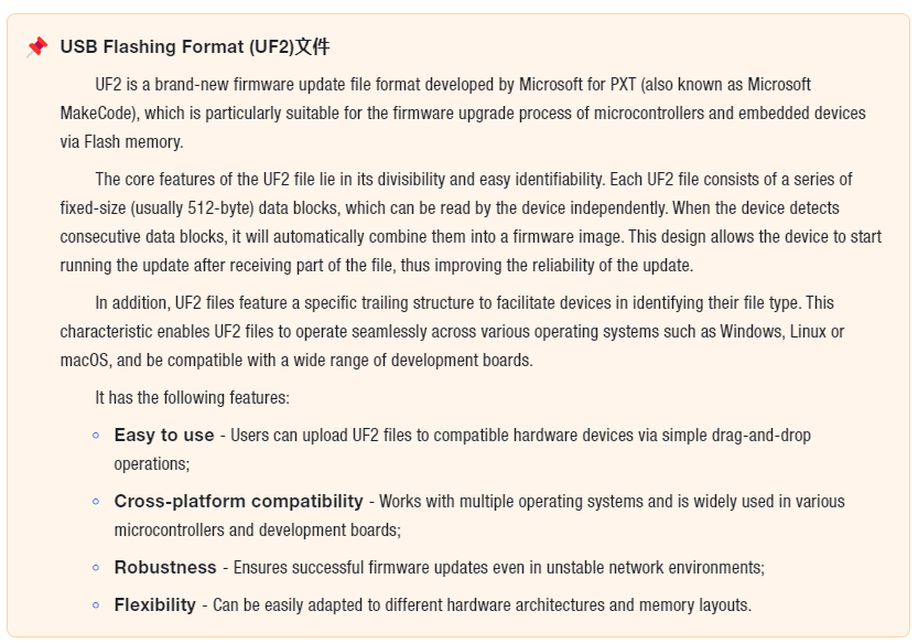
UF2 (USB Flashing Format) developed by Microsoft is used for Raspberry Pi Pico firmware.
COMPONENTS
PROJECT DESCRIPTION
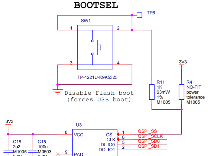
Figure 1.9 BOOT Mode Selection Circuit
This circuit comprises two key functional modules of the Pico: one is the BOOT mode selection circuit that controls the "startup state", and the other is the Flash memory circuit that stores programs — the former helps you switch between the "run existing program" and "load new program" states, while the latter acts as the Pico's "built-in small hard drive" for storing programs. Their specific functions are detailed as follows:
The onboard 2MB QSPI flash memory can be (re-) programmed via the serial wire debug port or through a special USB mass storage device mode.
The upper part is the BOOT mode selection circuit. The startup mode switching button is connected in series with a 1kΩ resistor to the QSPI_SS pin of the RP2040. This series resistor ensures that the content in the Flash will be executed when the reset button is pressed in BootLoader mode.
When the RP2040 is powered on, the QSPI_SS pin will automatically default to a pull-up state. The RP2040 checks the value of this I/O during the boot process; when QSPI_SS is at logic 0, the RP2040 enters the BootLoader mode.
When the BOOTSEL button is not pressed, upon reset or power-up: the device enters normal mode, and the MCU boots the stored program from Flash.
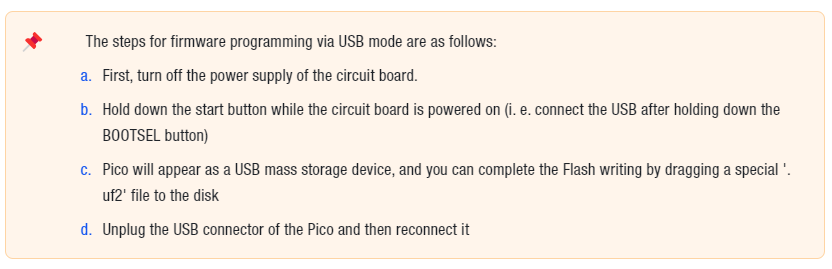
When the BOOTSEL button is pressed during reset or power-up, the MCU enters the "program loading" BootLoader mode, at which point the Pico will appear as a USB flash drive on the computer, and the firmware can be updated simply by dragging and dropping a uf2 format program file into it.
During a short period at power-on, the state of the QSPI_SS pin cannot be guaranteed, which can be ensured by adding a pull-up resistor. For the W25Q128 Flash memory, an external pull-up resistor is unnecessary, so it is marked as NO-FIT and can be omitted during soldering.
Below is the Flash memory circuit, whose power supply operates at the same voltage as the 3.3V power pin of the chip. The pins of the W25Q128 are connected to the QSPIx pins of the RP2040. Place 2.2uF and 100nF filter capacitors near the power pin (VCC) of the Flash memory W25Q128 to provide a stable 3.3V power supply for the W25Q128JVSIQ.