Embedded 101: Unusable Registers in MCUs – TBMan Only Serves as Identifier
This article introduces RP2040 Sysinfo identification registers, Syscfg system configuration registers and the simulation-only TBMan module.
COMPONENTS
PROJECT DESCRIPTION
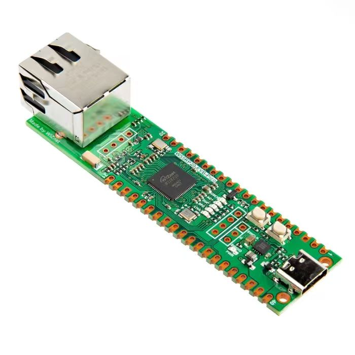
【Preliminary Note】The original hardware example in this article was written based on the RP2040. The actual hardware used in this hands-on demonstration features the W55RP20 as the main controller chip. The circuit logic and UF2 flashing operation principles are universally applicable, with only the main controller model differing. The original chip model mentioned in the circuit descriptions below is provided for reference purposes only.
1. Sysinfo Register
Sysinfo registers can be understood as the "About This Device" information area of a chip: just like the page on a mobile phone where you can check the model and version, they specifically store the basic identity information of the chip, and software can know which chip it is running on and which version the chip is by reading these registers.
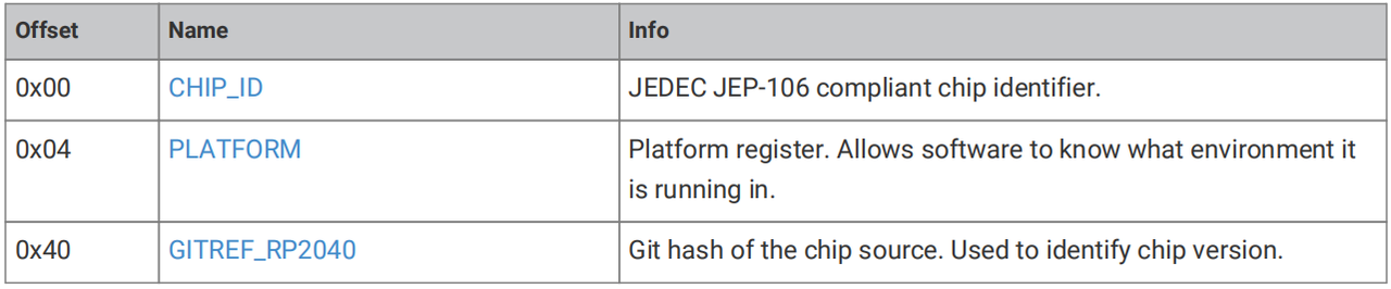
The sysinfo module is a region in the chip that stores "basic system information". Its registers start at address 0x40000000 and contain 3 core pieces of information:
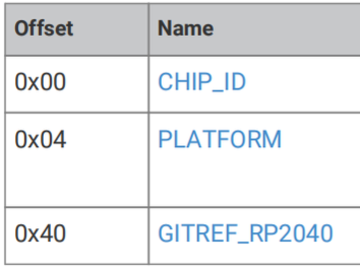
CHIP_ID (Offset 0x00): The "standard identification number" of the chip, which complies with the JEDEC industry specification; the software can identify the currently used chip model by reading this register.
PLATFORM (Offset 0x04): This is the "running platform identifier" of the chip. When reading this register on the RP2040, the result is always 1, and the software uses it to confirm its operating environment;
GITREF_RP2040 (offset 0x40): This field represents the "version hash" of the chip, which is equivalent to the production version number of the chip. Different batches and versions of chips can be distinguished by this Git hash.
sysinfo registers start at the base address 0x40000000:
The Syscfg register can be regarded as the "system-level configuration panel" of a chip — similar to the BIOS settings on a computer, it is specifically designed to adjust the parameters of core components such as the processor, debug interface, and memory, so as to enable the chip to adapt to different operating and debugging requirements. All these settings are stored in registers starting at the address 0x40004000.
The system configuration block controls various chip settings, including:
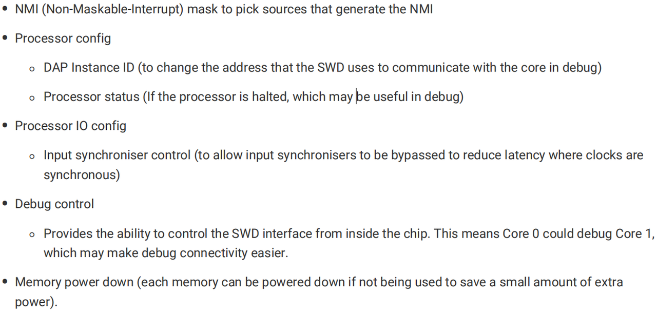
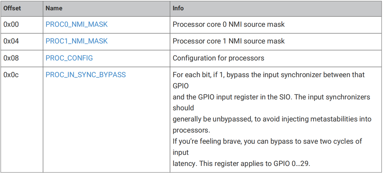
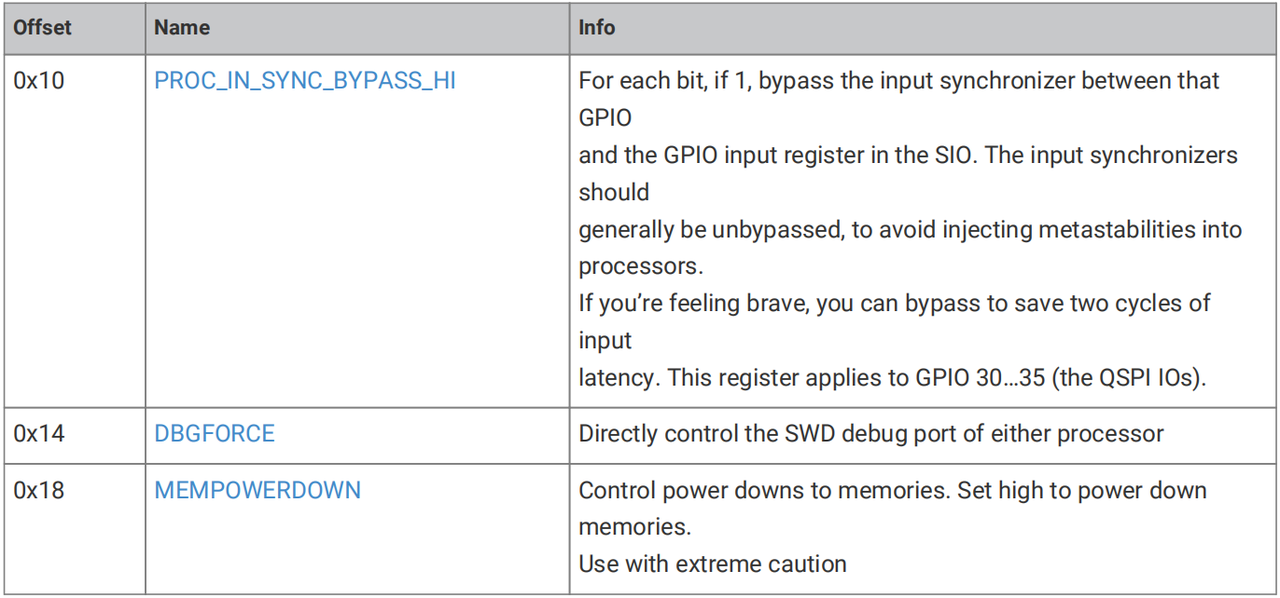
Figure 2.55 List of Syscfg Register Function Descriptions
The system configuration block serves as the "core parameter adjustment zone" of the chip, which can control the following key settings:
NMI Emergency Interrupt Mask: NMI stands for "Non-Maskable Interrupt", which refers to an urgent alert that cannot be ignored. This setting is used to select which signals can trigger this alert (for example, it requires mandatory response when a serious chip failure occurs).
Processor Configuration:
Modify the communication address (DAP instance ID) of the debug interface to facilitate the connection of debug tools to the core;
Check whether the processor is "stuck"(processor status), which enables quick problem locating during debugging.
Processor IO Configuration: Controls the "rhythm aligner (synchronizer)" for GPIO input — if the external signal is consistent with the chip clock rhythm, turning off the synchronizer can reduce signal latency (but generally do not turn it off, as it easily leads to data errors).
Debug Control: The chip has an internal mechanism to control the debug interface. For example, Core 0 can directly debug Core 1 (similar to an "internal remote assistance function"), which allows troubleshooting issues on another core without connecting an external debugger.
Memory power-off: Unused memory can be powered off to save power (but special caution is required, as data stored in the memory will be lost after power-off).
The base address of the system configuration register is 0x40004000.
Corresponding register functions (refer to the table):
PROC0/PROC1_NMI_MASK: controls the trigger sources of non-maskable interrupts for core 0 and core 1 respectively;
PROC_CONFIG: stores the configuration parameters of the processor;
PROC_IN_SYNC_BYPASS / PROC_IN_SYNC_BYPASS_HI: control the input synchronizers for regular GPIOs (0~29) and QSPI group GPIOs (30~35) respectively;
DBGFORCE: controls the debug interfaces of the two cores;
MEMPOWERDOWN: Controls memory power-off (use with caution, as data loss will occur).
3. TBMAN Test Bench Manager
TBMan (Test Bench Manager) is a "testing auxiliary tool" used in the chip development and simulation phase, which can be analogized to the "beta-exclusive debugging feature" for software: during the chip design and simulation verification stage, tools are required to control the test environment and check whether functions operate properly, and that is exactly what TBMan is designed for; however, once the chip is actually manufactured, this tool becomes obsolete, leaving only an "identifier" to prove that the chip is a genuine product.
The TBMAN registers start at the base address 0x4006c000.
Figure 2.58 Description of TBMAN Test Bench Manager Registers
However, on mass-produced chips, TBMan serves virtually no practical purpose, with only one PLATFORM register (at address 0x4006c000, offset 0x0) retained to indicate "this is a physical chip", and this identification function overlaps with the platform identifier in the earlier Sysinfo register.