



SD‑Card Deep Dive: Hardware, Protocol, MicroPython Driver & Filesystem Mount
SD‑card hardware, protocol, driver and filesystem mounting.
1.SD card basic knowledge SD‑card communication protocol dissection: CMD commands and their response message structures
1.1 SD‑card introduction and classification
An SD card is a removable storage device widely used in digital devices. It features compact size, low power consumption and large‑capacity storage. It is mainly used for storing data, music, video, images and other content, and is commonly found in mobile phones, cameras, tablets and embedded hardware.
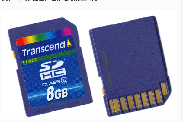
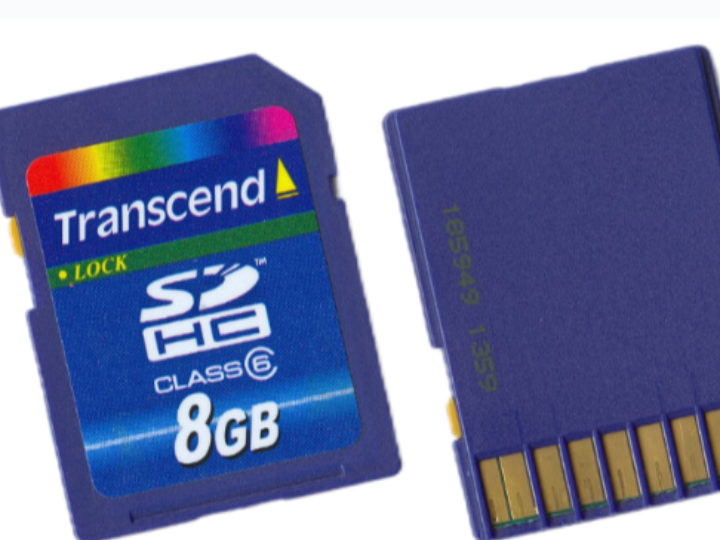
According to physical dimensions, SD cards fall into these categories:
Standard SD card: dimension 32mm x 24mm x 2.1mm, used in larger‑size equipment such as cameras and voice recorders
miniSD card: dimension 21.5mm x 20mm x 1.4mm, rarely seen today, mainly deployed on early‑generation mobile phones
microSD card, also known as TF card: dimension 15mm x 11mm x 1mm. Widely used in cell phones, drones, Raspberry‑Pi and other small‑form‑factor devices. It can be adapted into a standard SD card with an SD‑card adapter.
Based on capacity and protocol specifications, SD cards are divided into the following types:
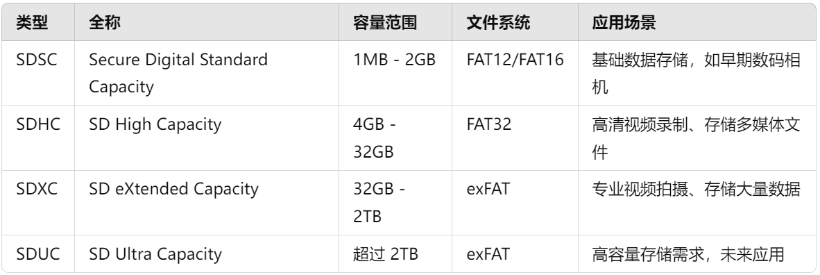
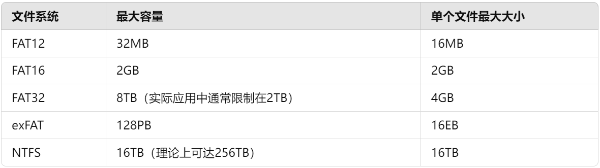
Note that the maximum capacity supported by each file system varies across host devices:
Two basic supplementary concepts:
Maximum capacity: the upper total storage‑space limit that a given file system can manage (for example FAT12 can handle devices up to 32 MB).
Maximum single‑file size: the upper size limit for one individual file (for example FAT32 files cannot exceed 4 GB, which may be insufficient for storing large‑size movies).
FAT12 and FAT16: intended for small‑capacity storage media, suited for legacy applications.
FAT32: widely adopted for SDHC cards and other mid‑size storage devices, subject to the 4 GB single‑file size restriction.
exFAT: designed for flash drives and high‑capacity storage media, supports larger files and total capacities, suitable for SDXC cards.
NTFS: primarily used for Windows operating‑system environments, supports large‑size files and high capacities but is seldom used on SD‑card media.
SD‑card speed classes represent guaranteed minimum write performance (sufficient write speed prevents stuttering during operation). Common speed classes for different use‑cases are listed below:
Class 2: minimum write speed 2 MB/s, suitable for standard‑definition video recording
Class 4: minimum write speed 4 MB/s, suitable for HD‑video recording
Class 6: minimum write speed 6 MB/s, suitable for FHD full‑high‑definition video recording
Class 10: minimum write speed 10 MB/s, for high‑definition video and continuous burst shooting
UHS‑II: delivers much higher transfer rates with write speeds above 30 MB/s.
1.2 SD‑card physical structure and operating principle
An SD card mechanically consists of plastic housing, metal contact pins, flash‑memory chips and an on‑card controller. Its housing is built from robust plastic to resist physical shock and environmental stress.
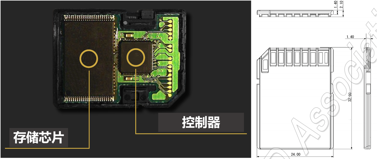
Think of an SD card as a USB‑flash‑drive with an on‑board intelligent manager. It performs work via these functional units:
Storage core: stores user data inside NAND flash memory, similar to the storage chips inside smartphones.
Intelligent manager (controller):
Receive commands sent from external hosts, for example “read file XX”, then fetch corresponding data from flash memory.
Manage stored data using file‑system standards such as FAT32 / exFAT. The previously‑introduced VFS virtual‑file‑system layer can interface with this logic.
Implement wear‑levelling technology: distribute write operations across different flash regions, preventing premature wear caused by repeated writes to a single block.
Built‑in error correction: automatically detect and repair minor data corruption to avoid read errors.
Multiple metal contact pins sit on the bottom side of the SD‑card, responsible for data transmission, power‑supply and signal control. Standard SD cards have 9 pins; microSD cards feature 8 pins.
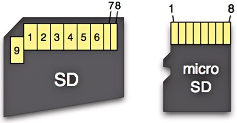
The 9 pins of a standard SD‑card include four data‑transmission pins DAT0~DAT3, command pin CMD, ground pin VSS and power‑supply pin VDD. Standard SD‑cards also carry a physical WP (Write Protect) write‑protection switch.
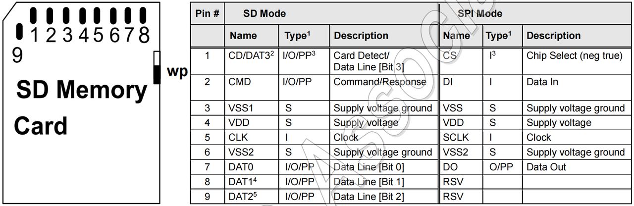
Before describing pin functions, note there are two primary SD‑card operating modes:
SD Mode: high‑speed mode with many signal pins and relatively complex communication logic, commonly implemented in consumer hardware such as smartphones and cameras.
SPI Mode: fewer required pins and simpler communication flow. This is the typical choice for embedded‑board SD‑card interfacing, and is the main focus for beginners.
Below is the mapping of each pin’s function under the two different modes:
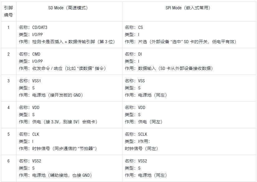
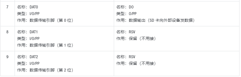
Abbreviations used in pin‑type descriptions:
I: Input; SD‑card receives signals from external host hardware.
O: Output; SD‑card transmits signals to external host hardware.
I/O: Bidirectional; supports both signal receive and signal transmit.
S: Power or ground; power‑supply connection or ground reference.
A mechanical write‑protect slider sits on the side of standard SD‑cards. Internally the card samples the logic level of a dedicated pin, normally pin 8.
When the WP pin is pulled low (detects the corresponding logic level), write operations are locked out and only read access is permitted.
Moving the physical switch back restores full read‑write capability.
Beyond pins, controller and NAND flash, SD‑cards contain multiple on‑card registers storing card identity, status, configuration and operating‑condition parameters. See the diagram below:
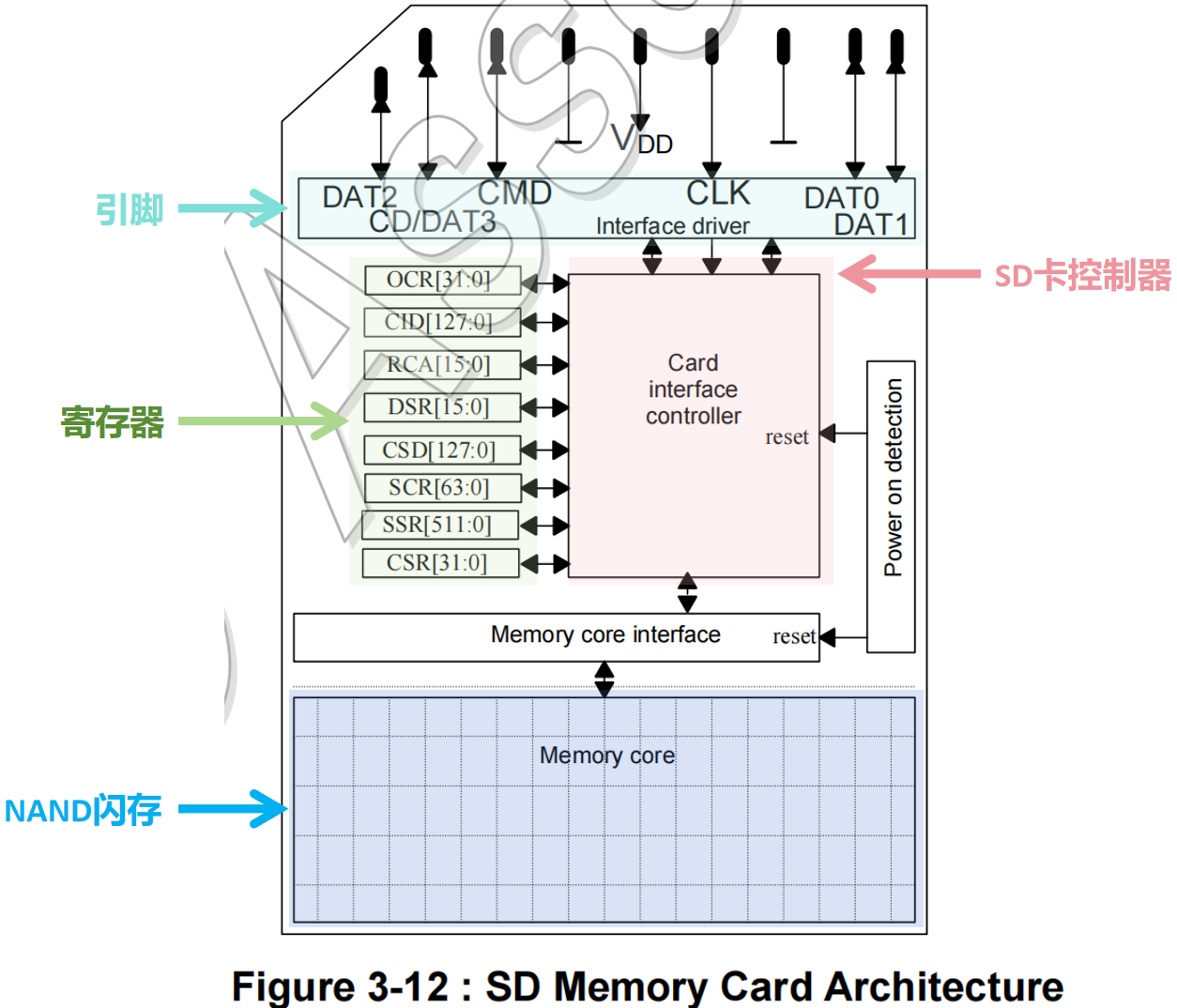
The internal SD‑card architecture operates as layered‑cooperating components with well‑defined responsibilities:
Pins and interface driver: corresponds to the “pin” section in the diagram. Acts as the physical‑link interface between SD‑card and external host such as development boards, responsible for command delivery, data transfer and power‑supply routing.
Card interface controller: the intelligent central control unit of the SD‑card. Core responsibilities:
Accept incoming host commands such as “read file XX” or “query card information”.
Read and modify values stored inside on‑card registers.
Manage read‑write operations targeting NAND flash storage.
Execute wear‑levelling and error‑correction algorithms to preserve card lifespan and guarantee data integrity.
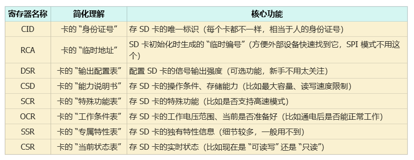
Registers: corresponds to the register block in the diagram. Stores critical information including card identity, operational status and hardware capabilities. The controller continuously reads these registers, and external hosts can also retrieve register content by sending dedicated commands.
Memory core (NAND flash): the actual storage medium of the SD‑card. User payloads including photos and files reside here. These storage cells are fully managed by the on‑card controller.
Key registers and their functions are shown below:
Co‑operation workflow between external host MCU and SD‑card:
- The external host sends commands to the SD‑card controller via physical pins, for example “read your identification information”.
- The controller fetches required data from target registers such as the CID register, then returns information to the host over the pin interface.
- For data‑read or data‑write operations, the controller allocates storage space and performs read / write access against NAND flash according to incoming commands.
- Throughout this process the controller applies wear‑levelling (distribute writes across flash cells to prevent accelerated wear) and error correction logic to protect the SD‑card hardware and stored user data.
1.3 SD‑card operating modes
Interaction between host hardware such as development‑boards or mobile phones and SD‑cards can be compared to plugging a new USB drive into a smartphone.
Card‑identification mode: handshaking and initialisation sequence between host and newly‑inserted storage media.
Data‑transfer mode: after handshaking completes, the phase where host writes files to or reads files from the storage medium.
SD‑card operation consists of two major phases: Card Identification Mode and Data Transfer Mode. Under Card Identification Mode the host identifies and initialises the SD‑card to prepare it for data‑transfer operations. Data‑Transfer Mode is the phase for actual file‑read and file‑write work.
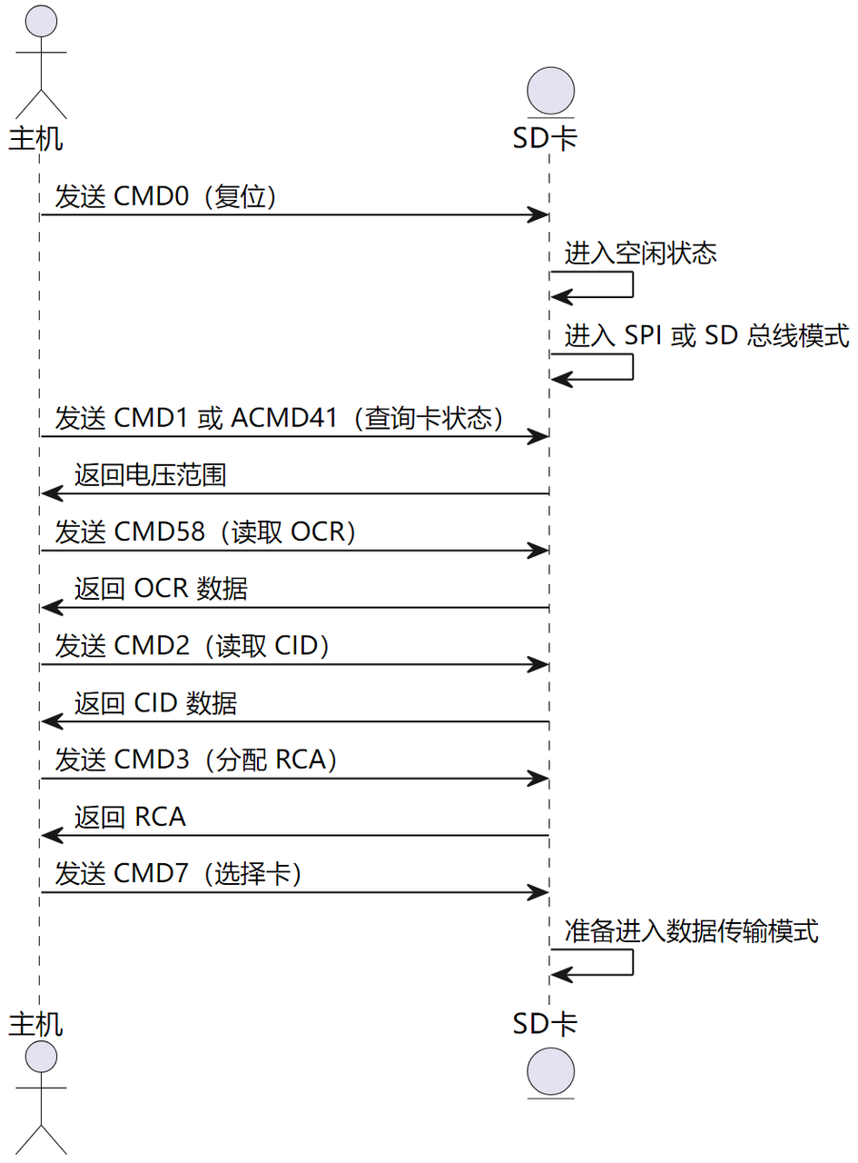
In the flow chart, Idle / Ready / Ident represent SD‑card operational states. CMD0 / CMD8 are commands transmitted from host to SD‑card. The full workflow is described as:
- Initial phase: Idle State
- After card insertion or power‑on reset, host issues CMD0 reset command. Conceptually equivalent to host sending: “Hello, please reset and get ready for communication.”
- The SD‑card enters Idle state, selects its operating mode (SPI or SD‑bus mode), and waits for further host commands.
- Voltage validation: issue CMD8
- Host sends CMD8, conceptually asking: “Do you support our supply‑voltage level?”
- If the SD‑card does not support the present voltage, it falls back to Idle state. If supported, execution proceeds onward.
- Check card readiness: issue ACMD41
- Host transmits ACMD41 command, equivalent to querying: “Are you ready for operation?”
- When ready, SD‑card enters Ready State. If not ready, it returns busy status and host retries the query after a short delay.
- Request card identity: issue CMD2
- Host sends CMD2: “Return your unique identifier stored inside the CID register.”
- SD‑card transitions into Identification State and transmits CID content including manufacturer ID and serial number back to host.
- Assign temporary card address: issue CMD3
- Host sends CMD3: “I assign you a temporary RCA address for subsequent addressing.”
- SD‑card enters Stand‑by State, holding this RCA identifier for fast future host addressing.
- Select target card: issue CMD7 and enter Data Transfer Mode
- Host issues CMD7: “You are selected, prepare for data transmission.”
- SD‑card exits Card‑Identification Mode and switches to Data‑Transfer Mode, enabling file read‑write access.
Additional special‑case workflows:
Legacy MMC multimedia‑cards use the CMD1 initialisation sequence instead of CMD8 / ACMD41.
CMD15 is the deselect‑card command. Conceptually “I will stop accessing you.” The card reverts back to its prior state.
1.4 SD‑card communication protocol and command‑response model
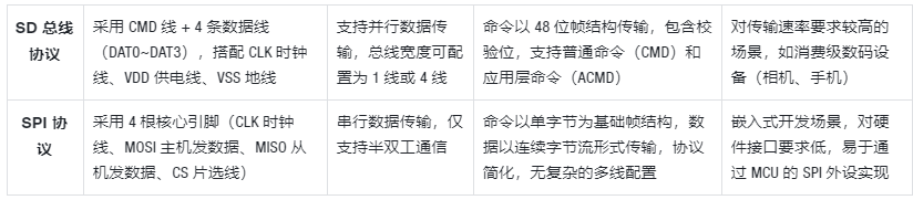
Two main communication protocols exist for SD‑cards: SD‑bus protocol and SPI protocol.
SD‑bus protocol: uses multiple data lines, typically four data lines, for parallel data transfer. Supports multiple speed grades including SD, SDHC, SDXC. Operations are triggered by sending CMD‑prefixed commands with associated parameters.
SPI protocol: uses four hardware pins CLK, MOSI, MISO, CS for serial‑mode transmission. Commands are sent as single‑byte frames; data is streamed as byte sequences.
1.4.1 Command‑response model inside SD‑bus protocol
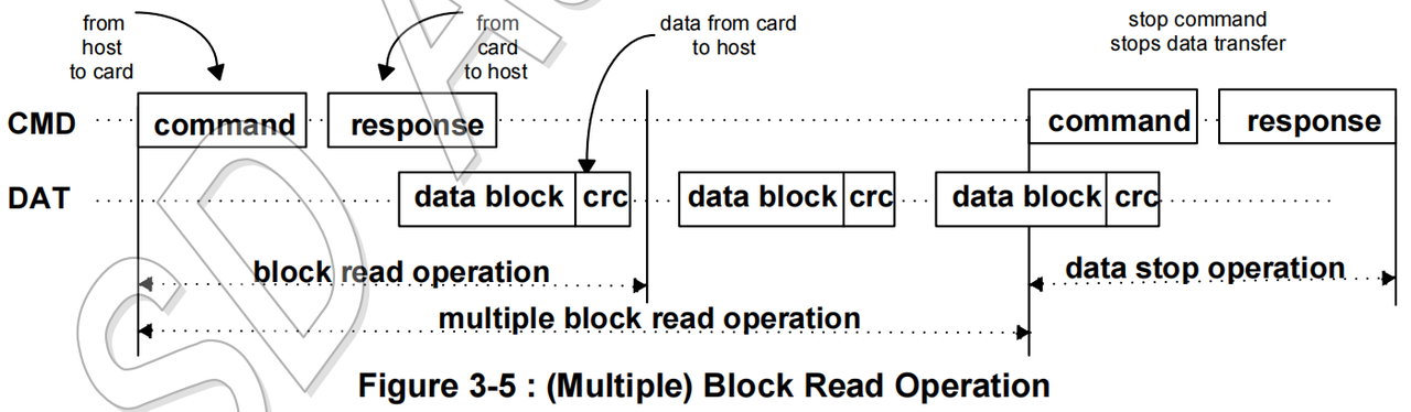
SD‑card communication follows a command‑response pattern. The host sends commands to trigger specific operations, and the SD‑card generates corresponding responses. Commands CMD and responses RESPONSE are transmitted serially over the CMD signal line. Payload DATA is transferred via DAT data lines. Command signalling and data signalling are independent channels.
The format of CMD command frames is shown below, containing start bit, transmission bit, command content (command number plus address or parameters), and stop bit.
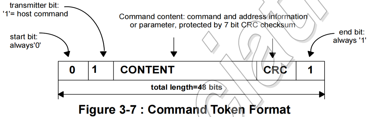
SD‑bus command frames have a fixed total length of 48 bits. Field layout ordered from highest bit down to lowest bit:
Start bit (1bit): hard‑coded value 0, marks beginning of a command frame.
Transmission bit (1bit): hard‑coded value 1, indicates frame direction: host‑to‑SD‑card command.
Command index (6bit): specifies command type. CMD0 corresponds to value 0x00, CMD2 corresponds to value 0x02.
Command parameter (32bit): carries configuration values dependent on command type; may include memory address, capacity arguments, status masks and so forth.
CRC check bits (7bit): CRC7 checksum computed across preceding 41 bits, guarantees correct command reception.
Stop bit