RP2040 PIO Programming Model & FSM Principles: Hardware to Working Logic
RP2040 PIO state‑machines use pioasm instructions, shift registers and side‑set, with GPIO mapping and IRQ flags for multi‑state‑machine synchronization.
COMPONENTS
PROJECT DESCRIPTION
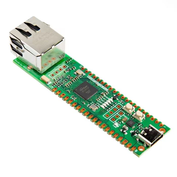
【Preliminary Note】The original hardware example in this article was written based on the RP2040. The actual hardware used in this hands-on demonstration features the W55RP20 as the main controller chip. The circuit logic and UF2 flashing operation principles are universally applicable, with only the main controller model differing. The original chip model mentioned in the circuit descriptions below is provided for reference purposes only.
Programming Model of PIO and Working Principle of finite-state machine
The programming model of PIO peripherals shares commonalities with general-purpose processors: both implement functions by sequentially executing pre-written programs, and can complete data interaction via the DMA/interrupt system and realize state control by reading and writing control registers. Different from general-purpose processors, however, PIO is a hardware subsystem designed specifically for input and output scenarios, so it features strong timing determinism and high operation precision, and is deeply bound to fixed-function hardware such as GPIO and DMA.
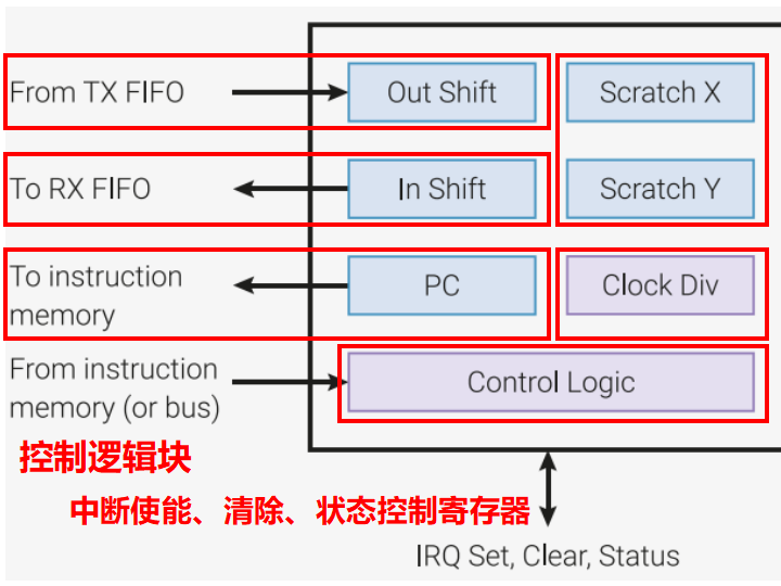
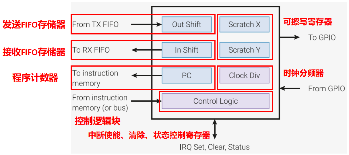
The core of PIO's function implementation lies in the 4 independent finite-state machines it contains. Each finite-state machine features a highly integrated hardware structure (corresponding to the finite-state machine structure diagram), and its composition and working principle are as follows:
Including:
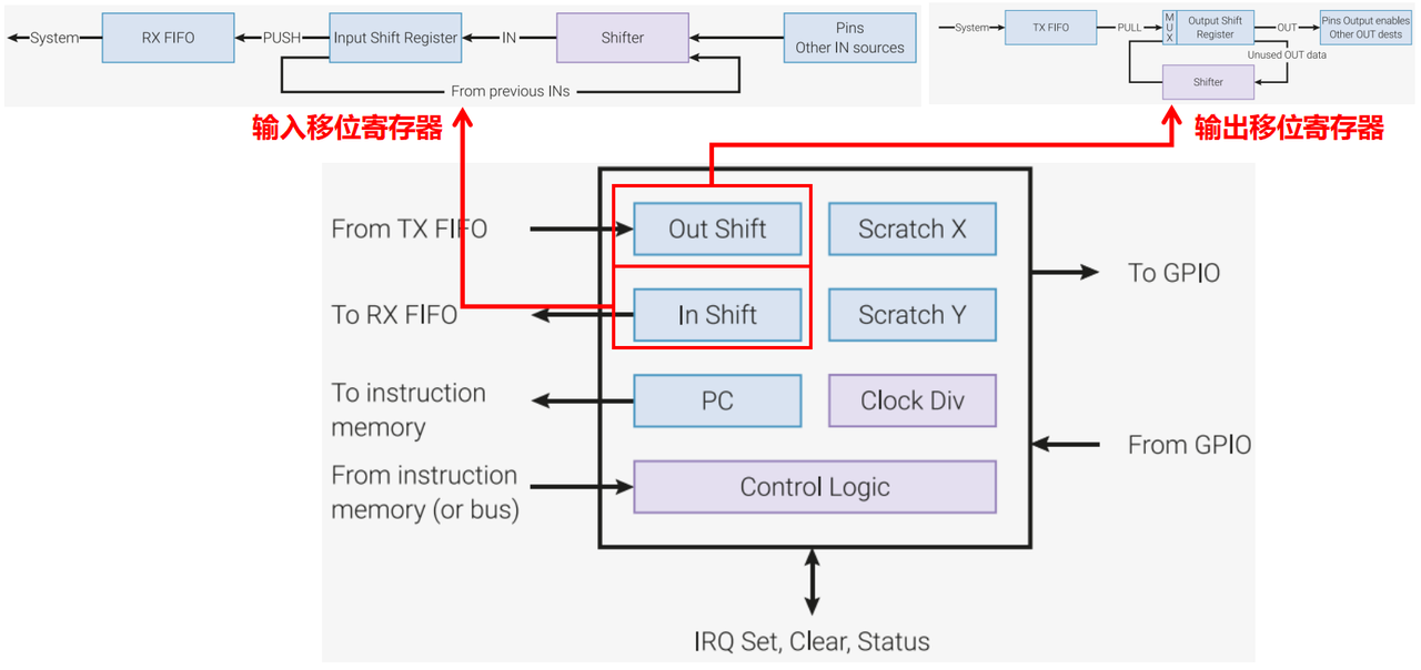
Two 32-bit shift registers: corresponding to the "Out Shift (output shift register)" and "In Shift (input shift register)" in the structure diagram, both have a width of 32 bits and support data shift operations in any direction and with any number of bits:
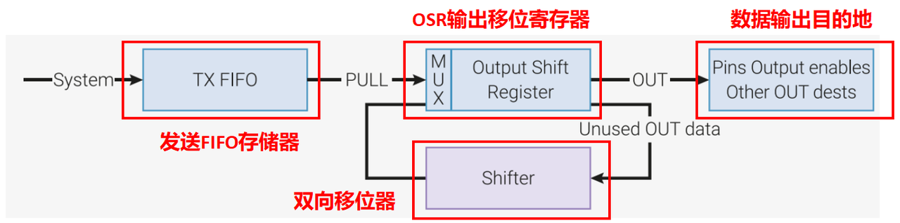
Output Shift Register (OSR): It receives data from the TX FIFO, shifts the data according to the rules configured by the instruction, and then outputs it to the GPIO.
Input Shift Register (ISR): It reads data from GPIO, shifts and temporarily stores the data according to instruction rules before writing it to the RX FIFO. The shift register serves as the core data path connecting the finite-state machine to the FIFO and GPIO.
Two 32-bit erasable registers: Corresponding to "Scratch X" and "Scratch Y" in the structure diagram, both are 32 bits wide, serving as temporary data storage units for the finite-state machine during program execution, which can be analogized to "variables" in general programming and are used to temporarily store intermediate operation results, configuration parameters, etc. ;
There are 4x32-bit bus FIFOs in each direction (TX/RX): corresponding to the "TX FIFO" and "RX FIFO" connected to the shift register in the structure diagram, which are the asynchronous data buffer units between the finite-state machine and external devices (CPU/DMA):
Hardware Specifications: Each finite-state machine is default equipped with 4×32-bit FIFO in both directions (4 pieces of 32-bit data depth for TX FIFO and RX FIFO respectively), and we can use the SHIFTCTRL_FJOIN option to merge them into an 8×32-bit unidirectional FIFO, which is suitable for high-bandwidth scenarios such as DPI image display;
Data Interaction:
TX FIFO: To be written with to-be-output data by the CPU or DMA for the finite-state machine to read from the Out Shift register;
RX FIFO: Written by the finite-state machine with data from the In Shift register for reading by the CPU or DMA.
Rate Adaptation: The FIFO can generate DREQ request signals (the communication channel between the peripheral device and the DMA), and the DMA controller can perceive the storage status of the FIFO (full / non-empty / empty, etc.) based on this signal, and dynamically adjust the transmission rhythm to achieve rate matching.
Clock Divider (Clock Div): Corresponding to the "Clock Div" in the structure diagram, it is a fractional divider with a 16-bit integer part plus an 8-bit fractional part:
The clock source is the system clock (e. g., 125MHz), which can divide the clock of the finite-state machine down to 1/65536 of the system clock (the lowest divided clock at 125MHz is approximately 1908Hz);
Its core function is to set an accurate operating rate for scenarios such as serial communication to ensure timing matching.
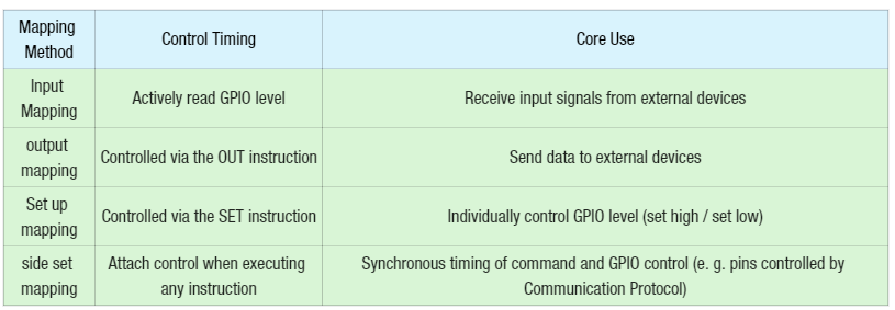
Flexible GPIO mapping: The finite-state machine supports 4 independent GPIO mapping modes (input mapping, output mapping, set mapping, and side-set mapping), and each finite-state machine can independently map its I/O operations to the GPIO pins of the RP2040 (up to 30 available GPIOs are supported), enabling flexible pin allocation;
DMA Interface: The finite-state machine is connected to the on-chip DMA controller via the DMA interface, which can achieve a maximum interaction rate of "1 byte of data transferred per system clock" and supports efficient transmission of large volumes of Big data;
Interrupt System: Corresponding to the "IRQ Set, Clear, Status" in the structure diagram, the PIO peripheral contains a total of 8 interrupt flag bits:
Interrupt sources may come from the FIFO (e. g., FIFO full/empty) or a finite-state machine (e. g., instruction execution completed);
Synchronization between finite-state machines, as well as between a finite-state machine and the main CPU, can be achieved by setting, clearing, and querying the status of interrupt flags.
Program Counter (PC): Corresponding to the "PC" module in the structure diagram, it is the instruction address pointer of the finite-state machine, used to point to the storage location of the PIO assembly instruction to be executed currently in the instruction memory, and control the sequential execution flow of instructions;
Control Logic Block: corresponds to the "Control Logic" module in the structure diagram, and serves as the control hub of the finite-state machine. The system can configure and control the working status of other components of the finite-state machine (such as shift registers, clock dividers, etc.) by reading and writing the registers in this module.
The PIO finite-state machine cannot directly execute assembly instructions written by humans; it requires the pioasm compiler (PIO Assembler) to compile dedicated assembly instructions into corresponding machine codes, which are then loaded into the PIO's instruction memory for execution by the finite-state machine. PIO provides 9 core pioasm assembly instructions that cover all relevant basic operations such as jumps, data transfer, GPIO control, and interrupt handling, serving as the core syntax for implementing PIO functions. The specific instructions and their functions are as follows:
JMP: Jump Instruction
Function: Modify the program counter (PC) value of the finite-state machine to redirect the instruction execution flow to the specified memory address, supporting both unconditional jumps and conditional jumps (e. g., determining whether to jump based on conditions such as register values, pin states, and FIFO states).
Purpose: It implements logics such as branching, looping, and conditional execution of programs, serving as the fundamental instruction for building complex PIO programs.
WAIT: Wait Instruction
Function: Pause the execution of the finite-state machine, and resume executing subsequent instructions until the preset waiting condition is satisfied. The waiting conditions are mainly divided into two categories:
First, GPIO pin status conditions (e. g., waiting for a certain GPIO pin to be at high level / low level);
Second, there is the clock cycle condition (e. g., waiting for a specified number of finite-state machine clock cycles to achieve precise delay).
Purpose: To realize timing synchronization with external devices (e. g., waiting for the ready signal of a sensor), generate precise delay operations, and ensure the timing determinacy of PIO operations.
IN: Data Read Instruction
Function: It reads data from a specified source and shifts it into the input shift register (ISR). The data sources include GPIO pins (for reading the level state of a single or multiple GPIOs), FIFO memory, internal registers of the finite-state machine, etc. , and supports specifying the number of bits to be read.
Purpose: It implements the core operation of reading data from external devices (via GPIO) or internal units, and serves as the primary method for PIO input data acquisition.
OUT: Data Write Instruction
Function: This module shifts out the data in the Output Shift Register (OSR) and writes it to the specified targets, including GPIO pins (for controlling GPIO output levels), FIFO memory, internal registers of the finite-state machine, etc. , and supports specifying the number of bits to be written.
Purpose: It implements the core operation of sending data to external devices (via GPIO) or internal units, and serves as the primary method for PIO to output data.
PUSH: Data Push Instruction
Function: This instruction pushes the complete data in the Input Shift Register (ISR) into the RX FIFO. After the push operation, you can choose to clear the ISR or retain the data, and you can also configure whether to trigger an interrupt during the push process.
Purpose: To transfer the data read by the finite-state machine from the GPIO to the CPU or DMA (via the RX FIFO), so as to complete the external interaction of PIO input data.
PULL: Data Pull Instruction
Function: Pulls data from the TX FIFO and loads it into the Output Shift Register (OSR); after the pull operation, it is configurable whether to wait for data when the TX FIFO is empty, and meanwhile, the option to clear the OSR or retain the original data is available.
Purpose: It transfers the data written by the CPU or DMA (stored in the TX FIFO) to the finite-state machine, serving as the data source for PIO output.
MOV: Data movement instruction
Function: It can move or copy data between the internal registers of the finite-state machine, with supported operation objects including the input shift register (ISR), output shift register (OSR), X/Y erasable registers, GPIO pin configuration register, etc. , and can also implement simple operations such as data inversion and zero clearing.
Purpose: To implement data processing inside the finite-state machine and data interaction between registers, which is equivalent to the variable assignment operation in general-purpose programming.
IRQ: Interrupt Write or Clear Instruction
Function: This function operates on the interrupt flag bits of PIO, including setting the interrupt flag (triggering an interrupt), clearing the interrupt flag (canceling an interrupt), and waiting for the interrupt flag (pausing execution until the interrupt is triggered); the interrupt flag bits to be operated can be specified (PIO has a total of 8 interrupt flag bits).
Purpose: It implements synchronization between finite-state machines and event notification between finite-state machines and the main CPU, serving as the core operation instruction of the PIO interrupt mechanism.
SET: Instruction for configuring mapped GPIO
Function: Directly set the level state (high level / low level) of the specified GPIO pin, or configure the mapping mode (input / output / set / side set) of the GPIO; the GPIO to be operated is the pin that has been mapped by the finite-state machine.
Purpose: It enables rapid level control over GPIO pins, and is suitable for simple output operations or GPIO mode configuration.
1. Control Flow of PIO
One of the core features of the PIO finite-state machine is the timing determinism of instruction execution, which is guaranteed by its fixed control flow mechanism. The instruction execution process of the finite-state machine follows strict clock cycle rules and supports flexible instruction fetch and execution methods, with the specific mechanism as follows.
1.1 Instruction Execution Cycle of the finite-state machine
Each PIO finite-state machine completes the three stages of fetching, decoding, and executing one pioasm assembly instruction within a single system clock cycle (these three stages are finished in one clock cycle with no pipeline latency). Only special instructions (such as the WAIT instruction, which requires waiting for the condition to be met before proceeding) will break this rule and cause the finite-state machine to pause execution.
To enable cycle-accurate programming, PIO instructions also support the insertion of delay cycles: before the next instruction is executed, users can manually configure to insert 1 to 31 additional clock cycle delays. This delay configuration is instruction-level, which can accurately match the timing requirements of external devices, such as the clock beats of serial communication and the response time of peripherals.
1.2 Working Mechanism of the Program Counter (PC)
The program counter (PC) is a core component of the finite-state machine that controls the instruction execution sequence, and its operating logic is as follows:
Default behavior: During the normal execution flow, the value of the PC is automatically incremented by 1 at each clock cycle, pointing to the address of the next instruction in the instruction memory to realize sequential instruction execution.
Exception: When executing the JMP (jump) instruction, the default auto-increment logic of the PC will be overridden;the JMP instruction explicitly specifies the next value of the PC (i. e., the position of the next instruction to be executed in the instruction memory), thereby implementing control flow logic such as program branching, looping, and conditional jumps.
1.3 Extended Acquisition Sources of Instructions
By default, the instructions executed by the finite-state machine are fetched from the PIO's instruction memory, but to enhance flexibility, the PIO also supports fetching and executing instructions from the following special regions, which enable advanced operations of "instruction and data stream fusion":
Special Configuration Register (SMx INSTR)
Mechanism: When writing an instruction to the SMx INSTR register corresponding to the finite-state machine (where x is the finite-state machine number, ranging from 0 to 3), this instruction will immediately interrupt the current instruction execution flow of the finite-state machine and be executed with priority.
Example: Write a SMx INSTR entry with the JMP instruction; the finite-state machine will immediately abandon the currently executing instruction sequence and start executing new instructions from the address specified by the JMP instruction.
Features: It has the highest execution priority and is suitable for urgent command intervention or immediate Retargeting of a finite-state machine.
MOV EXEC Instruction
Mechanism: Through MOV EXEC instruction, the finite-state machine can read and execute instructions from internal registers (instructions are stored in registers in the form of data).
Execution Timing: MOV EXEC the instruction itself requires 1 clock cycle to execute, followed by another 1 clock cycle to execute the target instruction read from the register.
OUT EXEC instruction
Mechanism: Through OUT EXEC instruction, the finite-state machine can read and execute instructions from the Output Shift Register (OSR), where the instructions are embedded as data in the data stream of the shift register.
Execution timing: consistent with MOV EXEC, the OUT EXEC instruction itself occupies 1 clock cycle, and then the target instruction is executed.
2. Introduction to internal registers of PIO finite-state machine
Each finite-state machine has several internal registers, which are used to store temporary data such as input or output data and loop variables.
Data transfer among multiple registers is realized via the control logic of a finite-state machine: for instance, the IN instruction shifts GPIO data into the In Shift, after which the data can be copied to the Scratch X for temporary storage via the MOV instruction; once processing is completed, the data is written to the Out Shift via the MOV instruction, and finally output to GPIO via the OUT instruction. The entire process requires no intervention from the main CPU, ensuring the independence, high efficiency and timing accuracy of the PIO.
2.1 Output Shift Register (OSR)
Corresponds to the Output Shift Register module in the output data flow diagram, which serves as the temporary storage and processing unit for finite-state machine output data. Its hardware connection is structured as: TX FIFO (Transmit FIFO Memory) → OSR → Bidirectional Shifter → Output Destinations (such as Pins Output enables).
It is responsible for implementing data storage and shift output between the TX FIFO and GPIO pins (or other output targets such as erasable registers), supporting a maximum of 32 bits of Data Parallelism output in a single operation; unused output data will be recovered by the bidirectional shifter to avoid data loss:
Data loading: The PULL instruction is used to pull data from the TX FIFO and store it in the OSR; when the OSR is empty, data will also be automatically loaded from the TX FIFO.
Data Output: The OUT instruction is used to output the data in the OSR to the specified target, with a single output supporting 1 to 32 bits of data; upon completion of the output, the OSR will be fully filled with 0s.
Autopull: This function can be enabled by configuring the control logic block. When the output shift counter reaches the set threshold, the finite-state machine will automatically execute PULL instruction to load data from the TX FIFO. This function eliminates the need to manually execute the PULL instruction, thus saving instruction cycles and improving data throughput.
2.2 Input Shift Register (ISR)
Corresponding to the one in the input data flow diagram Input Shift Register module, it is the temporary storage and processing unit for the input data of the finite-state machine, and its hardware connection relationship is: input source (Pins, etc.) → bidirectional shifter (Shifter) → ISR → RX FIFO (receive FIFO memory).
It is responsible for implementing data storage and shift input between GPIO pins (or other input sources) and the RX FIFO, supporting up to 32 bits of Data Parallelism input in a single operation; unprocessed input data will be temporarily stored by the bidirectional shifter to ensure data continuity:
Data input: The IN instruction is used to shift data from the bidirectional shifter into the ISR, with a single input supporting 1 to 32 bits of data.
Data Push: The data in the ISR is written to the RX FIFO via the PUSH instruction for reading by the CPU or DMA.
Auto-push (autopush): This function can be enabled by configuring the control logic block. When the input shift counter reaches the set threshold, the finite-state machine automatically executes the PUSH instruction to push the data in the ISR to the RX FIFO.
2.3 Shift Counter Shifter
It is a pair of hardware counters (input shift counter, output shift counter) built into the finite-state machine, which are used to track the number of input data bits of the ISR and the number of output data bits of the OSR, with a counting range of 0 to 32 (inclusive of the boundary values):
Each time an IN instruction is executed, the input shift counter increments by the corresponding number of data bits;
Each time an OUT instruction is executed, the output shift counter increments by the corresponding number of data bits;
The maximum value of the shift count is 32, which is consistent with the width of the shift register.
When the counter reaches the specified threshold as configured via the control logic block, the following operations will be automatically triggered:
When the output shift counter reaches the threshold: automatically execute OUT instruction to output the OSR data to the target;
When the input shift counter reaches the threshold, the IN instruction is automatically executed to shift the data of the bidirectional shifter into the ISR;
Automatic execution based on counter conditions PUSH / PULL:
Automatic PULL (between OSR and TX FIFO): The output shift counter is cleared upon execution;
Automatic PUSH (between ISR and RX FIFO): The input shift counter is cleared upon execution.
When reset (or enabling CTRL_SM_RESTART): the input shift counter is cleared (indicating no input data in the ISR), and the output shift counter is set to 32 (indicating no output data in the OSR):
MOV OSR, . ..(the MOV instruction written to OSR): clear the output shift counter;
MOV ISR, . ..(the MOV instruction written to ISR): input shift counter cleared;
OUT ISR, count: Set the input shift counter to count.
2.4 Erasable and Writable Registers
Each finite-state machine contains two independent 32-bit general-purpose registers (named X and Y) with no fixed function binding, serving as the "temporary variable carrier" for PIO programs:
As the source/target address for data operations: supports IN / OUT / SET / MOV and other instructions for data transfer;
Data source as a branch condition: supports JMP and other instructions for conditional judgment.
The following is a sample assembly program for operating the erasable register. In the code below, we generate multiple sequences of long high-level pulses and short low-level pulses to form the timing signals required for WS2812, so as to control the WS2812 LED strip:
.program ws2812_led

public entry_point:
    pull ; 用于获取输入引脚的当前状态
    set x, 23 ; 将寄存器x初始化为23,用于循环控制24个位

bitloop:
    set pins, 1 ; 将输出引脚驱动为高电平
    out y, 1 [5] ; 将输出移位寄存器的1位数据输出,并写入y寄存器中
    jmp !y skip ; 根据y寄存器的值判断是否需要执行额外的延时,若y为0则跳转到skip程序
    nop [5] ; 延时5个时钟周期

skip:
    set pins, 0 [5] ; 将输出引脚驱动为低电平
    jmp x-- bitloop ; 若x寄存器非0则递减,并根据x的值判断是否需要继续循环,非0则继续跳转到bitloop程序
    jmp entry_point ; 循环结束后,跳转回程序入口点
wherein the public entry_point: statement is used to define the program entry point, and the bitloop: statement label defines the start position of the bit loop:
The function of register X: it serves as a loop counter, whose initial value 23 corresponds to 24-bit data (the color data length of a single WS2812 LED bead), and is decremented via x-- in each loop to realize the control of 24-bit output;
The function of register Y: as a temporary variable, it stores the 1-bit data shifted out from the OSR, and is used for JMP instruction condition judgment (to distinguish different delays corresponding to 0/1 and match the timing requirements of WS2812);
The execution process of the code is as follows:
The program first acquires the current state of the input pin and pulls the LED pixel data from the TX FIFO;
Then enter the bit loop, which is controlled by X to run 24 times, and each loop outputs one bit value (0 or 1) to the LED strip;
Loop 24 times to complete the output of 24 bits, distinguish the bit values via Y and generate the corresponding timing sequence;
Finally, jump back to the program entry point and repeat the above process.
3. Wait state of the PIO finite-state machine
The instruction execution of the PIO finite-state machine generally follows a single-cycle completion rule, but under specific conditions, the finite-state machine will enter a wait state (pausing instruction execution). The wait state is a hardware behavior designed by PIO to adapt to external timing and data interaction rhythm, and its trigger conditions, hardware performance and special processing mechanisms are as follows.
3.1 Trigger Conditions for the finite-state machine to Enter the Waiting State
The core reason why the finite-state machine pauses execution is that the execution conditions of the current instruction are not met, which can be specifically divided into the following five scenarios:
The delay condition for the WAIT instruction is not met: When executing WAIT delay instruction, if the preset delay time has not yet elapsed (or the GPIO pin status or interrupt flag does not meet the waiting condition), the finite-state machine will suspend execution until the condition is satisfied;
Abnormal FIFO status of blocking PULL/PUSH instructions:
When executing the blocking modePULL instruction, if the TX FIFO is empty (no data available to be pulled), the finite-state machine will pause until the CPU/DMA writes data to the TX FIFO;
When executing the blocking mode of the PUSH instruction, if the RX FIFO is full (no space to store data), the state machine will pause until the CPU/DMA reads data from the RX FIFO;
The PULL/PUSH instructions of PIO support both blocking and non-blocking modes. The behavior described above corresponds to the blocking mode, and no waiting will be triggered in the non-blocking mode.
The interrupt flag bit of the IRQ WAIT instruction is not cleared: When executing the IRQ WAIT instruction, if the IRQ interrupt flag bit set in the instruction is not cleared (the interrupt is not released), the state machine will pause execution until the interrupt flag bit is cleared;
OUT instruction trigger wait under autopull: After the autopull function is enabled, when the OSR reaches the count threshold of the shift counter, the state machine will trigger an automatic PULL operation; if the TX FIFO is empty (no data available to load) at this time, the state machine will pause and wait for the CPU/DMA to write data to the TX FIFO.
IN instruction trigger wait under auto-push (autopush): After the autopush function is enabled, when the ISR reaches the count threshold of the shift counter, the state machine will trigger an automatic PUSH operation; if the RX FIFO is full (no space for storage) at this time, the state machine will pause and wait for the CPU/DMA to read data from the RX FIFO.
3.2 Behavior of Program Counter (PC) in Wait State
When the finite-state machine is in the waiting state, the value of the program counter (PC) remains unchanged, and no increment or jump operation will be performed. The finite-state machine rechecks the waiting condition at every clock cycle: if the condition is still not resolved, it continues to pause; if the condition is resolved, it immediately resumes executing the current instruction, and then restores the normal PC increment or instruction jump logic.
3.3 Side-set Operations and Side-set Mapping
The side-set is a combination of a special GPIO mapping method and instruction-level operations for the PIO finite-state machine. It is not only one of the four GPIO mapping modes, but also a core synchronization tool for handling wait states.
3.4 Side Set Mapping (Hardware Configuration Level)
Side-set mapping is one of the four GPIO mapping modes for PIO, whose core lies in deeply binding specific GPIOs to the instruction execution flow of the finite-state machine, and it serves as the hardware foundation for side-set operations.
Core Definition: Pre-configure the "side-set pins"(up to 5 GPIOs) for the finite-state machine, and specify the active level (high/low) of the side-set signal; when the finite-state machine executes any instruction, it can output the preset side-set signal synchronously to control the level of the corresponding pin.
Key Features: Side-set operations are completed in the same cycle as instruction execution, with no additional clock overhead, enabling extremely precise timing control.
映射方式
控制时机
核心用途
输入映射
主动读取 GPIO 电平
接收外部设备输入信号
输出映射
通过OUT指令控制
向外部设备发送数据
设置映射
通过SET指令控制
单独控制 GPIO 电平(置高 / 置低)
侧集映射
执行任意指令时附带控制
指令与 GPIO 控制的同步时序(如通信协议控制引脚)
3.5 Side Set Operation
Side set operation is an instruction-level behavior based on side set mapping, and it is the practical implementation approach of the side set function.
Number of side-set pins: Configured via PIO_SM_CONFIG 's side_set_bits field (1~5 bits, corresponding to 1~5 side-set pins);
Drive mode: Configure the active level (high/low) and drive type (push-pull/open drain) of the side set pins by means of control registers.
3.6 Special Functions of Side-set Operations
The wait state of a finite-state machine pauses most instruction-related operations, but Side-set operations are not affected by the wait state:
The side-set operation is bound to the instruction, and regardless of whether the instruction enters a waiting state, the side-set operation will be executed in the first clock cycle of the instruction it belongs to;
The core value of this feature is that even if the finite-state machine is paused, the level of the specified GPIO pin (such as the control pin of the Communication Protocol) can still be controlled through side-set operations, ensuring that the timing synchronization of external devices will not be interrupted.
The core value of side set mapping and operations lies in realizing the latency-free binding between instructions and GPIO control, which can maintain the timing stability of external devices especially in the waiting state, and typical scenarios include:
Communication Protocol Synchronization: In SPI communication, configure the chip select (CS) pin as a side-set pin, and pull CS low synchronously when OUT transmitting data; even if the pull instruction waits due to an empty TX FIFO, CS remains asserted to prevent communication abnormalities of the slave device.
High-speed Timing Generation: In the DPI display driver, set the horizontal synchronization (HSYNC) pin as a side-set pin, and execute it synchronously with the data output instruction to ensure precise timing matching between the synchronization signal and the data;
State Retention in the Waiting State: When the finite-state machine is waiting due to an interrupt, it outputs a "busy" signal via the side-set pins to prevent external devices from sending repeated requests.
4. GPIO Pin Mapping of PIO
The GPIO pin mapping of PIO is a physical connection configuration mechanism for it to interact with external hardware, which defines the rules for the finite-state machine to control and read GPIO pins, serves as the foundation for PIO to implement external interface functions, and its core logic is as follows:
GPIO Control Capabilities of PIO: PIO supports the output level and direction control for up to 32 GPIOs, as well as input level reading; in the RP2040 hardware, the actual number of user GPIOs that can be mapped is 30;
GPIO operation limit per clock cycle: Within a single system clock cycle, each finite-state machine can perform a maximum of 2 GPIO operations, and the supported operation combinations include:
Instruction-based operations: modify the level/direction of GPIO via OUT / SET instructions, or read the GPIO level via IN instruction;
Side-set Operations: Modify the GPIO level/direction via side-set operations;
Each cycle can perform "zero operations, one operation (either an instruction or a side set), or two operations (instruction + side set)".
The operation range of the finite-state machine for GPIO is determined by its PINCTRL register:
Each operation (OUT / SET / IN /side-set) can specify a consecutive block of 4 GPIOs, and the starting pin number of this GPIO block is configured via the PINCTRL register;
The GPIO coverage of a single operation can be extended to any number of GPIOs within the PIO block (30 user GPIOs in the RP2040);
GPIO ranges for different operations (such as OUT and side-set) can overlap, allowing the same GPIO group to be controlled by multiple operations.
When multiple operations write to the same GPIO in the same clock cycle, the PIO applies the operation results according to the following priority rules:
finite-state machine priority: starting from the finite-state machine with the largest number, apply its write operations in sequence;
Operation priority for the same finite-state machine: When the same finite-state machine performs SET / OUT and side-set operations on the same GPIO simultaneously, the result of the side-set operation takes effect first;
Retention rule for no write operation: If no finite-state machine performs a write operation on a certain GPIO, the level/direction of this GPIO will maintain the state of the previous cycle.
In practical applications, the output operations of each finite-state machine are usually mapped to different GPIO groups, so that a single PIO block can drive multiple independent external interfaces simultaneously (for example, one finite-state machine maps GPIO0~3 to implement UART, and another finite-state machine maps GPIO4~7 to implement SPI), thus maximizing the utilization of PIO hardware resources.
5. IRQ Interrupt Flag Bit of PIO
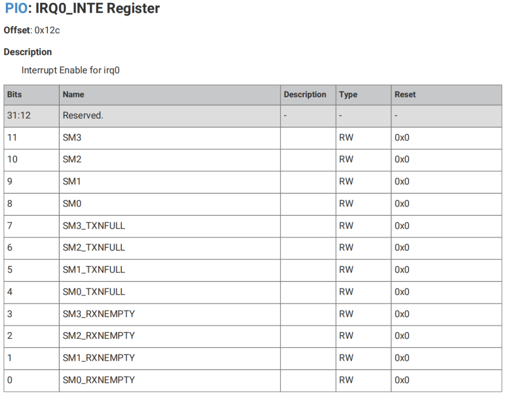
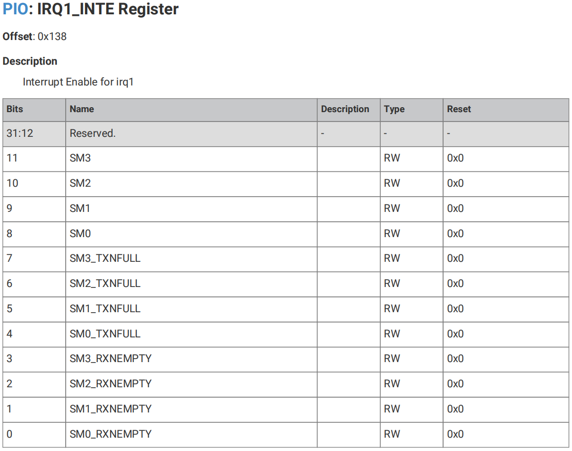
The IRQ interrupt mechanism of PIO implements synchronization between finite-state machines and communication between finite-state machines and the main CPU, serving as the core approach, which consists essentially of the "IRQ interrupt flag bits" and the "interrupt enable registers (IRQ0_INTE, IRQ1_INTE)".
The IRQ interrupt flag bits of PIO are status bits that can be set/cleared by a finite-state machine or the system, which are used to indicate the occurrence of specific events. There are 12 flag bits in total (corresponding to the register bit definitions), and they are divided into three categories:
SMx flag bits (x= 0~3): System-level interrupt flag bits, which are actively set by a finite-state machine or the system, and are used for synchronization between finite-state machines or triggering interrupts of the main CPU;
SMx_TXNFULL flag bits (x= 0~3): These are the TX FIFO non-full flag bits of finite-state machine x, which are triggered when there is free space in the TX FIFO;
SMx_RXNEMPTY flag (x= 0~3): This is the RX FIFO non-empty flag for finite-state machine x, which is triggered when there is data in the RX FIFO.
The status of these flags can be read from the PIO's INTR (Interrupt Status Register) and INTS (Interrupt Original Status Register).
IRQ0_INTE and IRQ1_INTE are the interrupt enable configuration registers of PIO, which are used to control which IRQ flags can trigger interrupt requests (corresponding to the irq0 and irq1 interrupt lines of RP2040), and the two structures are completely consistent, only corresponding to different interrupt lines.
IRQ0_INTE IRQ1_INTE The low 12 bits of the register (Bit0~ Bit11) correspond to various IRQ interrupt flags of PIO (including 4 system-level SMx flags, 4 TX FIFO non-full flags, and 4 RX FIFO non-empty flags), and the high bits (Bit12~ Bit31) are reserved bits reserved by the chip (no function, no need to worry):
Enable configuration : write 1 to the corresponding bit of the register, indicating that the enable flag triggers the corresponding irq (irq0 or irq1); write 0 to mask the interrupt request of the flag;
Reset status : The reset value of all bits in the register is 0x0 , that is, after PIO initialization, the interrupts of all IRQ flags are in the masked state by default;
Interrupt triggering : When a flag is set and the corresponding enable bit is 1 , PIO will send an irq0/irq1 request to the interrupt controller of RP2040, triggering the interrupt processing flow of the main CPU.
IRQ flags are mainly used for the following purposes:
Event handling within a finite-state machine program: A finite-state machine can implement conditional execution logic within the program via IRQ instructions (for setting/clearing flag bits) and WAIT instructions (for waiting for flag bit states);
Synchronization between finite-state machines: Multiple finite-state machines can synchronize their execution timings by sharing IRQ flags (for example, finite-state machine A sets a flag after completing an operation, and finite-state machine B starts running after waiting for this flag to be set);
Communication with the main CPU: By enabling the interrupt of the flag bit, the finite-state machine can notify the main CPU of events (such as TX FIFO being empty and RX FIFO having data) to trigger subsequent processing of the CPU.
6. Synchronization of PIO finite-state machine
The 4 finite-state machines of the PIO feature parallel execution and independent operation, and support precise clock-cycle-level synchronization via IRQ interrupt flags, which is the core capability that enables the PIO to handle multiple interfaces or complex timing tasks simultaneously. The 4 finite-state machines of the PIO share the instruction memory but operate in full parallel at the execution level, multiple finite-state machines can read and execute the same instruction (or different instructions) from the instruction memory within the same system clock cycle without waiting for each other:
Multiple finite-state machines execute the same program:
Scenario: It is required to drive multiple identical external devices at the same time (such as multiple sets of WS2812 LED strips, multiple identical SPI slave devices).
Advantages: Only need to write a PIO assembly program, multiple fine-state machines can execute in parallel, reducing the workload of program development and ensuring the consistency of device control logic.
Multiple fine-state machines execute different programs.
Scenario: Multiple different Communication Protocols or I/O functions need to be implemented simultaneously (such as one fine-state machine implementing UART transmission, one implementing SPI reception, and one implementing GPIO pulse detection).
Advantages: A single PIO block can handle multiple independent I/O tasks simultaneously, maximizing the use of PIO hardware resources and avoiding occupying the computing power of the main CPU.
Multiple fine-state machines execute different units of the same interface.
Scenario: Functional splitting of complex interfaces, assigning different timing tasks to different fine-state machines.
Example:
UART communication: One fine-state machine is responsible for the TX (sending) end, and the other is responsible for the RX (receiving) end.
DPI image display: one fine-state machine is responsible for clock/horizontal synchronization signal generation, and the other is responsible for pixel data output.
Advantage: Split complex timing into simple subtasks, reduce the difficulty of writing a single program, and ensure the timing synchronization of each unit of the interface.
PIO's fine-state machines cannot directly communicate with each other, but precise synchronization can be achieved through the IRQ interrupt flag, and the synchronization accuracy can reach a single clock cycle. The specific implementation method is as follows:
Core Tool for Synchronization: The 8 IRQ interrupt flags of PIO (system-level SMx flags, FIFO status flags) serve as the "synchronization signal carriers" between finite-state machines, and all finite-state machines can read, set, and clear these flags.
Synchronous instruction support:
IRQ instruction: Any finite-state machine can use this instruction to set or clear any IRQ flag bit (for example, after finite-state machine 0 completes data transmission, the SM0 flag bit is set);
WAIT IRQ Instruction: The finite-state machine can use this instruction to wait for a certain IRQ flag bit to be set or cleared (for example, finite-state machine 1 waits for the SM0 flag bit to be set before starting data reception).
Synchronous implementation logic: Through the process of "finite-state machine A sets/clears the flag bit → finite-state machine B waits for the flag bit state to change before executing operations", the execution rhythm alignment of multiple finite-state machines is realized, achieving clock cycle-level synchronization effect.