RP2040 PIO Instruction Set Deep‑Dive: Starting from the Datasheet
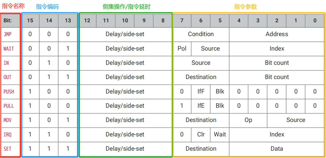
RP2040 PIO‑instructions are 16‑bit wide, split into 3 fields: 3‑bit opcode, 5‑bit side‑set/delay, and 8‑bit parameter.
COMPONENTS
PROJECT DESCRIPTION
【Preliminary Note】The original hardware example in this article was written based on the RP2040. The actual hardware used in this hands-on demonstration features the W55RP20 as the main controller chip. The circuit logic and UF2 flashing operation principles are universally applicable, with only the main controller model differing. The original chip model mentioned in the circuit descriptions below is provided for reference purposes only.
Tweet:
PIO Instruction Set
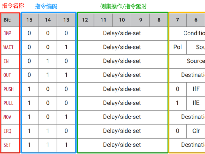
The PIO instruction set contains a total of 9 instructions, each of which is 16 bits in length, and is divided into 3 fixed fields according to functions (corresponding to the instruction encoding table):
Instruction Encoding Field (Bit15~13): 3 bits, used to distinguish different instructions (e. g., JMP corresponds to 000, WAIT corresponds to 001);
Side Set / Delay Period (Bits 12~8): 5 bits, used to store the side set operation value and the number of delay cycles; the specific allocation rule depends on the SIDESET_COUNT configuration of the finite-state machine (up to 5 bits, where SIDESET_COUNT bits are allocated for the side set, and the remaining bits are used for delay);
Instruction Parameter Field (Bit 7 to Bit 0): 8 bits, used to store specific parameters of the instruction such as conditions, addresses, source/destination, and bit length.
All PIO instructions have an execution time of one clock cycle.
The meaning of the 5-bit long Delay/side-set field depends on the SIDESET_COUNT configuration of the finite-state machine:
Up to 5 LSB bits (with a bit length of 5 - SIDESET_COUNT) represent the number of Delay cycles inserted between the current instruction and the next instruction
Up to 5 MSB bits (with a bit length of SIDESET_COUNT) are used for side-set operations, which can set certain GPIO pins to a specific constant while the instruction is being executed
Here, the delay operation can be applied when we require precise timing and/or signal synchronization, while the side-set operation allows us to additionally set pins while executing an instruction. This is very useful for control signals such as clock and enable: the side-set operation is used to control pins, while instructions like OUT and MOV are used to process data.
The specific meaning of each instruction is introduced as follows.
1. JMP Jump Instruction
The JMP jump instruction is used to determine whether to perform an instruction jump according to a condition, so as to change the sequential execution flow of the current program.
According to Condition, judge whether to modify the program counter (PC): if the condition is true, set the PC to the instruction address corresponding to Address; otherwise, keep the PC incrementing. Regardless of whether the condition is satisfied, the instruction consumes 1 clock cycle, and the delay is executed after the condition evaluation.
When the JMP instruction is executed, it always consumes one clock cycle regardless of whether the Condition is true. The Delay occurs after the Condition is evaluated and the program counter is updated.
The parameters are defined as follows:
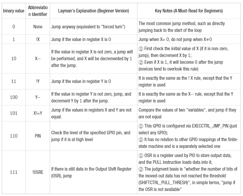
Condition: Condition is a 3-bit binary value (ranging from 000 to 111) that determines "when the jump occurs". You can think of it as a "switch for whether to jump", and each switch corresponds to a different judgment rule;
Address: Address is a 5-bit binary value corresponding to an integer ranging from 0 to 31, which represents the absolute address of the target instruction in the PIO instruction memory (can be understood as the "instruction number").
Condition The values and their corresponding meanings are as follows:
binary value
Abbreviation Identifier
Layman's Explanation (Beginner Version)
Key Notes (A Must-Read for Beginners)
0
None
Jump anyway (equivalent to "forced turn")
The most common jump method, such as directly jumping back to the start of the loop
1
!X
Jump if the value in register X is 0
Jump when X= 0, do not jump when X≠0
10
X--
If the value in register X is not zero, a jump will be performed, and X will be decremented by 1 after the jump.
① First check the initial value of X (if it is non-zero, jump), then decrement X by 1; ② Even if X is 1, it will become 0 after the jump (novices tend to overlook this rule)
11
!Y
Jump if the value in register Y is 0
It is exactly the same as the ! X rule, except that the Y register is used
100
Y--
If the value in register Y is not zero, jump, and decrement Y by 1 after the jump.
It is exactly the same as the X-- rule, except that the Y register is used
101
X!=Y
Jump if the values in registers X and Y are not equal.
Compare the values of two "variables", and jump if they are not equal
110
PIN
Check the level of the specified GPIO pin, and jump if it is at high level
① This GPIO is configured via EXECCTRL_JMP_PIN (just select any GPIO); ② It has no relation to other GPIO mappings of the finite-state machine and is a separately selected one
111
!OSRE
If there is still data in the Output Shift Register (OSR), jump
① OSR is a register used by PIO to store output data, and the PULL instruction loads data into it; ② The judgment basis is "whether the number of bits of the moved-out data has not reached the threshold (SHIFTCTRL_PULL_THRESH)", in simple terms, "jump if the OSR is not available"
Address The values and their corresponding meanings are as follows:
The instruction memory of PIO can store up to 32 instructions, so the addresses can only range from 0 (the first instruction) to 31 (the last instruction);
You don't need to calculate this address manually; just use a label (such as loop) as a substitute when writing the program, and the SDK will automatically convert the label to an absolute address. Beginners don't need to concern themselves with the conversion process — just remember to use labels.
The assembly syntax is as follows: jmp (<cond>) <target>
Wherein:
<cond> is the optional condition listed in the previous section. If no condition is specified, the jump will always be executed.
<target> is a program label or value that represents the instruction offset inside the program (the offset of the first instruction is 0).
Note that since the PIO JMP instruction uses an absolute address within the PIO instruction memory, the JMP needs to be adjusted at runtime according to the program's loading offset.
This step is handled by the SDK when loading the program, but this point needs to be noted when encoding JMP instructions for use by OUT EXEC.
2. WAIT Delay Instruction
The WAIT delay instruction is used to wait for various events, such as pin state changes or interrupt occurrences.
The WAIT delay instruction keeps waiting for the event specified by Source to meet the Pol polarity condition; the finite-state machine pauses execution until the condition is satisfied, and the Delay is executed after the waiting is completed.
The parameters are defined as follows:
Polarity: Polarity is a 1-bit binary value (either 0 or 1 only) that defines what state the awaited event must be in to satisfy the condition, which can be interpreted as "whether we are waiting for a 0 or a 1".
Source: Source is a 2-bit binary value (ranging from 00 to 11) that determines "what type of event we need to wait for", and it is the core selection parameter of the WAIT instruction.
Index: Index is a 5-bit binary value corresponding to an integer ranging from 0 to 31, indicating "which specific object to wait for among the selected event types".
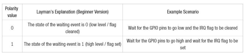
Polarity The optional values are as follows:
Polarity value
Layman's Explanation (Beginner Version)
Example Scenario
0
The state of the waiting event is 0 (low level / flag cleared)
Wait for the GPIO pins to go low and the IRQ flag to be cleared
1
The state of the waiting event is 1 (high level / flag set)
Wait for the GPIO pins to go high and wait for the IRQ flag to be set
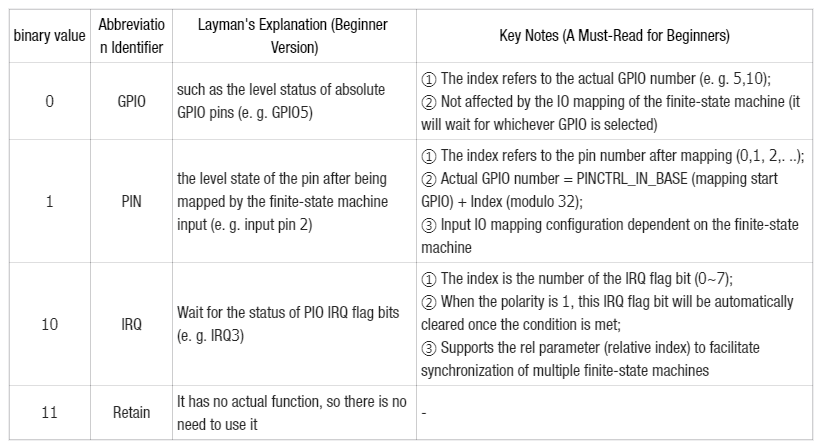
Source The optional values are as follows:
binary value
Abbreviation Identifier
Layman's Explanation (Beginner Version)
Key Notes (A Must-Read for Beginners)
0
GPIO
such as the level status of absolute GPIO pins (e. g. GPIO5)
① The index refers to the actual GPIO number (e. g. 5,10); ② Not affected by the IO mapping of the finite-state machine (it will wait for whichever GPIO is selected)
1
PIN
the level state of the pin after being mapped by the finite-state machine input (e. g. input pin 2)
① The index refers to the pin number after mapping (0,1, 2,. ..); ② Actual GPIO number = PINCTRL_IN_BASE (mapping start GPIO) + Index (modulo 32); ③ Input IO mapping configuration dependent on the finite-state machine
10
IRQ
Wait for the status of PIO IRQ flag bits (e. g. IRQ3)
① The index is the number of the IRQ flag bit (0~7); ② When the polarity is 1, this IRQ flag bit will be automatically cleared once the condition is met; ③ Supports the rel parameter (relative index) to facilitate synchronization of multiple finite-state machines
11
Retain
It has no actual function, so there is no need to use it
-
Index The optional values are as follows:
Source Type
The Meaning of Index
Value Range (Commonly Used for Beginners)
GPIO
Actual GPIO pin numbers (e. g., 0,5, 10)
0~29 (User GPIO of RP2040)
PIN
Pin numbers after finite-state machine input mapping (e. g. 0,1, 2)
0~3 (commonly used by beginners, corresponding to 4 mapping pins)
IRQ
The number of the IRQ flag bit (e. g. 0,3, 7)
0~7 (the PIO has only 8 IRQ flag bits)
The assembly syntax is as follows:
wait <polarity> gpio <gpio_num>
wait <polarity> pin <pin_num>
wait <polarity> irq <irq_num> (rel)
Wherein:
<polarity> is a value that specifies the polarity (0 or 1);
<pin_num> is a value that specifies the number of the input pin (the number in the input pin mapping of the finite-state machine);
<gpio_num> is a value that specifies the actual GPIO pin number;
<irq_num>(rel) is a value that specifies the IRQ number (0 to 7) to wait for. If rel is set, the actual IRQ number is calculated by replacing the two least significant bits of the IRQ number (irq_num (10)) with the two least significant bits of the sum (irq_num (10) + sm_num (10)), where sm_num (10) is the finite-state machine number;
3. IN Data Read Instruction
The IN data read instruction is used to transfer data from data input sources such as pin inputs or X or Y scratch registers into the ISR.
Shift SourceBit count data bits (up to 32 in maximum) into the input shift register (ISR). The shift direction is determined by the SHIFTCTRL_IN_SHIFTDIR of each finite-state machine.
The parameters are defined as follows:
Source:: the source address from which data is extracted; Source is a 3-bit binary value corresponding to different data sources;
Bit count: Bit count is a 5-bit binary value, which corresponds to the number of bits to be fetched from the data source, and the rule is very simple:
Value range: 1~32 bits (e. g., 1 bit, 8 bits, 32 bits);
Special encoding: The binary corresponding to 32 bits is 00000 (since 5 bits can represent a maximum of 31,0 is used to represent 32).
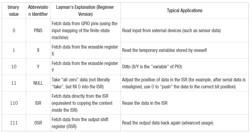
Source The optional values are as follows:
binary value
Abbreviation Identifier
Layman's Explanation (Beginner Version)
Typical Applications
0
PINS
Fetch data from GPIO pins (using the input mapping of the finite-state machine)
Read input from external devices (such as sensor data)
1
X
Fetch data from the erasable register X
Read the temporary variables stored by oneself
10
Y
Fetch data from the erasable register Y
Ditto (X/Y is the "variable" of PIO)
11
NULL
Take "all-zero" data (not literally "take", but fill 0 into the ISR)
Adjust the position of data in the ISR (for example, after serial data is misaligned, use 0 to "push" the data to the correct bit position)
110
ISR
Fetch data directly from the ISR (equivalent to copying the content inside the ISR)
Reuse the data in the ISR
111
OSR
Fetch data from the output shift register (OSR)
Read the output data back again (advanced usage)
If auto-push (autopush) is enabled, you can regard autopush as the "auto-save" function of ISR:
First, set a "persistence threshold" for the ISR (SHIFTCTRL_PUSH_THRES, e. g., 8 bits);
Each time an IN instruction is executed, the number of data bits in the ISR accumulates, and when the threshold is reached, the ISR automatically "pushes" the data to the RX FIFO (for CPU/DMA to read);
After the push operation is completed, the ISR will be cleared to 0, and data reception will be suspended simultaneously (until there is free space in the FIFO);
If the FIFO is full, the finite-state machine will "wait"(suspend execution) until there is free space in the FIFO.
IN always uses the lowest Bit count data bits of the source data. For example, if PINCTRL_IN_BASE is set to 5 (the finite-state machine input mapping starts at GPIO5), then the instruction IN 3, PINS will read pins 5,6 and 7 (not the highest bits), and shift these values into the ISR; first, the ISR will shift left or right to make space for the new input data, then copy the input data into the vacated space. It should be noted that the bit order of the input data is independent of the shift direction.
The assembly syntax is as follows: in <source>, <bit_count>
Wherein:
<source> is one of the aforementioned sources;
<bit_count> is a value that specifies the number of bits of data to be shifted (valid values range from 1 to 32).
4. OUT Data Write Command
The OUT data write instruction is used to shift data bits from the OSR to a data destination, such as a pin input or the X or Y scratch register.
Shift Bit count data bits out of the input shift register (OSR) and write them to Destination. In addition, the output shift counter Bit count will be incremented until it reaches the maximum value of 32.
The parameters are defined as follows:
Destination: the destination address where data is written. Destination is a 3-bit binary value (000 to 111), which determines the final destination of the data.
Bit count: Bit count is a 5-bit binary value, and its rules are completely identical to those of the IN instruction:
Value range: 1 to 32 bits (e. g., shift out 1 bit, 8 bits, 32 bits).
Special encoding: The binary corresponding to 32 is 00000 (since 5 bits can represent a maximum of 31,0 is used to denote 32).
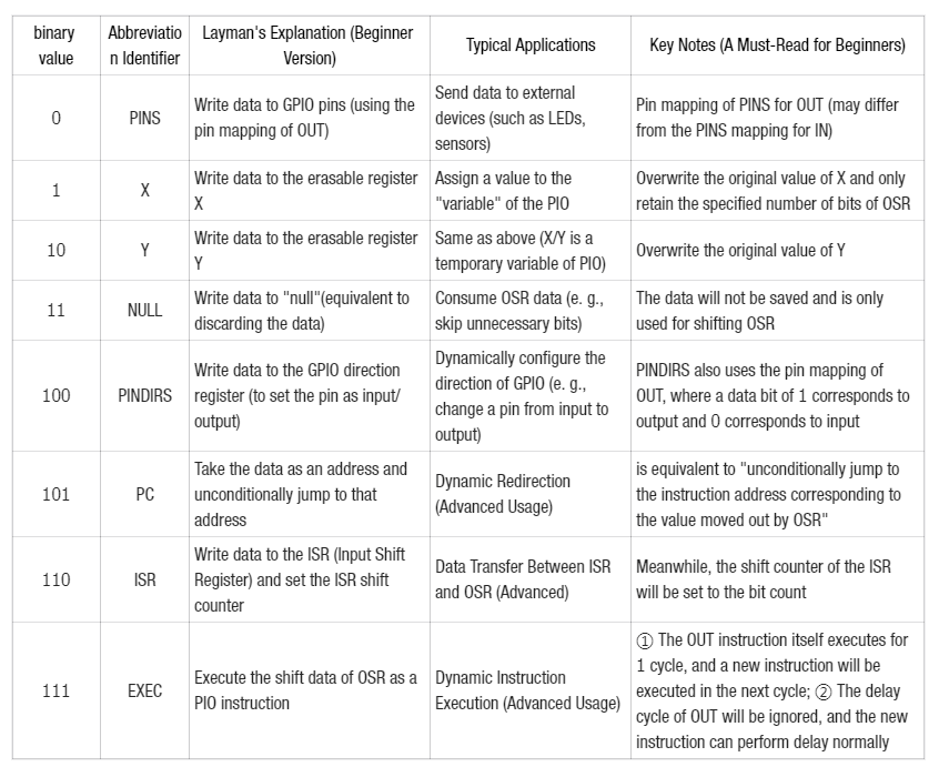
Destination The optional values are as follows:
binary value
Abbreviation Identifier
Layman's Explanation (Beginner Version)
Typical Applications
Key Notes (A Must-Read for Beginners)
0
PINS
Write data to GPIO pins (using the pin mapping of OUT)
Send data to external devices (such as LEDs, sensors)
Pin mapping of PINS for OUT (may differ from the PINS mapping for IN)
1
X
Write data to the erasable register X
Assign a value to the "variable" of the PIO
Overwrite the original value of X and only retain the specified number of bits of OSR
10
Y
Write data to the erasable register Y
Same as above (X/Y is a temporary variable of PIO)
Overwrite the original value of Y
11
NULL
Write data to "null"(equivalent to discarding the data)
Consume OSR data (e. g., skip unnecessary bits)
The data will not be saved and is only used for shifting OSR
100
PINDIRS
Write data to the GPIO direction register (to set the pin as input/output)
Dynamically configure the direction of GPIO (e. g., change a pin from input to output)
PINDIRS also uses the pin mapping of OUT, where a data bit of 1 corresponds to output and 0 corresponds to input
101
PC
Take the data as an address and unconditionally jump to that address
Dynamic Redirection (Advanced Usage)
is equivalent to "unconditionally jump to the instruction address corresponding to the value moved out by OSR"
110
ISR
Write data to the ISR (Input Shift Register) and set the ISR shift counter
Data Transfer Between ISR and OSR (Advanced)
Meanwhile, the shift counter of the ISR will be set to the bit count
111
EXEC
Execute the shift data of OSR as a PIO instruction
Dynamic Instruction Execution (Advanced Usage)
① The OUT instruction itself executes for 1 cycle, and a new instruction will be executed in the next cycle; ② The delay cycle of OUT will be ignored, and the new instruction can perform delay normally
Write a 32-bit value to Destination: the 32-bit value to be written to the destination; by default, the lower Bit count bits of OSR are taken, the upper Bit count bits are taken when shifting right, and the remaining bits are 0
If auto-loading (autopull) is enabled, autopull can be understood as the "automatic replenishment" function of OSR, which forms a pair of complementary mechanisms with the autopush of the IN instruction:
Set the threshold: First, set a "replenishment threshold" for OSR (SHIFTCTRL_PULL_THRESH, e. g., 8 bits).
Automatic replenishment: Each time an OUT instruction is executed, the output shift counter increments. When the threshold is reached, the OSR automatically loads new 32-bit data from the TX FIFO (the buffer where the CPU/DMA sends data to the PIO), and the output shift counter is cleared at the same time.
Wait mechanism: If the TX FIFO is empty (no data to fill), the state machine will suspend execution (until there is data in the TX FIFO), but the execution time of the OUT instruction remains 1 clock cycle.
The assembly syntax is as follows: out <destination>, <bit_count>
Wherein:
<destination> is one of the aforementioned data destinations
<bit_count> is a value that specifies the number of bits to be shifted (valid values range from 1 to 32)
5. PUSH Data Push Instruction
The PUSH data push instruction is used to push the 32-bit data of the ISR into the RX FIFO, and meanwhile clear the ISR, with a fixed execution time of 1 clock cycle.
Push the content of the ISR into the RX FIFO as a 32-bit word, and clear the ISR to all zeros at the same time.
The parameters are defined as follows:
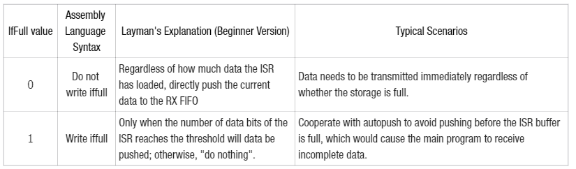
IfFull: IfFull is a 1-bit binary value (0 or 1) that determines whether to wait until the number of data bits in the ISR reaches the threshold (SHIFTCTRL_PUSH_THRESH) before pushing data;
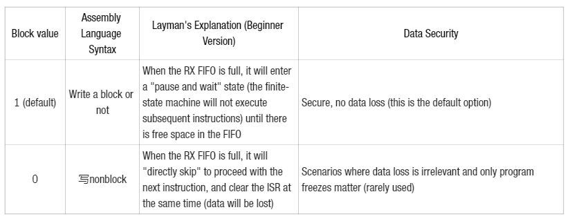
Block: Block is a 1-bit binary value (0 or 1) that determines whether to pause and wait or directly discard data when the RX FIFO is full.
IfFull has the following meaning and parameters:
IfFull value
Assembly Language Syntax
Layman's Explanation (Beginner Version)
Typical Scenarios
0
Do not write iffull
Regardless of how much data the ISR has loaded, directly push the current data to the RX FIFO
Data needs to be transmitted immediately regardless of whether the storage is full.
1
Write iffull
Only when the number of data bits of the ISR reaches the threshold will data be pushed; otherwise, "do nothing".
Cooperate with autopush to avoid pushing before the ISR buffer is full, which would cause the main program to receive incomplete data.
Block is defined with the following meanings and parameters:
Block value
Assembly Language Syntax
Layman's Explanation (Beginner Version)
Data Security
1 (default)
Write a block or not
When the RX FIFO is full, it will enter a "pause and wait" state (the finite-state machine will not execute subsequent instructions) until there is free space in the FIFO
Secure, no data loss (this is the default option)
0
写nonblock
When the RX FIFO is full, it will "directly skip" to proceed with the next instruction, and clear the ISR at the same time (data will be lost)
Scenarios where data loss is irrelevant and only program freezes matter (rarely used)
The assembly syntax is as follows:
push (iffull)
push (iffull) block
push (iffull) nonblock
Wherein:
iffull is equivalent to the aforementioned IfFull == 1, which means that if not specified, the default value is IfFull == 0;
block is equivalent to the aforementioned Block == 1; if neither block nor noblock is specified, this value is the default.
noblock is equivalent to the aforementioned Block == 0.
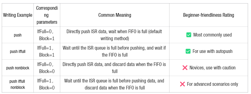
Writing Example
Corresponding parameters
Common Meaning
Beginner-friendliness Rating
push
IfFull=0,Block=1
Directly push ISR data, wait when FIFO is full (default writing method)
✅ Most commonly used
push iffull
IfFull=1,Block=1
Wait until the ISR queue is full before pushing, and wait if the FIFO is full
✅ For use with autopush
push nonblock
IfFull=0,Block=0
Directly push ISR data, and discard data when the FIFO is full
❌ Novices, use with caution
push iffull nonblock
IfFull=1,Block=0
Wait until the ISR queue is full before pushing data, and discard data when the FIFO is full
❌ For advanced scenarios only
6. PULL Data Loading Instruction
The PULL data load instruction is used to fetch one 32-bit data from the TX FIFO, load it into the OSR, and clear the OSR at the same time, with a fixed execution time of 1 clock cycle.
Load a 32-bit word from the TX FIFO into the OSR.
The parameters are defined as follows:
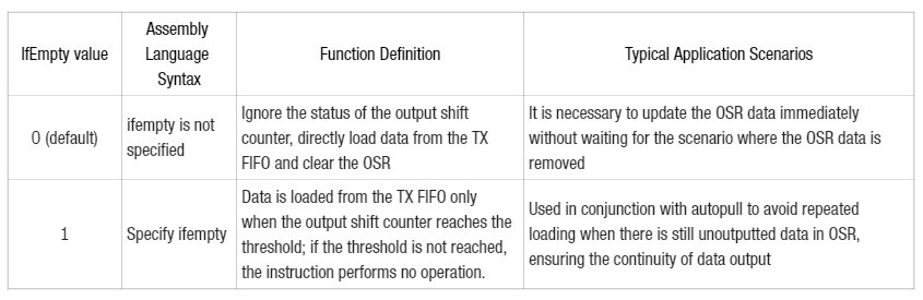
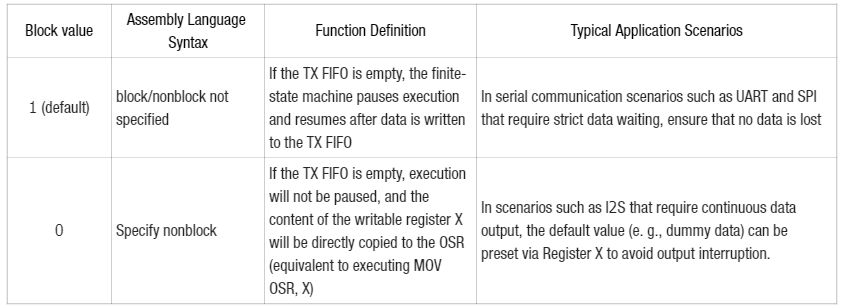
IfEmpty: IfEmpty is used to control the execution timing of the PULL instruction, and the data loading operation is performed only when the output shift counter reaches the configured threshold (SHIFTCTRL_PULL_THRESH, which is consistent with the threshold of auto-loading autopull);
Block: Block is used to define the behavior of the finite-state machine when the TX FIFO is empty, and determines whether to suspend execution to wait for data.
IfEmpty has the following meaning and parameters:
IfEmpty value
Assembly Language Syntax
Function Definition
Typical Application Scenarios
0 (default)
ifempty is not specified
Ignore the status of the output shift counter, directly load data from the TX FIFO and clear the OSR
It is necessary to update the OSR data immediately without waiting for the scenario where the OSR data is removed
1
Specify ifempty
Data is loaded from the TX FIFO only when the output shift counter reaches the threshold; if the threshold is not reached, the instruction performs no operation.
Used in conjunction with autopull to avoid repeated loading when there is still unoutputted data in OSR, ensuring the continuity of data output
Block is defined with the following meanings and parameters:
Block value
Assembly Language Syntax
Function Definition
Typical Application Scenarios
1 (default)
block/nonblock not specified
If the TX FIFO is empty, the finite-state machine pauses execution and resumes after data is written to the TX FIFO
In serial communication scenarios such as UART and SPI that require strict data waiting, ensure that no data is lost
0
Specify nonblock
If the TX FIFO is empty, execution will not be paused, and the content of the writable register X will be directly copied to the OSR (equivalent to executing MOV OSR, X)
In scenarios such as I2S that require continuous data output, the default value (e. g., dummy data) can be preset via Register X to avoid output interruption.
Note that when auto-loading is enabled, any PULL instruction is an erroneous operation when the OSR is full (i. e., the OSR still stores complete 32-bit data that has not been moved out by the OUT instruction), which will directly overwrite the new data of the TX FIFO into the OSR, resulting in the loss of the original unoutput data in the OSR. This kind of operation is an erroneous operation at the hardware level, which will damage the continuity and integrity of data output.
The "barrier" feature of the PULL instruction essentially leverages the controllability of its execution timing (via the ifempty parameter) to prevent misoperations:
When pull ifempty is configured, the PULL instruction will only be executed when the output shift counter reaches the threshold (most of the data in the OSR has been shifted out and it is nearly empty);
This is equivalent to establishing a "barrier" between the "full" and "empty" states of the OSR, ensuring that the manual PULL operation is only triggered after the OSR data has been fully output, thus preventing erroneous loading when the OSR is full.
The assembly syntax is as follows:
pull (ifempty)
pull (ifempty) block
pull (ifempty) noblock
Wherein:
ifempty is equivalent to the aforementioned IfEmpty == 1, meaning that if not specified, the default value is IfEmpty == 0
block is equivalent to the aforementioned Block == 1. If neither block nor noblock is specified, this value will be used as the default
noblock is equivalent to the aforementioned Block == 0
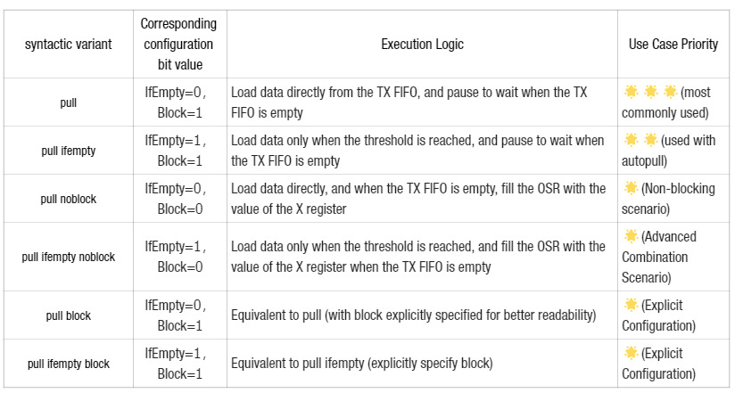
syntactic variant
Corresponding configuration bit value
Execution Logic
Use Case Priority
pull
IfEmpty=0,Block=1
Load data directly from the TX FIFO, and pause to wait when the TX FIFO is empty
🌟🌟🌟(most commonly used)
pull ifempty
IfEmpty=1,Block=1
Load data only when the threshold is reached, and pause to wait when the TX FIFO is empty
🌟🌟(used with autopull)
pull noblock
IfEmpty=0,Block=0
Load data directly, and when the TX FIFO is empty, fill the OSR with the value of the X register
🌟(Non-blocking scenario)
pull ifempty noblock
IfEmpty=1,Block=0
Load data only when the threshold is reached, and fill the OSR with the value of the X register when the TX FIFO is empty
🌟(Advanced Combination Scenario)
pull block
IfEmpty=0,Block=1
Equivalent to pull (with block explicitly specified for better readability)
🌟(Explicit Configuration)
pull ifempty block
IfEmpty=1,Block=1
Equivalent to pull ifempty (explicitly specify block)
🌟(Explicit Configuration)
7. MOV Data Movement Instruction
The MOV data transfer instruction is used to move data from a source address to a destination address. Registers and pins can be used as the source address and destination address for data transfer, as well as several locations with special functions.
Copy data from Source to Destination.
The parameters are defined as follows:
Destination : Destination is a 3-bit configuration bit that specifies the hardware unit to which the data is ultimately written, and some destinations feature special functions;
Operation: Operation is a 2-bit configuration bit, which is used to preprocess the source data before copying it;
Source: Source is a 3-bit configuration bit that specifies the source of data, in which STATUS is a special status source.
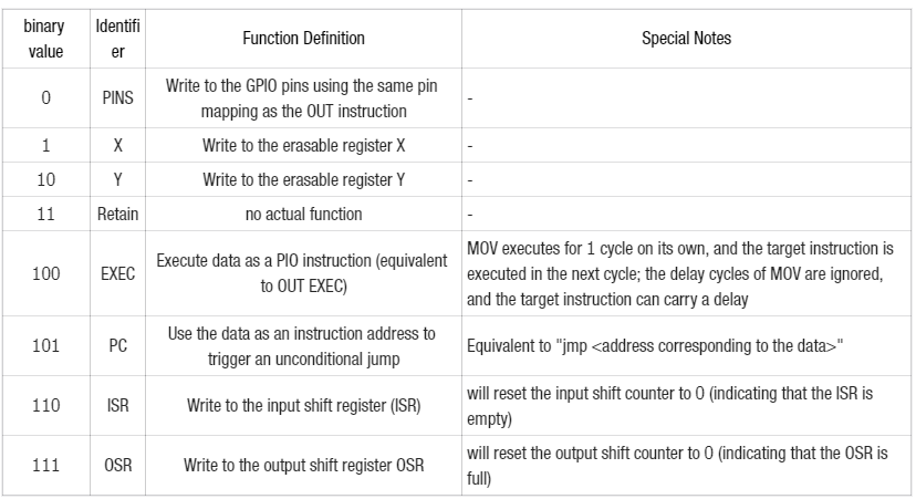
Destination is defined as follows, along with its parameters:
binary value
Identifier
Function Definition
Special Notes
0
PINS
Write to the GPIO pins using the same pin mapping as the OUT instruction
-
1
X
Write to the erasable register X
-
10
Y
Write to the erasable register Y
-
11
Retain
no actual function
-
100
EXEC
Execute data as a PIO instruction (equivalent to OUT EXEC)
MOV executes for 1 cycle on its own, and the target instruction is executed in the next cycle; the delay cycles of MOV are ignored, and the target instruction can carry a delay
101
PC
Use the data as an instruction address to trigger an unconditional jump
Equivalent to "jmp <address corresponding to the data>"
110
ISR
Write to the input shift register (ISR)
will reset the input shift counter to 0 (indicating that the ISR is empty)
111
OSR
Write to the output shift register OSR
will reset the output shift counter to 0 (indicating that the OSR is full)
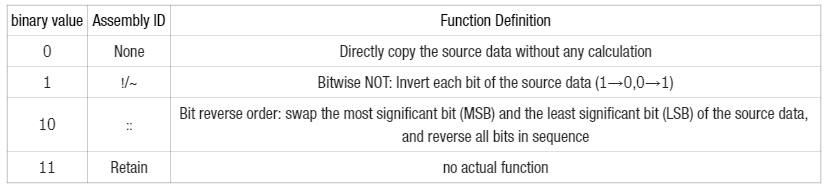
Operation has the following meaning and parameters:
binary value
Assembly ID
Function Definition
0
None
Directly copy the source data without any calculation
1
!/~
Bitwise NOT: Invert each bit of the source data (1→0,0→1)
10
::
Bit reverse order: swap the most significant bit (MSB) and the least significant bit (LSB) of the source data, and reverse all bits in sequence
11
Retain
no actual function
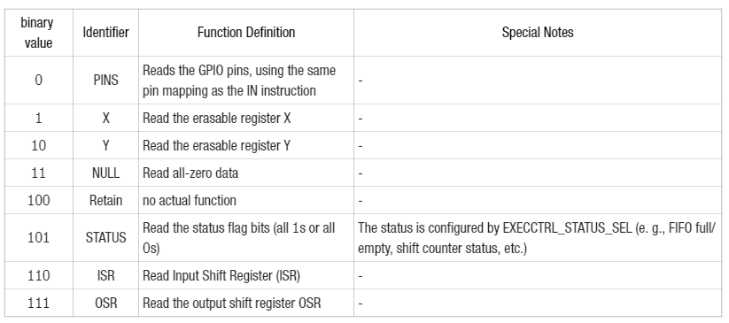
Source has the following meaning and parameters:
binary value
Identifier
Function Definition
Special Notes
0
PINS
Reads the GPIO pins, using the same pin mapping as the IN instruction
-
1
X
Read the erasable register X
-
10
Y
Read the erasable register Y
-
11
NULL
Read all-zero data
-
100
Retain
no actual function
-
101
STATUS
Read the status flag bits (all 1s or all 0s)
The status is configured by EXECCTRL_STATUS_SEL (e. g., FIFO full/empty, shift counter status, etc.)
110
ISR
Read Input Shift Register (ISR)
-
111
OSR
Read the output shift register OSR
-
The assembly syntax is as follows: mov <destination>, (op) <source>
Wherein:
<destination> is one of the aforementioned data migration destinations
<op> If any, it shall be one of the following values:
! or ~ denotes NOT
:: indicates reversing the order of data bits
<source> is one of the aforementioned sources
8. IRQ Interrupt Write or Clear Instruction
The IRQ interrupt write or clear instruction is used to trigger an interrupt or clear a triggered interrupt.
The parameters are defined as follows:
Clear : Clear is a 1-bit configuration bit that determines whether to perform a "clear" or "set" operation on the IRQ flag bit, and has the highest priority (if Clear= 1, the Wait parameter is ignored);
Wait: Wait is a 1-bit configuration bit that takes effect only when Clear= 0 (IRQ is set), and it determines whether to wait for the flag bit to be cleared;
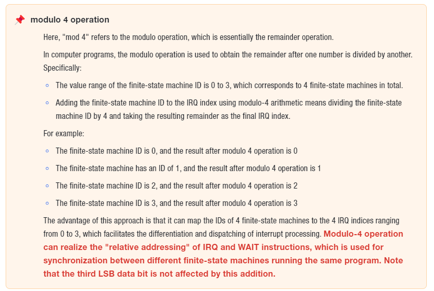
Index : Index is a 5-bit configuration field, where the least significant 3 bits (LSB) specify the IRQ index (0~7), and the most significant bit (MSB) controls whether relative addressing (modulo-4 operation) is enabled:
Base Index: The lowest 3 bits directly correspond to IRQ indices 0 to 7, specifying the IRQ flag bit to be operated on;
Relative addressing (MSB= 1): Add the finite-state machine ID (0~3) to the least significant two bits of the IRQ index, perform modulo 4 on the result, replace the least significant two bits of the original index with the result, and keep the third least significant bit (LSB) unchanged.
Clear The parameters are defined as follows:
Clear value
Operation Type
Function Definition
0 (default)
Set (set to 1)
Set the specified IRQ flag to 1 to trigger an interrupt/synchronization signal
1
Clear (set to 0)
Clear the specified IRQ flag bits to 0 to terminate the interrupt/synchronization signal
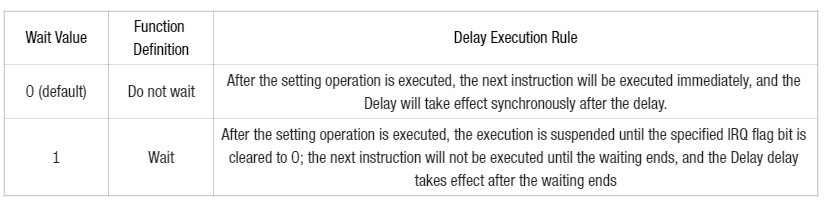
Wait The parameters are defined as follows:
Wait Value
Function Definition
Delay Execution Rule
0 (default)
Do not wait
After the setting operation is executed, the next instruction will be executed immediately, and the Delay will take effect synchronously after the delay.
1
Wait
After the setting operation is executed, the execution is suspended until the specified IRQ flag bit is cleared to 0; the next instruction will not be executed until the waiting ends, and the Delay delay takes effect after the waiting ends
The assembly syntax is as follows:
irq <op> <irq_num> (_rel)
Wherein:
<op>: Optional operation identifier that determines the instruction behavior (set / clear / wait);
<irq_num>: IRQ number (0~7), corresponding to the lowest 3 bits of Index;
_rel: Optional, enables relative addressing (corresponding to MSB of Index = 1), the actual IRQ number is calculated as "(the least significant two bits of irq_num + finite-state machine ID) % 4"(the third LSB bit remains unchanged).
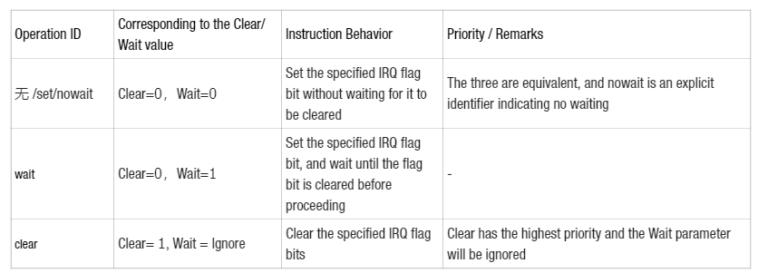
Operation ID
Corresponding to the Clear/Wait value
Instruction Behavior
Priority / Remarks
无 /set/nowait
Clear=0,Wait=0
Set the specified IRQ flag bit without waiting for it to be cleared
The three are equivalent, and nowait is an explicit identifier indicating no waiting
wait
Clear=0,Wait=1
Set the specified IRQ flag bit, and wait until the flag bit is cleared before proceeding
-
clear
Clear= 1, Wait = Ignore
Clear the specified IRQ flag bits
Clear has the highest priority and the Wait parameter will be ignored
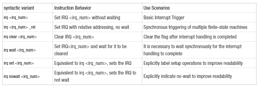
The common usages are as follows:
syntactic variant
Instruction Behavior
Use Scenarios
irq <irq_num>
Set IRQ <irq_num> without waiting
Basic Interrupt Trigger
irq <irq_num> _rel
Set IRQ with relative addressing, no wait
Synchronous triggering of multiple finite-state machines
irq clear <irq_num>
Clear IRQ <irq_num>
Clear the flag after interrupt handling is completed
irq wait <irq_num>
Set IRQ<irq_num> and wait for it to be cleared
It is necessary to wait synchronously for the interrupt handling to complete
irq set <irq_num>
Equivalent to irq <irq_num>, sets the IRQ
Explicitly label setup operations to improve readability
irq nowait <irq_num>
Equivalent to irq <irq_num>, sets the IRQ to not wait
Explicitly indicate no-wait to improve readability
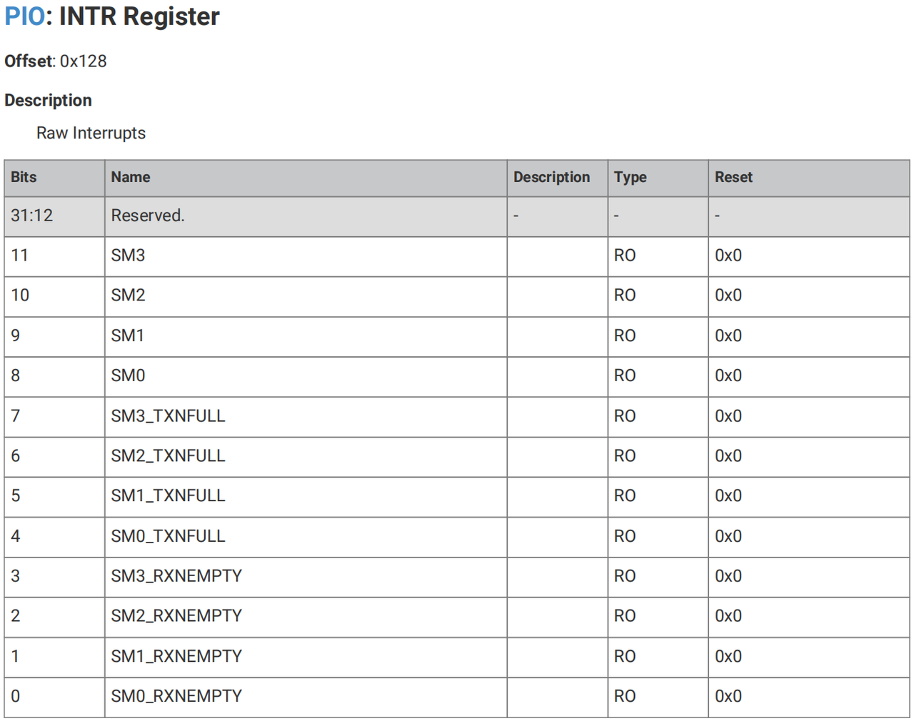
You can check the original interrupt output status in the INTR register:
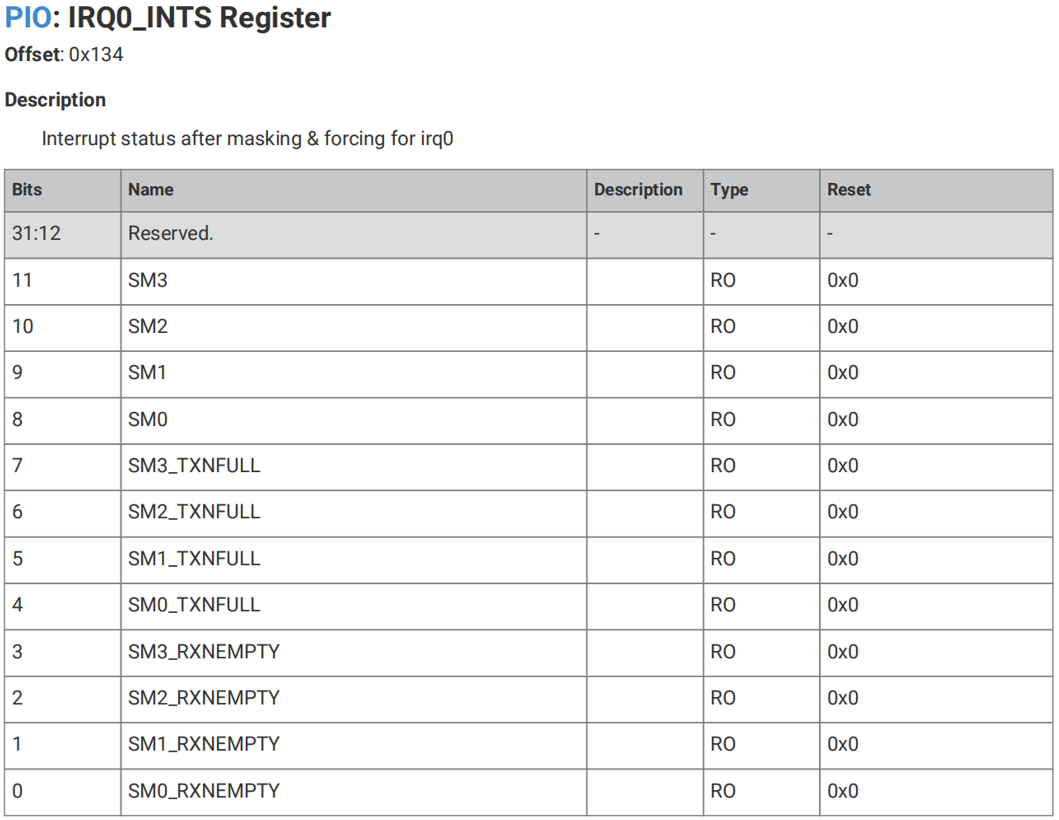
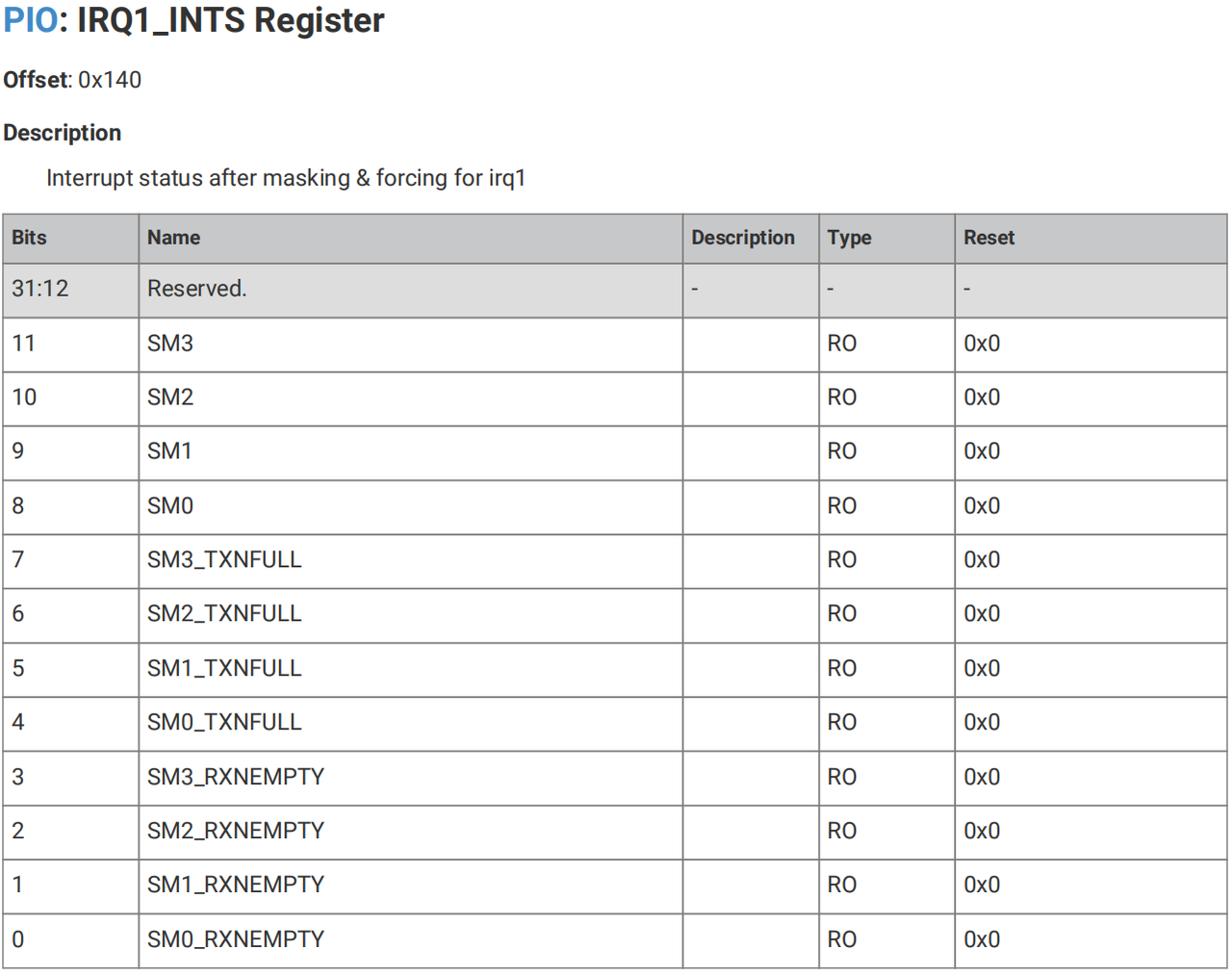
You can check the masked interrupt output status via the INTS register:
9. SET Instruction for GPIO Mapping Configuration
The SET instruction for setting GPIO mapping is used to write data to GPIO pins (i. e., control high and low levels), and can also write data to X\Y registers.
Write the immediate value Data to Destination.
The parameters are defined as follows:
Destination: Destination is a 3-bit configuration bit that specifies the write target of the 5-bit immediate value;
Data: Data is a 5-bit configuration bit, which is a fixed value written directly to the target, with a value range of 0 to 31 (the maximum value of 5-bit binary):
If the target is PINS / PINDIRS: each bit of Data corresponds to one GPIO in the SET pin mapping, and a bit value of 1/0 corresponds to the high/low level (for PINS) or output/input direction (for PINDIRS) of the GPIO;
If the target is X / Y: Data is directly used as the lower 5 bits of the register, and the upper 27 bits are cleared to 0. Therefore, the maximum value that can be initialized for X/Y via SET is 31 (suitable for short-period loop counting).
This instruction is used to set control signals, such as clock or chip select, or to initialize a loop counter. Since Data has only 5 data bits, the value that the erasable register can SET ranges from 0 to 31, allowing a maximum of 32 loops.
SET and OUT have independently configurable pin mappings. They can be mapped to different pins, for example, one pin for the clock signal and the other for data. Their pin ranges can also overlap: a UART transmission routine can use SET to set the start and stop bits, and use the OUT instruction to shift out FIFO data on the same pin.
The assembly syntax is as follows: set <destination>, <value>
Wherein:
<destination> is the destination for the aforementioned data operations;
<value> is the value to be set, and its valid range is 0 to 31.