RP2040 PIO: Hardware Architecture & Working Principles Quick Overview
RP2040 PIO is a programmable‑IO peripheral with two blocks and eight state‑machines, implementing diverse serial/parallel protocols with minimal CPU overhead.
COMPONENTS
PROJECT DESCRIPTION
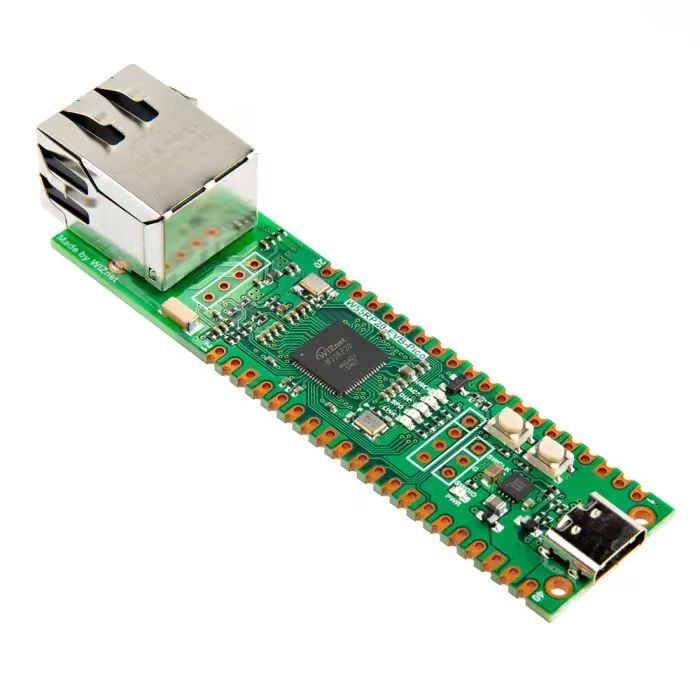
【Preliminary Note】The original hardware example in this article was written based on the RP2040. The actual hardware used in this hands-on demonstration features the W55RP20 as the main controller chip. The circuit logic and UF2 flashing operation principles are universally applicable, with only the main controller model differing. The original chip model mentioned in the circuit descriptions below is provided for reference purposes only.
Tweet
1. Hardware Explanation
It is not difficult to see that for the RP2040 onboard the Raspberry Pi Pico board, its communication peripheral resources are very limited. When the number of communication peripherals we need to use exceeds the number of communication peripherals available on the Raspberry Pi Pico (for example, four UARTs are required), or when the Communication Protocol we need is not supported by the hardware on the Raspberry Pi Pico (for example, VGA video output), in addition to using GPIO software to simulate and implement the communication interface, we can also select the PIO programmable input/output interface.
PIO (Programmable Input/Output) is a special peripheral of the RP2040 microcontroller. The term "programmable input/output" means that it can process data input to or output from specific GPIO pins using preconfigured operations without requiring intervention from the RP2040's CPU.It can implement a variety of different communication interfaces/peripherals. In fact, we can regard PIO as another simple and independent microcontroller inside the RP2040 chip. By writing simple assembly programs into the PIO block, multiple communication interfaces can be implemented. Meanwhile, compared with the GPIO software-emulated Communication Protocol, it hardly occupies CPU resources and features a high operating speed.
Currently, the PIO peripheral supports the following Communication Protocols: 8080 and 6800 parallel buses, I2C, 3-pin I2S, SDIO, SPI, DSPI, QSPI, UART, DPI or VGA (via a resistive DAC).
1.1 Basic Structure of PIO Peripherals
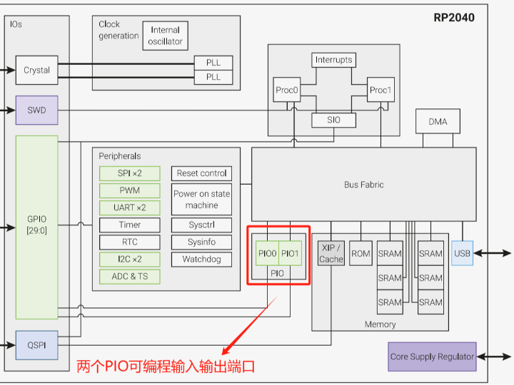
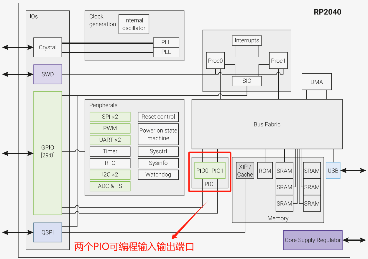
The RP2040 features two identical PIO peripherals, each of which is independently connected to the AHB-Lite bus, GPIO pins, and interrupt controller:
AHB Lite bus: enables high-speed data interaction between PIO and the main CPU of RP2040 as well as on-chip memory;
GPIO pins: the physical interfaces through which the PIO performs input/output operations with external devices;
Interrupt Controller: Implements the function of the PIO sending interrupt requests to the main CPU to complete event synchronization.
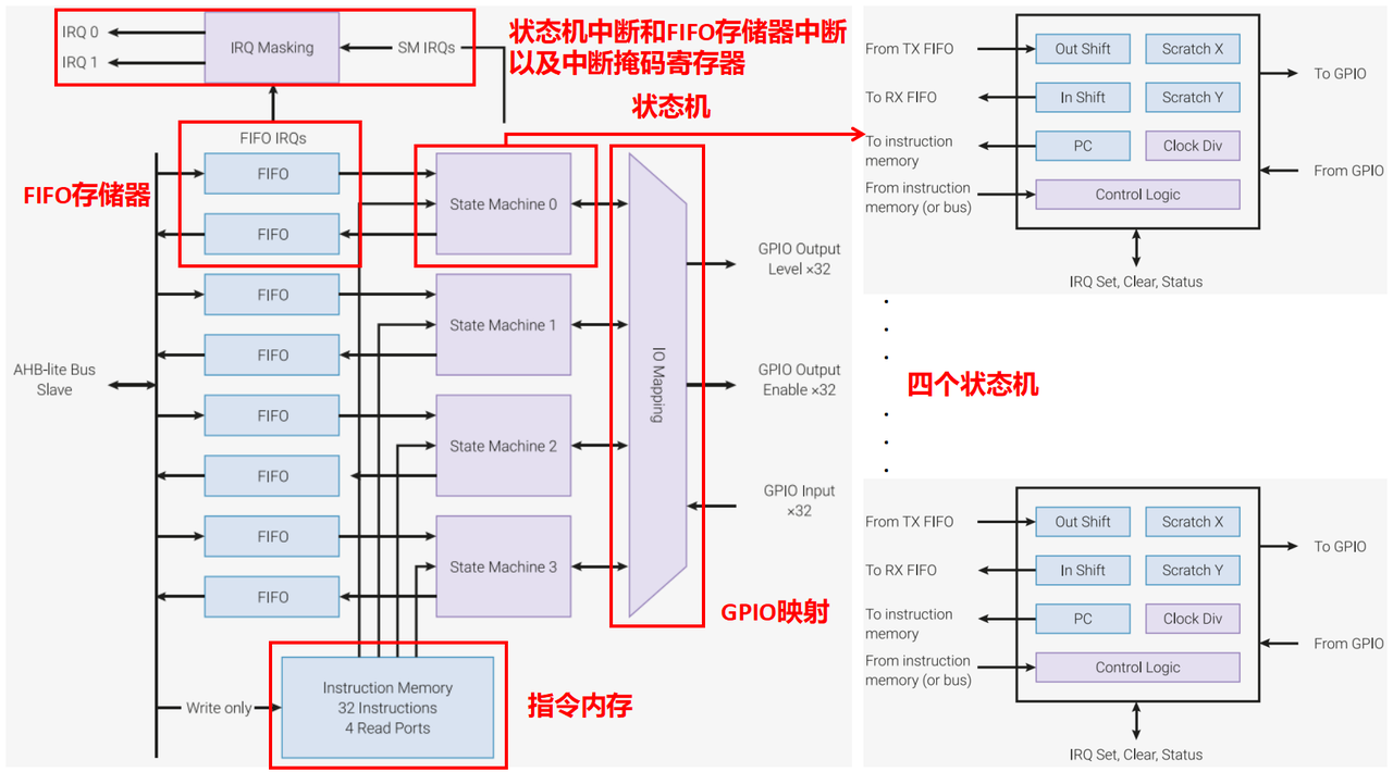
The structural diagram of a single PIO peripheral is shown below:
Simply put, the PIO peripheral consists of the following components:
finite-state machine (State Machine): Each PIO contains 4 independent finite-state machines, which are the core execution hardware of the PIO and can be regarded as a lightweight dedicated processor, with the following internal components:
PC (Program Counter): Records the address of the instruction to be executed currently in the instruction memory, and controls the sequential execution of instructions;
Clock Div (Clock Divider): Independently adjusts the operating clock frequency of the finite-state machine to adapt to external I/O protocols of different rates;
X/Y Erasable Data Register: Temporarily stores operation data and intermediate results;
Out Shift (Output Shift Register): Shifts data according to the specified bit width and sequence, then outputs it to GPIO;
In Shift (Input Shift Register): Reads data from GPIO and performs shift buffering according to specified rules;
The finite-state machine reads assembly instructions in the instruction memory via internal registers, and autonomously completes operations such as data read/write and GPIO control; meanwhile, it can access modules including FIFO, DMA and GPIO, and generate interrupt signals for synchronization between finite-state machines as well as between PIO and the main CPU.
Instruction Memory: it is a read-only memory unit with a capacity of 32 instructions, shared by 4 finite-state machines within the same PIO. The PIO-specific assembly instructions written by users will be loaded into this memory for each finite-state machine to read and execute independently.
GPIO Mapping:
The input/output signals of the finite-state machine can be mapped to the GPIO pins of the RP2040 (the hardware supports up to 32 GPIOs, while the RP2040 actually leads out 30 available GPIOs);
All finite-state machines within the same PIO can independently and simultaneously access any GPIO pin, featuring flexible pin allocation capabilities.
FIFO Memory: The Out Shift and In Shift shift registers of each finite-state machine are respectively connected to a set of "Transmit FIFO (Tx FIFO)" and "Receive FIFO (Rx FIFO)", whose core function is to realize the asynchronous decoupling between "data transmission and reception requests" and "actual execution operations":
Transmission Scenario: The main CPU first writes the data to be output to the Tx FIFO; when the finite-state machine is ready, it fetches data from the Tx FIFO and outputs it to the GPIO via the Out Shift register.
Reception Scenario: The finite-state machine temporarily stores the data read from the GPIO into the In Shift register, then writes it to the Rx FIFO; the main CPU can fetch the data from the Rx FIFO at an appropriate time.
Interrupt and Interrupt Mask Registers: Used to manage the interrupt signals of PIO:
Interrupt sources: including raw interrupt signals from FIFOs (e. g., FIFO full/empty) and finite-state machines (e. g., instruction execution completion, specific operation trigger);
Interrupt Mask Register: It configures the original interrupt signals to be either "enabled or masked", and only unmasked interrupts are sent to the RP2040 interrupt controller to trigger the response of the main CPU.