Raspberry Pi Pico UART Deep Dive: Hardware Architecture & Register Operations
This article details Raspberry Pi Pico UART hardware architecture, covering FIFO buffer, DMA, interrupts, baud rate calculation and hardware flow control.
COMPONENTS
PROJECT DESCRIPTION
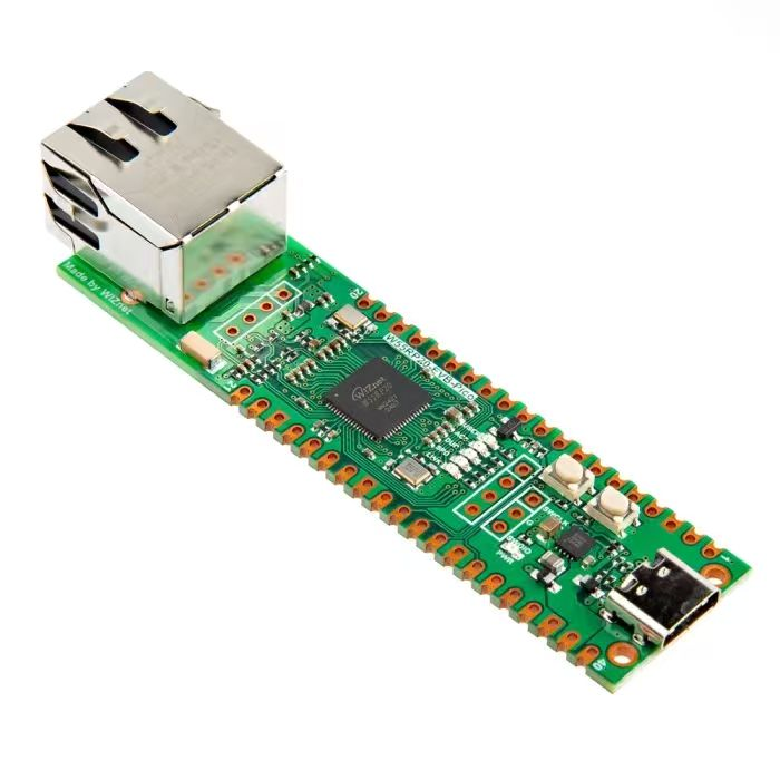
【Preliminary Note】The original hardware example in this article was written based on the RP2040. The actual hardware used in this hands-on demonstration features the W55RP20 as the main controller chip. The circuit logic and UF2 flashing operation principles are universally applicable, with only the main controller model differing. The original chip model mentioned in the circuit descriptions below is provided for reference purposes only.
The UART serial port peripheral on the Raspberry Pi Pico is the "serial communication unit" on the Raspberry Pi Pico, which is specifically responsible for the communication between the Pico and other devices (such as computers, sensors, and displays) via the serial port protocol:
Data transmission: The parallel data inside Pico is converted into serial data via UART and then transmitted to external devices;
Data reception: The serial data from external devices is converted into parallel data via UART and transmitted to the interior of Pico.
The serial port peripheral is not an independently operating unit, but a working module that needs to cooperate with other internal components of the Pico:
CPU: Responsible for issuing instructions and processing final data;
UART peripheral: responsible for serial-parallel conversion of data and serial codec of different devices;
AMBA APB bus: The CPU controls the UART peripheral and transmits data via the AMBA APB bus;
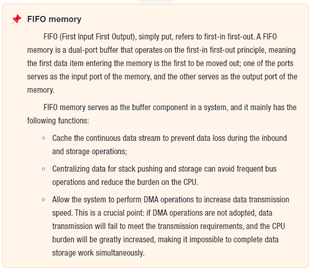
FIFO Memory: The data received and transmitted by the UART can be buffered by the FIFO memory, and the FIFO buffer supports independent storage of up to 32 bytes of data in both transmission and reception modes.
The serial peripheral supports the following functions:
Programmable baud rate generator: It generates a clock signal matching the target communication rate to realize "baud rate synchronization" between the UART and external devices (e. g., 9600,115200, etc.), which serves as the foundation of asynchronous communication;
It provides functions similar to the industry-standard 16C650 UART device: It complies with the universal UART hardware protocol, ensuring that the UART of Pico can directly communicate with mainstream UART devices such as computers and sensors, and boasts excellent interoperability;
When the system clock is 125MHz, the maximum supported rate is 7.8Mbps: This refers to the theoretical upper bandwidth limit of UART; the commonly used low-speed communication (e. g., 9600bps) in daily scenarios is far lower than this value, which can meet the transmission requirements of most scenarios.
Independent maskable interrupts derived from reception, transmission, modem mode and error conditioning: The UART provides independent interrupt sources for events such as "reception complete, transmission complete, modem status change, and communication errors"; the CPU can mask specific interrupts via registers to only respond to required events, thus reducing unnecessary CPU resource consumption;
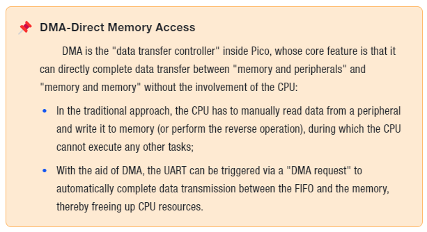
Sending DMA Requests to the DMA Controller: The UART can initiate a "data transfer request" to the DMA controller to trigger the DMA to complete "data transfer between the FIFO and the memory"(without CPU intervention), thus reducing the load on the CPU;
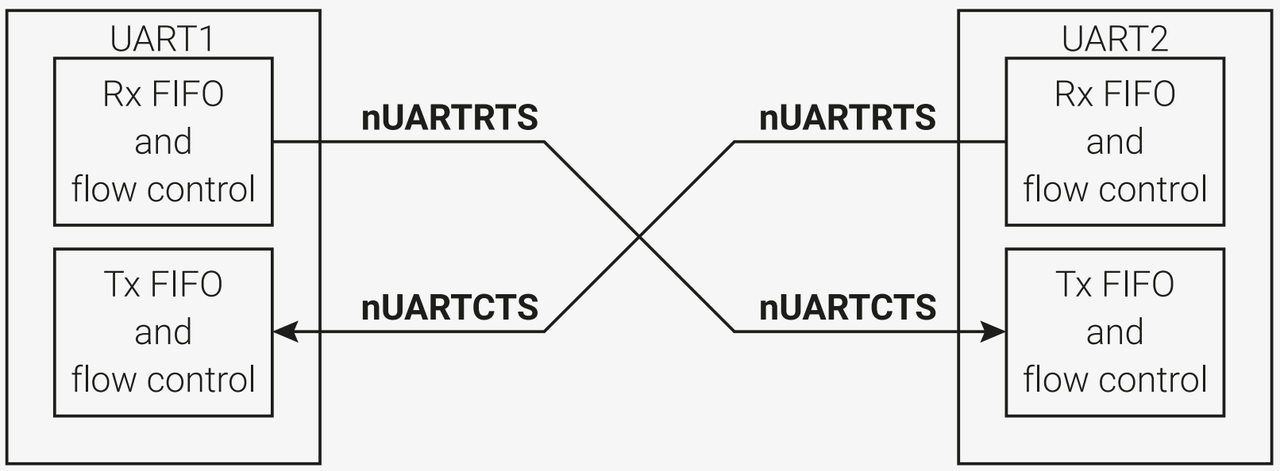
It features a programmable hardware flow control: Byte Flow Control between the transmitter and receiver is implemented via the nUARTCTS (Clear To Send) and nUARTRTS (Request To Send) pins: when the receiver buffer is full, it notifies the transmitter to suspend transmission through the CTS pin; once the receiver is ready, it re-enables transmission via the CTS pin to prevent data overflow.
When the UART receives data, if an abnormality occurs, it will mark and protect the data via registers:
If a frame error, parity error, or break error occurs: the UART will set the corresponding "error flag bit" in the register, and meanwhile store the error data into the receive FIFO for subsequent processing by the CPU;
If a FIFO overflow occurs (the amount of received data exceeds the FIFO capacity): the UART will immediately set the "overflow flag bit" and stop receiving new data to prevent the valid data already stored in the FIFO from being overwritten.
1. UART Peripheral Architecture
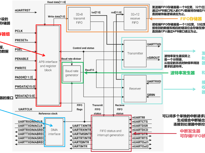
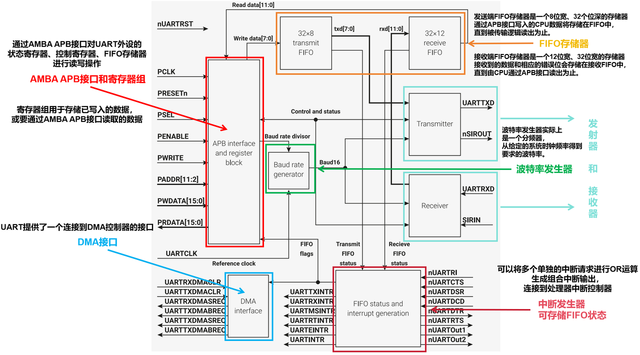
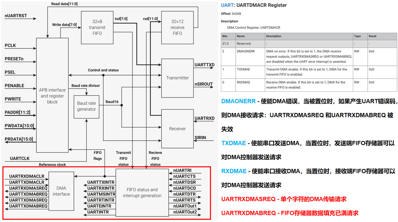
The basic structural block diagram of the serial port peripheral of Raspberry Pi Pico is as follows:
The block diagram above illustrates the "internal working pipeline" of the UART serial peripheral on the Raspberry Pi Pico, where each module has a clear division of labor to collectively implement serial communication:
Core control entry: AMBA APB interface and register file, which serves as the only window for CPU to communicate with UART:
AMBA APB Interface: CPU sends "control commands"(e. g., setting baud rate), writes "data to be transmitted", or reads "received data" and "UART operating status" to the UART through this interface;
Register File: It stores the control parameters (e. g., baud rate configuration) and status information (e. g., whether the FIFO is full) of the UART, as well as temporary data — it serves as the "control panel + temporary notepad" for the UART.
Clock Synchronization Core: Baud Rate Generator
It serves as the UART "metronome", responsible for generating clock signals that match the target baud rate;
Operating logic: Starting from the system clock (UARTCLK), the Baud16 clock (used in normal mode) is generated through frequency division — Baud16 is a clock that runs at 16 times the target baud rate (for example, if the target baud rate is 9600, then Baud16 is 153600);
Function: The transmitter/receiver will divide Baud16 by 16 to obtain a "1x baud rate" clock, which is used for synchronous data transmission/reception (during reception, sampling can be performed in the middle of each data bit to reduce level judgment errors).
Data Buffer: FIFO Memory:
It is divided into transmit FIFO and receive FIFO, which is the key to alleviating the " CPU and UART rate mismatch".
Transmit FIFO (32×8 bits): The CPU first writes the 8-bit data to be transmitted here, and the transmitter will take the data byte by byte from the FIFO and convert it into serial data for transmission; even if the CPU has a slow processing speed, the data can be temporarily stored without being lost;
Receive FIFO (32×12 bits): After the receiver converts the received serial data into parallel data, it stores the data together with the "error flag bits"(such as frame error) here (the 12 bits consist of 8 bits of data + 4 bits of error information), waiting for the CPU to read, so as to prevent data loss caused by the CPU being busy when the receiver receives data.
Data Transceiving Execution: Transmitter & Receiver
This is the "execution unit" of the UART, which is responsible for serial-to-parallel conversion;
Transmitter: Reads parallel data from the transmit FIFO, and under the synchronization of the Baud16 clock, converts the data bit by bit into a serial signal, and sends it out from the UARTTXD pin;
Receiver: Receives serial signals from the UART RXD pin, and under the synchronization of the Baud16 clock, converts the signals bit by bit into parallel data and stores them in the receive FIFO (while marking the error status).
Status Notification: Interrupt Generator
It acts as the "status announcer" of the UART;
Collect signals such as the status of FIFO (e. g., transmit FIFO empty, receive FIFO full), transmit/receive events (e. g., transmission complete, reception complete), and communication errors (e. g., frame error);
These signals are subjected to an "OR operation"(i. e., triggered if any one of the events occurs) to generate an interrupt signal that is sent to the CPU for timely processing, such as reading received data and handling errors.
Efficient Data Transfer: DMA Interface
This serves as the "connection interface" between the UART and the DMA controller;
When the data volume in the FIFO reaches a certain threshold, the UART will initiate a "transfer request" to the DMA through this interface;
Upon receiving a request, DMA will automatically transfer data between the transmit FIFO and the memory as well as between the receive FIFO and the memory, eliminating the need for CPU participation throughout the process and thus reducing CPU load.
The overall workflow is as follows:
Transmission Flow: CPU writes data to the transmit FIFO via the APB interface → the baud rate generator generates the Baud16 clock → the transmitter fetches data from the FIFO → converts the data into serial signals and outputs them through UARTTXD;
Reception Process: UARTRXD receives serial data → the receiver (using Baud16 clock) converts it to parallel data and adds error flags → the data is stored in the receive FIFO → the interrupt generator notifies the CPU → the CPU (via APB interface) reads the data from the receive FIFO.
Here, the baud rate generator provides two clock signals, IrLPBaud16 and Baud16:
IrLPBaud16: This is the clock signal provided to the serial port transmitter and receiver, which is used in the IrDA infrared mode and will not be elaborated here.
Baud16: A clock signal provided to the UART transmitter and receiver, which generates an integer baud rate reference clock at 16× the baud rate with a pulse width of one UARTCLK clock cycle. Used in normal mode, this clock signal is divided by 16 to generate the clock for the UART transmitter.
2. Clock Configuration of UARTCLK
The frequency of UARTCLK needs to adapt to the range of the baud rate:
16 × maximum baud rate ≤ UARTCLK frequency ≤ 6×65535× minimum baud rate
For example, when the baud rate ranges from 110 to 460800, the UARTCLK frequency must be between 7.3728 MHz and 115.34 MHz.
Meanwhile, the ratio of the frequency of UARTCLK to the frequency of PCLK must be less than or equal to 5/3, that is:
The frequency of UARTCLK ≤ 5/3 × the frequency of PCLK
For example, in UART mode, when UARTCLK is 14.7456MHz and a baud rate of 921600 is to be generated, PCLK must be greater than or equal to 8.85276MHz. This ensures that the UART has sufficient time to write the received data into the receive FIFO.
3. UART Peripheral Operation
The base addresses of the UART0 and UART1 registers are 0x40034000 and 0x40038000 respectively.
The UART peripheral can be controlled by writing to the UARTLCR register, which contains 30 bits internally. It should be noted that we need to access the UARTLCR_H, UARTIBRD and UARTFBRD registers externally through the APB bus interface to write to the UARTLCR register, in which:
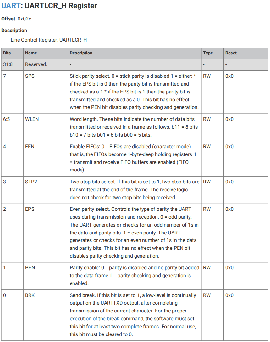
UARTLCR_H Register:
It is mainly used to define valid data for transmission, data bits, stop bits, parity bits, transmission stream mode and disconnection.
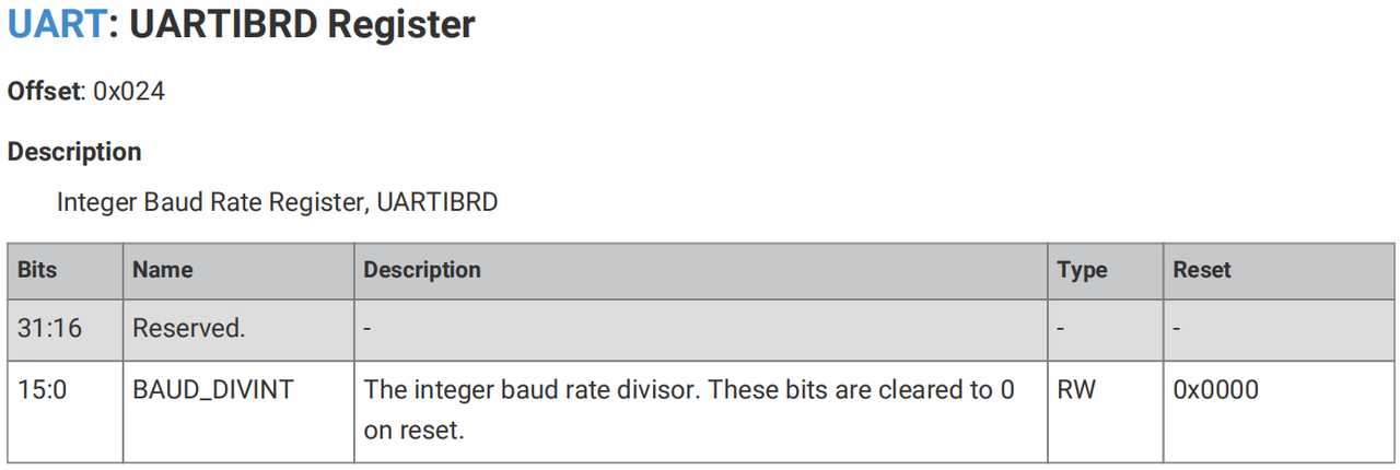
UARTIBRD Register: defines the integer part of the baud rate divisor.
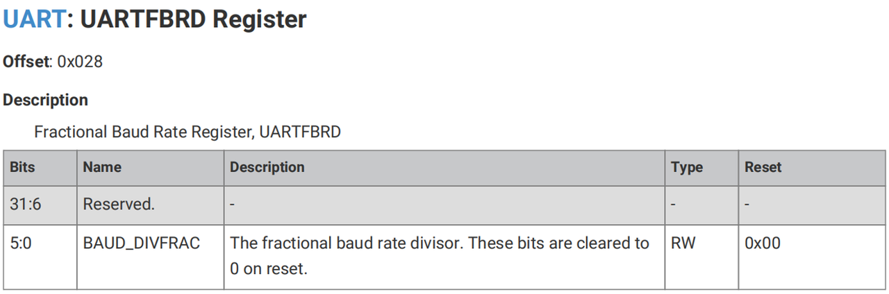
UARTFBRD Register: defines the fractional part of the baud rate divisor
3.1 Set the Baud Rate
Setting the baud rate mainly involves configuring the baud rate divisor factor (hereinafter referred to as the baud rate factor), which is a 22-bit number consisting of a 16-bit integer part and a 6-bit fractional part. The fractional baud rate factor allows any clock with a frequency higher than 3.6864 MHz to be used as UARTCLK while still being able to generate all standard baud rates.
The 16-bit integer baud rate factor is loaded via the UARTIBRD register, while the 6-bit fractional baud rate factor is loaded via the UARTFBRD register.
The relationship between the baud rate factor and the UARTCLK clock is as follows:
BRD = BRDI + BRDF = UARTCLK/(16×Baud Rate), where BRDI is the integer part of BRD, BRDF is the fractional part separated by a decimal point, and UARTCLK is the system clock connected to the UART.
3.2 Error Bit
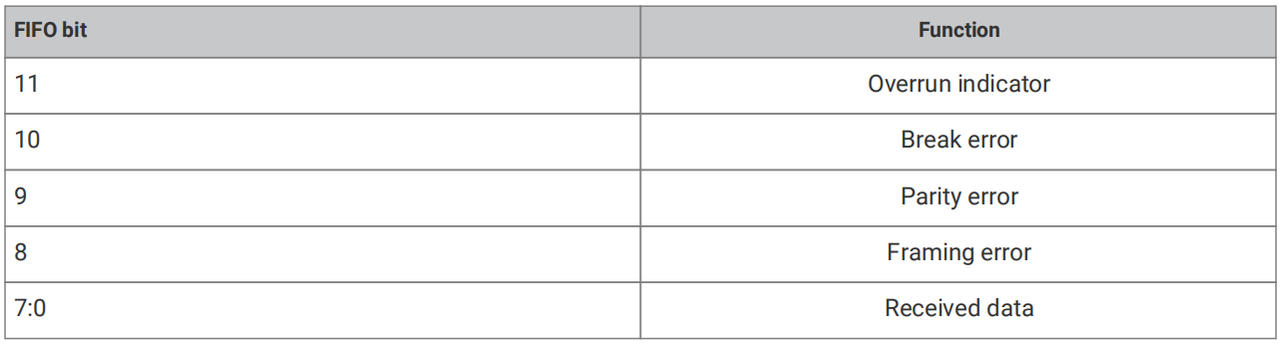
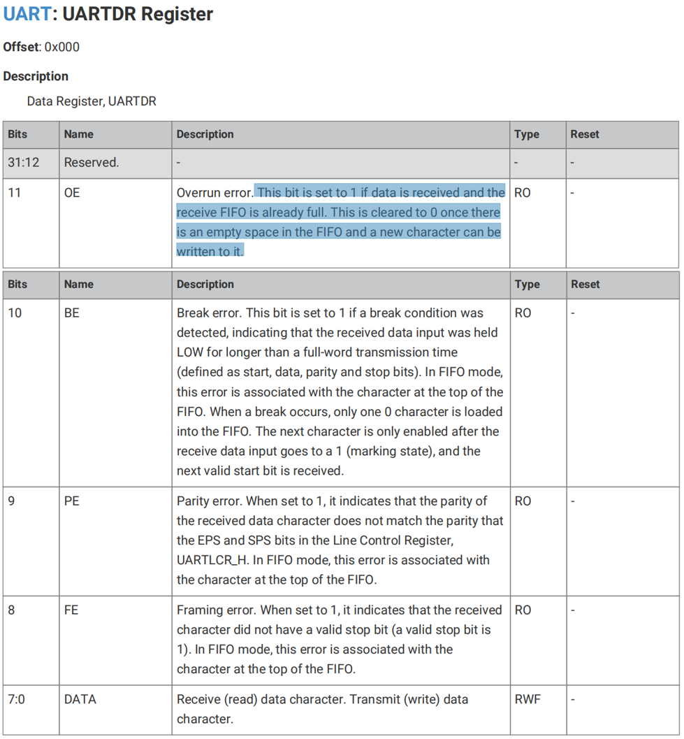
Three error bits are stored in bits [10:8] of the receive FIFO memory and are associated with a specific character. There is also an additional error indicator for the overrun error, which is stored in bit 11 of the receive FIFO.
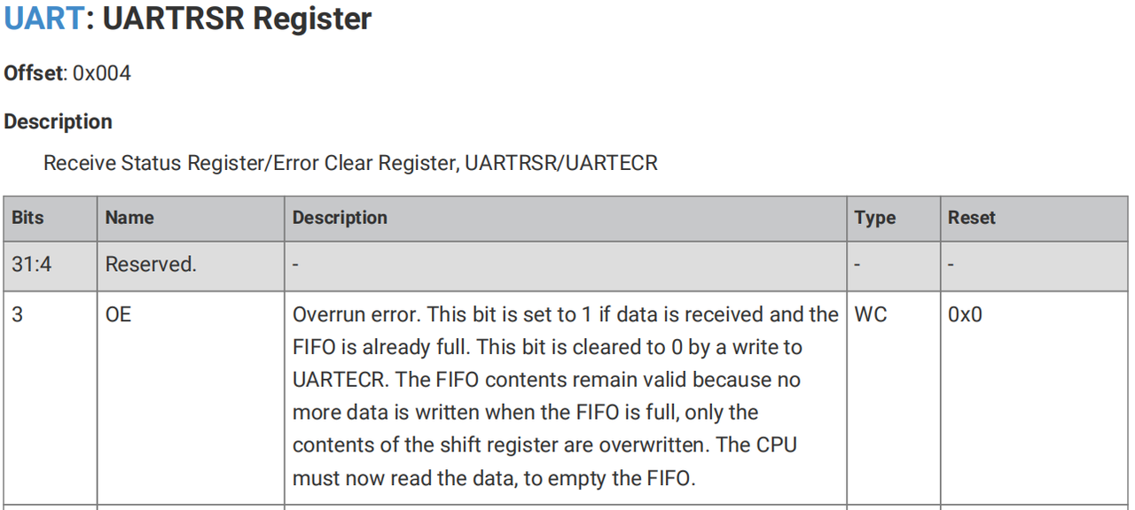
When the FIFO memory is full, the overrun error flag will be set, and the next data will be directly written into the shift register of the UART (the shift register is mainly used for serial-parallel conversion of serial data), overwriting the data currently stored in the UART shift register. When an empty slot in the receive FIFO becomes available and another character is received, the state of the overrun bit, together with the received character, is copied into the receive FIFO, after which the overrun state will be cleared.
Regarding the reading of error bits, it is mainly accomplished by accessing the UARTDR register:
3.3 System Diagnosis and Loopback Test
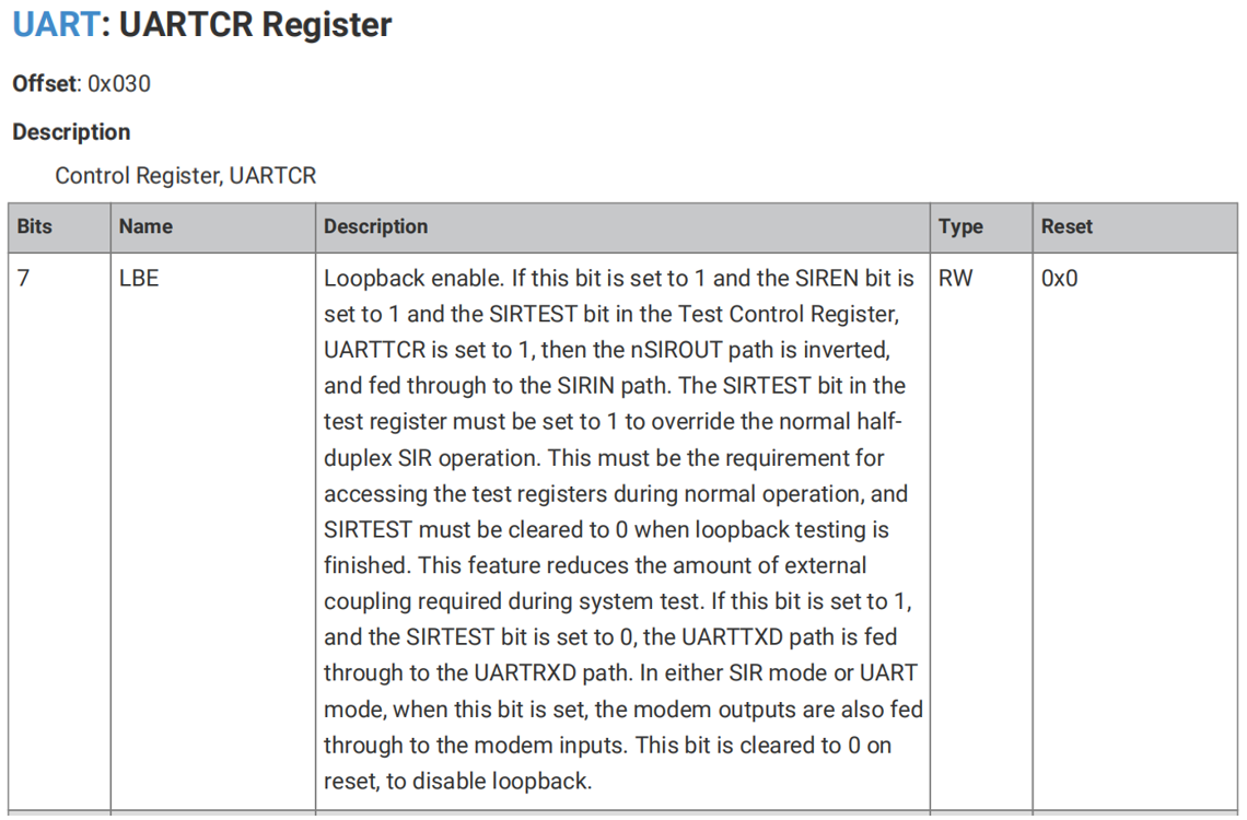
By setting the LBE bit of the UARTCTL register, the UART can be configured in internal loopback mode for diagnostic or debugging purposes. In loopback mode, the transmit data output from UARTxTXD will be received by the UARTxRXD input. Note that the LBE bit shall be set before the UART is enabled.
3.4 FIFO Operations
The UART features two independent FIFO memories: a separate 32×8 Tx transmit FIFO and a 32×12 Rx receive FIFO. Both FIFOs are accessed via the UARTDR register. A read operation to the UARTDR register returns a 12-bit value consisting of 8 data bits and 4 error flag bits, while a write operation loads 8-bit data into the transmit FIFO.
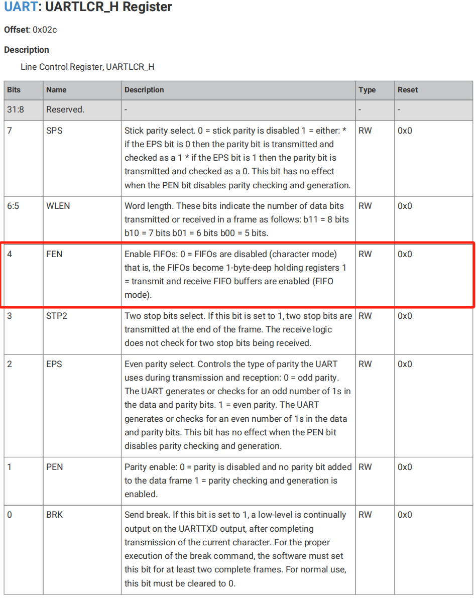
We can control the operating mode of the FIFO by setting the FEN bit in the UARTLCR_H register:
FEN = 0: FIFO is disabled, the device operates in character mode and maintains a 1-byte depth register
FEN = 1: FIFO is enabled, the device operates in FIFO mode, and both the transmit and receive FIFO buffers are activated
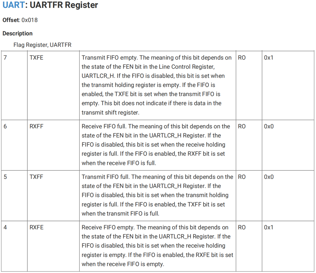
The status of the FIFO can be monitored via the UART Flag (UARTFR) register and the UART Receive Status (UARTRSR) register to check whether it is in an empty, full, or overflow state.
The UARTFR register contains empty and full flag bits (TXFE, TXFF, RXFE, and RXFF bits):
If FIFO is disabled, the empty and full flag bits will be set according to the status of the 1-byte depth register.
The UARTRSR register indicates the overflow status via the OE bit:
4. UART Transmit and Receive Process
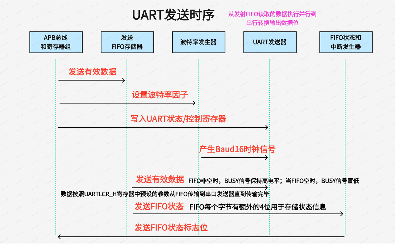
4.1 UART Data Transmission Process
The APB bus can access the status/control registers and store the information to be transmitted into the transmit FIFO memory.
The baud rate generator acquires the baud rate division factor from the APB bus and the register block, and generates the internal clock Baud16, whose frequency is 16 times the baud rate;
The UART transmitter is controlled by the status/control register, and transmits the content in the transmit FIFO memory one by one with Baud16 as the clock source;
The FIFO status and interrupt generator generates corresponding FIFO flag bits and interrupt signals according to the content of the FIFO memory.
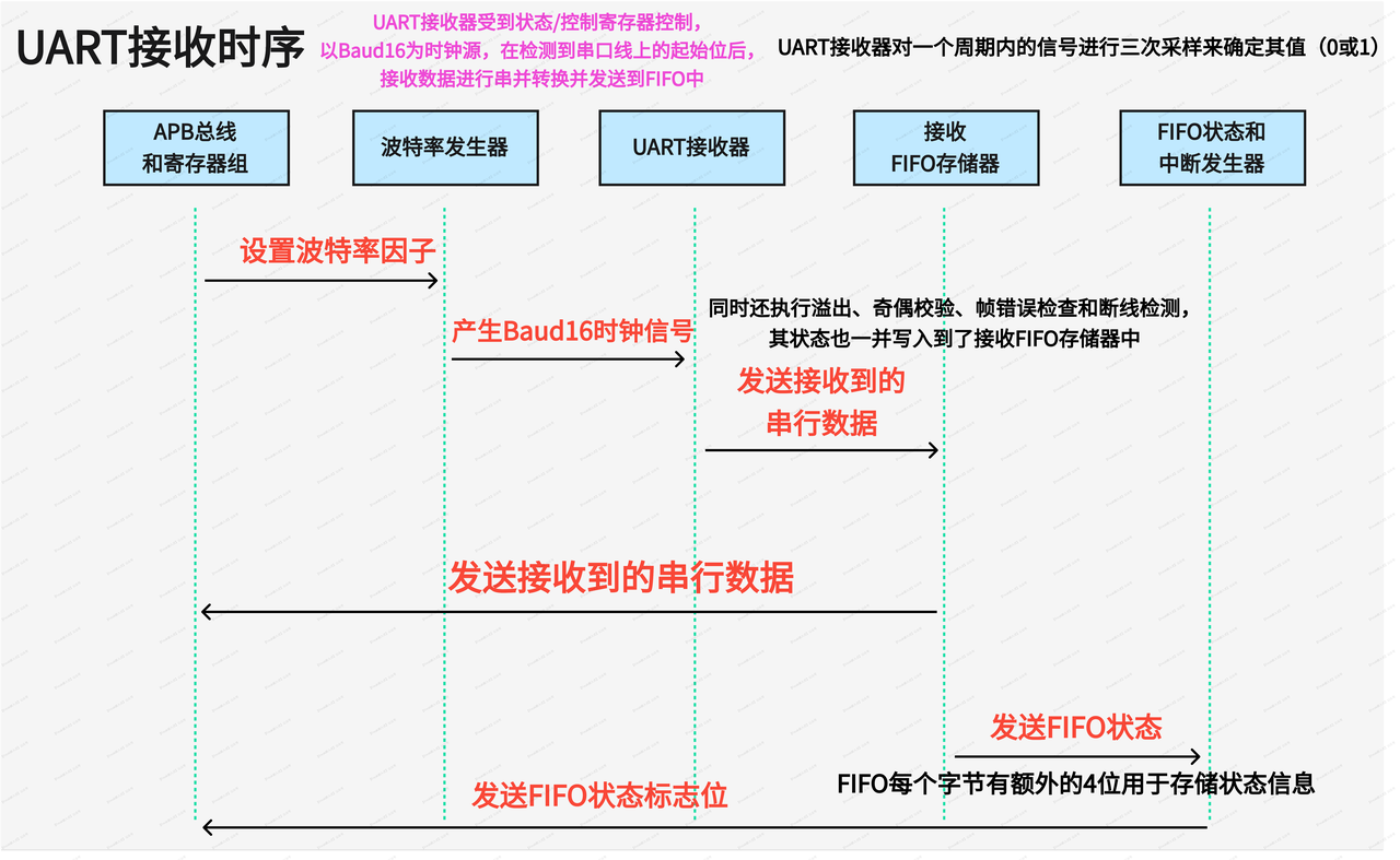
4.2 UART Data Receiving Process
The UART receiver is controlled by the status/control register, uses Baud16 as the clock source, and stores the received data into the receive FIFO memory;
The APB bus can obtain the read value by reading the receive FIFO.
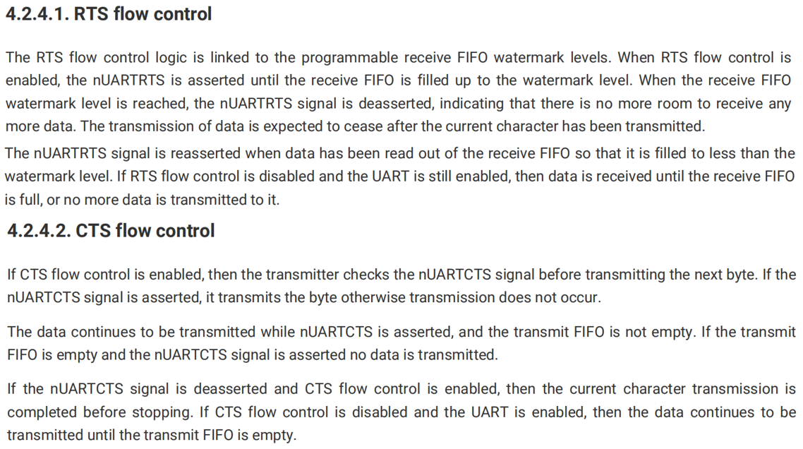
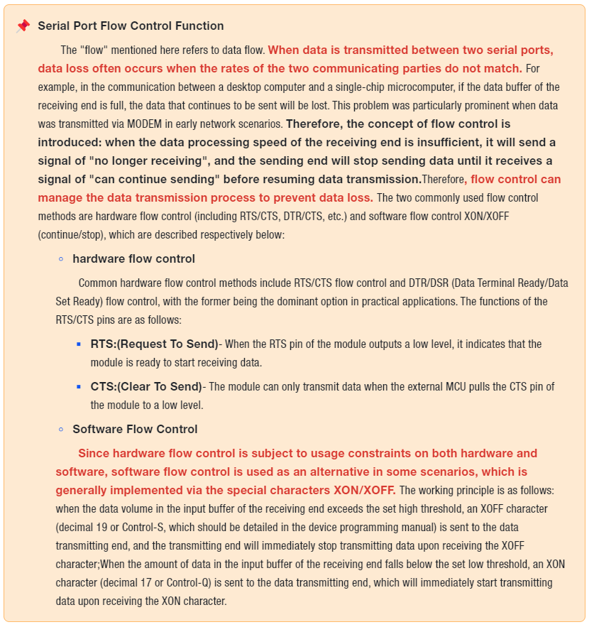
5. UART hardware flow control function
We can control the serial data flow by using the nUARTRTS output and nUARTCTS input signals:
When RTS flow control is enabled, the nUARTRTS output signal will be set to high level (invalid) once the data in the receive FIFO memory is filled to the set buffer depth; before that, the nUARTRTS output signal will always remain at low level (valid) to indicate the FIFO status. When CTS flow control is enabled, the UART transmitter will start transmitting data only after receiving the signal that the external device pulls CTS to low level.
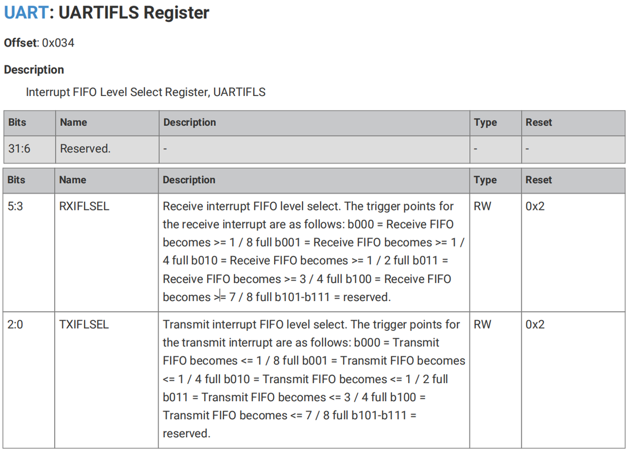
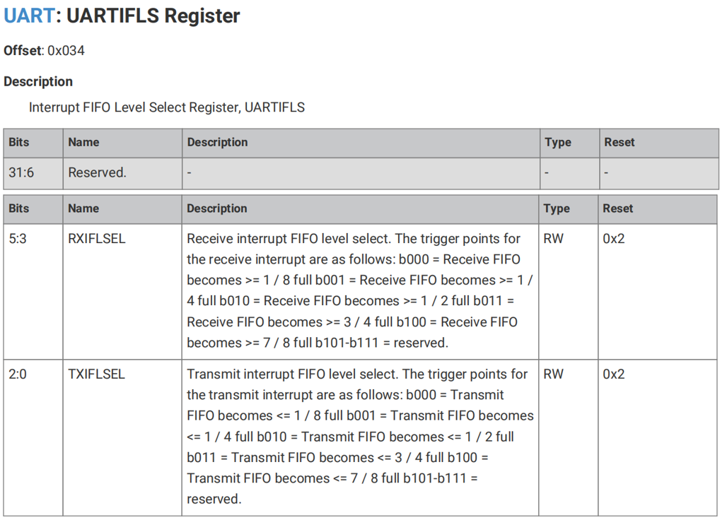
The FIFO memory buffer depth can be configured by setting the UARTIFLS register:
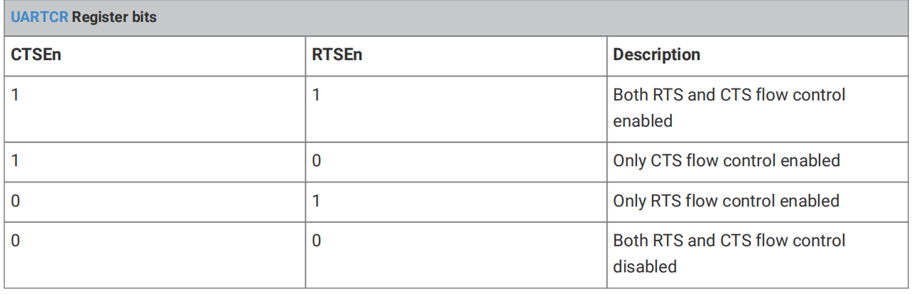
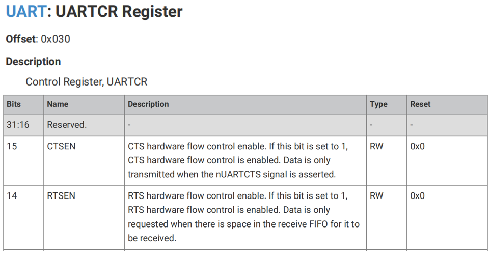
Hardware flow control can be selected by using the RTSEn and CTSEn bits in the UARTCR control register:
It should be noted that once RTS flow control is enabled (i. e., the RTSEN bit is set to 1), the software can no longer use the RTSEn bit in the UART control register (UARTCR) to control the state of nUARTRTS, nor can it change the output value of nUARTRTS.
6. DMA Interface of UART
The UART provides an interface to the DMA controller, with separate transmit and receive channels. DMA operations for the UART are initiated via the UART DMA Control (UARTDMACR) register. DMA performs data transfers in response to DMA request signals, which are issued either after a peripheral completes an event or when the peripheral is ready for operation. These DMA request signals are generated by the data transfer-related registers within the peripheral, which store the peripheral's current operating status and send requests to the DMA when predefined conditions are met.
The DMA requests that can be generated include:
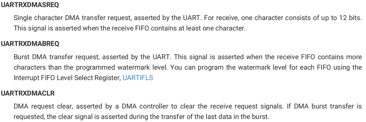
For the receiving end:
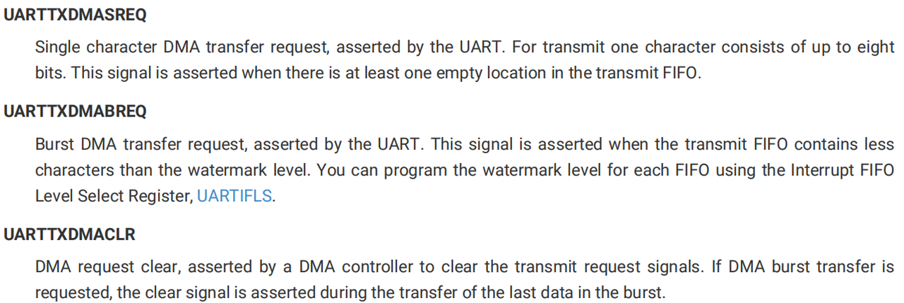
For the sender:
Simply put, for the receiving end, as long as there is data in the receive FIFO, a single transfer request UARTRXDMASREQ will be generated; when the data volume in the receive FIFO is greater than or equal to the UARTIFLS register-configured FIFO buffer depth, a burst transfer request UARTRXDMABREQ will be generated;For the transmitter side, as long as there is at least one empty slot in the transmit FIFO, a single transfer request UARTTXDMASREQ will be generated; and as long as the number of characters contained in the transmit FIFO is less than the FIFO trigger level, a burst request UARTTXDMABREQ will be generated. For both the receiver and transmitter sides, the DMA controller can also generate UARTTXDMACLR and UARTRXDMACLR requests to clear the DMA data transfer request signal after the data transfer is completed.
Meanwhile, various DMA requests can occur simultaneously, and both single and burst transfer requests are automatically processed by the DMA controller; whether data transfer is performed in single mode or burst transfer mode depends on the set FIFO memory buffer depth and the amount of data in the FIFO.
7. Interrupts of UART
7.1 UART Interrupt Types
When any of the following conditions is detected, UART will generate an interrupt:
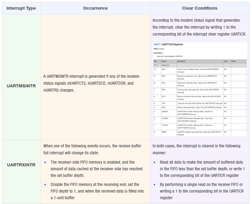
Modem status signal change: generate UARTMSINTR interrupt
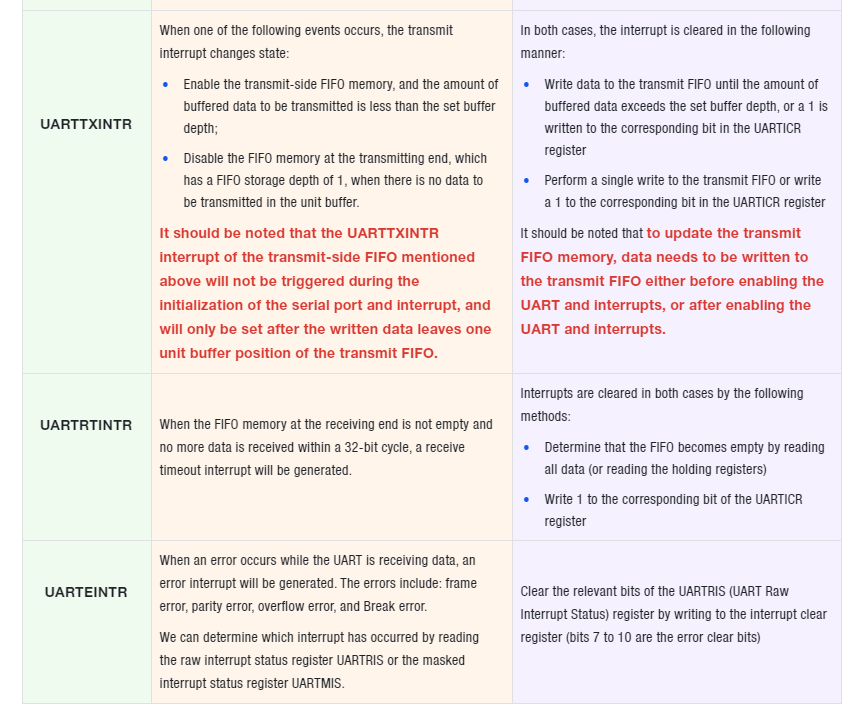
Reception error: A UARTEINTR interrupt is generated, covering the following error conditions:
Frame Error
parity error
Overflow Error
Break error
7.2 Enabling and Disabling UART Interrupts
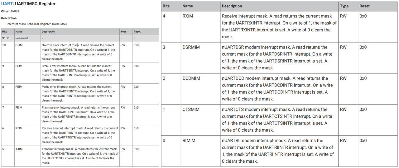
An interrupt event can trigger a controller-level interrupt, and we can enable or disable each individual interrupt by setting or clearing the corresponding bits in the UARTIMSC (Interrupt Mask Set/Clear Register) register:
7.3 Reading of UART Interrupt Status
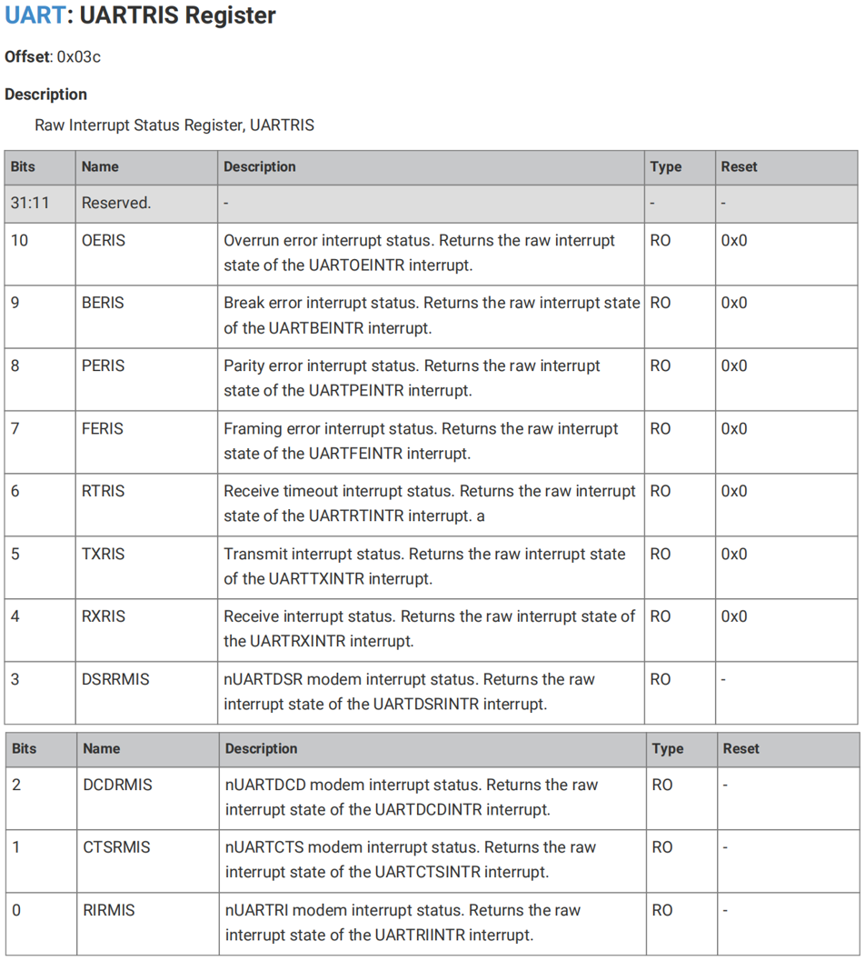
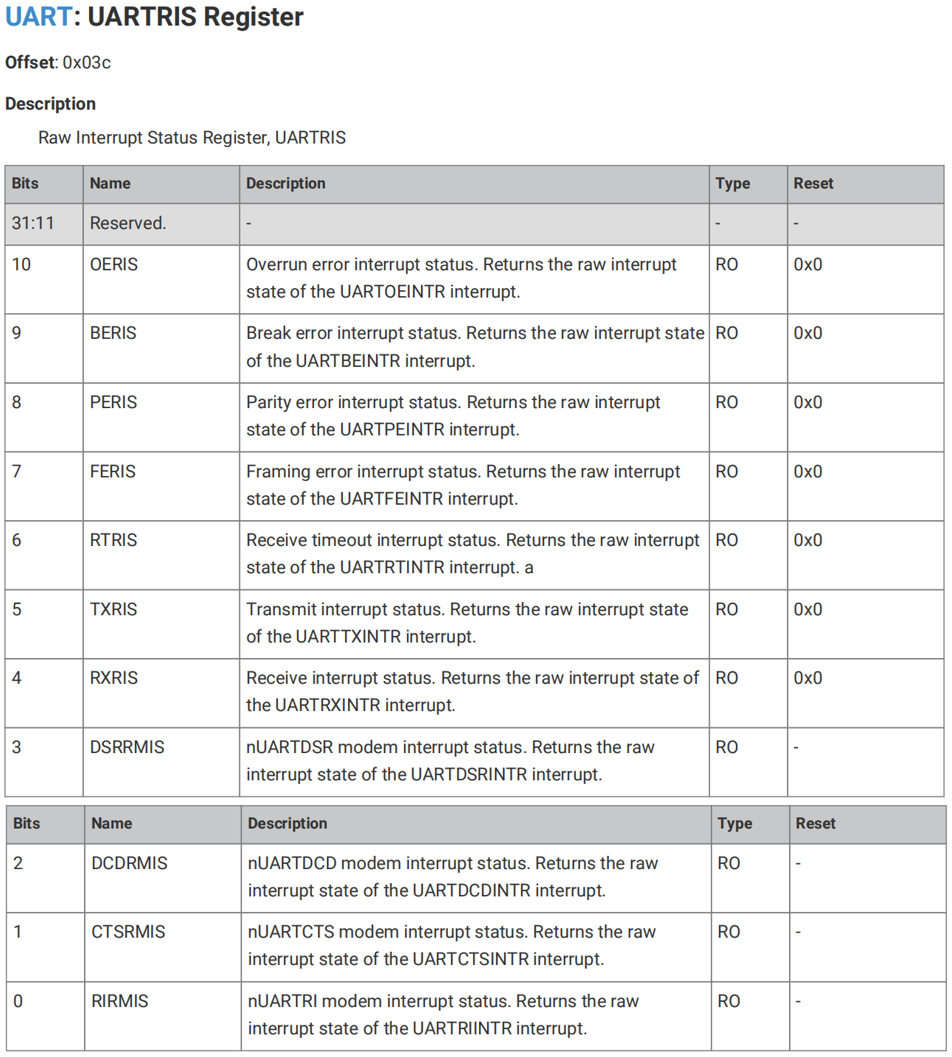
If the interrupt is masked, the status of the source interrupt is always visible through the UART Raw Interrupt Status (UARTRIS) register:
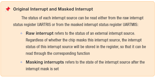
Original Interrupt and Masked Interrupt
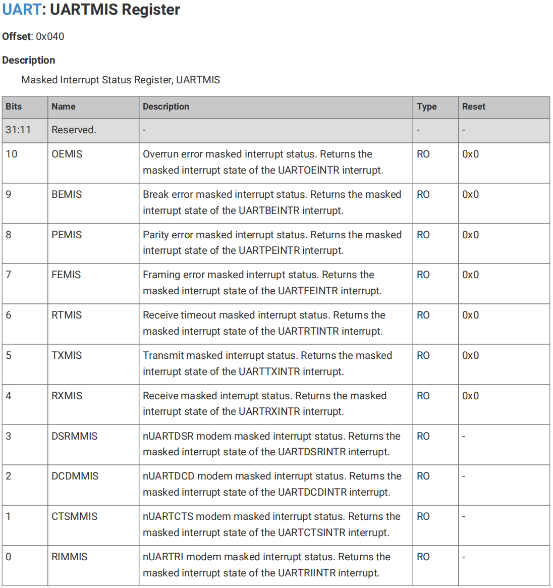
The status of each interrupt source can be read either from the raw interrupt status register UARTRIS or from the masked interrupt status register UARTMIS:
Raw interrupt refers to the status of an external interrupt source. Regardless of whether the chip masks this interrupt source, the interrupt status of this interrupt source will be stored in the register, so that it can be read through the corresponding function
Masking interrupts refers to the state of the interrupt source after the interrupt mask is set
There are 11 maskable interrupts in the UART. After an OR operation, all these 11 interrupts are connected to UARTINTR, which is then linked to the system interrupt controller. The UART can only generate a single interrupt request to the controller at any given time, while software can read the UART Masked Interrupt Status (UARTMIS) register to service multiple interrupt events within a single interrupt service routine:
There are 11 maskable interrupts in the UART. After an OR operation, all these 11 interrupts are connected to UARTINTR, which is then linked to the system interrupt controller. The UART can only generate a single interrupt request to the controller at any given time, while software can read the UART Masked Interrupt Status (UARTMIS) register to service multiple interrupt events within a single interrupt service routine:
7.4 Interrupt Operation of FIFO
The FIFO depth that triggers an interrupt can be controlled via the UART Interrupt FIFO Level Select (UARTIFLS) register, and the two FIFOs can be independently configured to generate interrupts at different threshold levels: