



Raspberry Pi Pico ADC Explained: Hardware, Modes, Registers & Common Pitfalls
In‑depth analysis of RP2040 on‑chip ADC covering hardware architecture, one‑shot /free‑running modes, register description
- ADC Peripheral Introduction
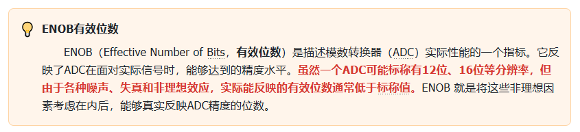
The RP2040 integrates a Successive‑Approximation Register (SAR) ADC. This ADC uses an independent 48 MHz clock and supports a maximum sampling rate of 500 ksps (500 000 samples per second), suitable for medium‑speed signal acquisition. It features 12‑bit resolution, which means it can convert analog input signals into 4096 (2^12) distinct digital values. Its Effective Number Of Bits (ENOB) is 8.7, representing its real‑world practical precision.
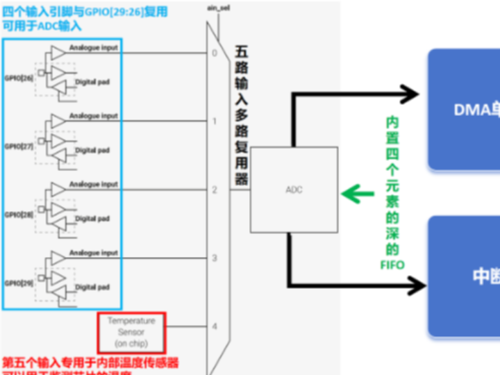
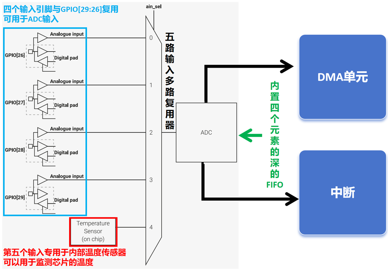
Connection between the on‑chip RP2040 ADC peripheral and GPIO pins:
A digital controller is dedicated to managing ADC operations and provides additional functions:
One‑shot sampling mode or free‑running sampling mode The ADC can be configured to perform a single conversion (one‑shot mode) or run continuous sampling (free‑running capture mode).
Sampling FIFO with DMA interface ADC sampled data is stored inside a FIFO buffer. Data can be transferred to system memory via DMA (Direct Memory Access) to reduce CPU workload.
Ticking timer This timer features 16‑bit integer plus 8‑bit fractional resolution for setting sampling rates under free‑running mode. It allows precise control over sampling time intervals.
Polled multi‑channel sampling Under free‑running mode, the ADC can sample multiple input channels in round‑robin sequence, which is useful when multiple signals need to be acquired simultaneously.
Optional 8‑bit right‑shift output In free‑running mode, sampling results can be optionally right‑shifted to 8‑bit width. Sampled data can then be transferred as bytes via DMA into system‑memory buffers, which helps reduce memory footprint and simplifies byte‑oriented data processing.
When using the ADC peripheral, make sure digital functions of the target pins are disabled. This is accomplished by setting the IE (input enable) bit low (IE = 0) and OD (open‑drain drive) bit high (OD = 1) inside the Pad Control register for that pin.
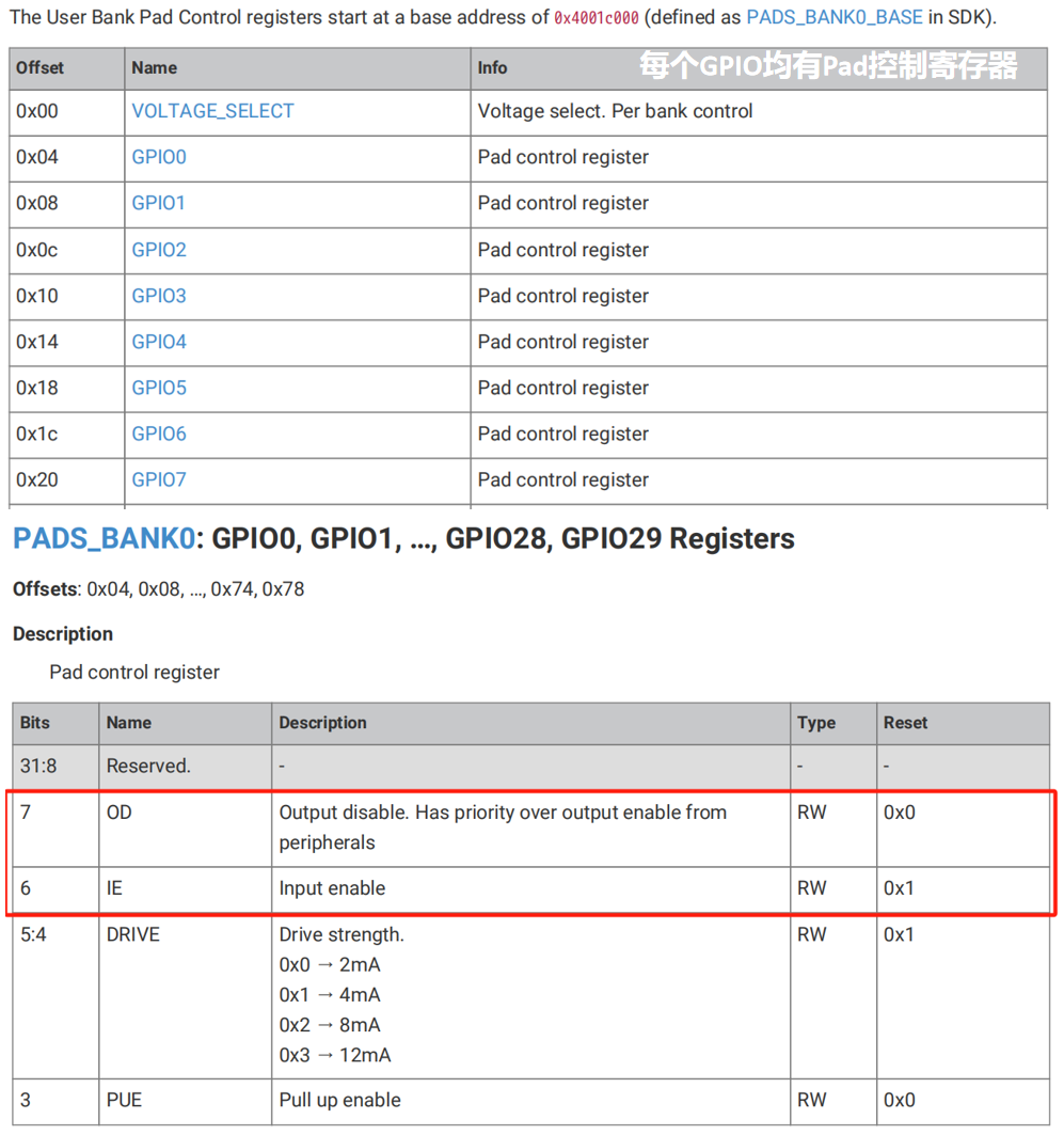
In addition, the maximum allowable ADC input voltage is determined by the digital I/O supply voltage (IOVDD), not the ADC analog supply (ADC_AVDD). For example, if IOVDD equals 1.8 V, ADC input voltage must not exceed 1.8 V even when ADC_AVDD is 3.3 V. Voltages exceeding IOVDD create leakage current through ESD protection diodes and may permanently damage the chip.
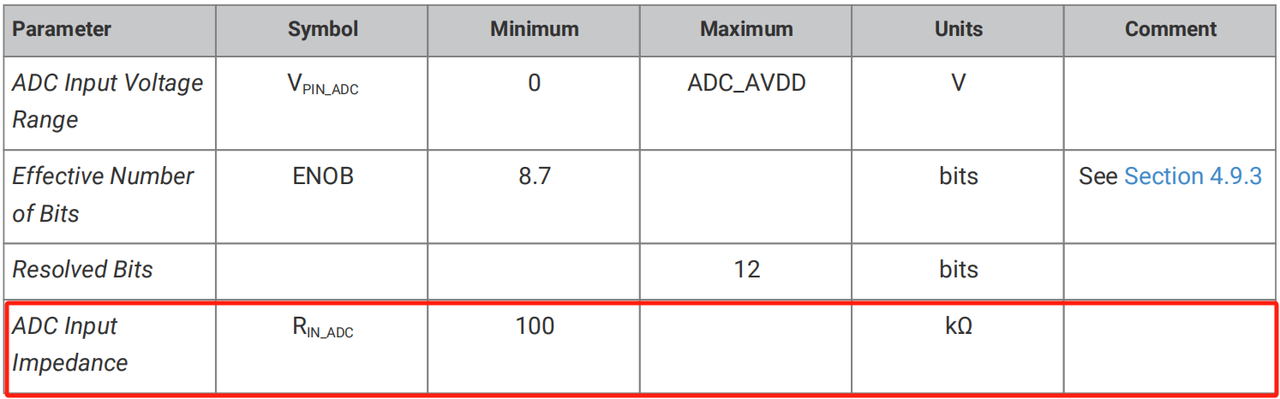
ADC input impedance on Raspberry Pi Pico is approximately 100 kΩ. This impedance value works well for most applications. If the signal‑source impedance is higher than the ADC input impedance, signal attenuation will occur and measurement accuracy will degrade.
As mentioned above, RP2040 integrates a SAR‑type ADC. Its block diagram is shown below:
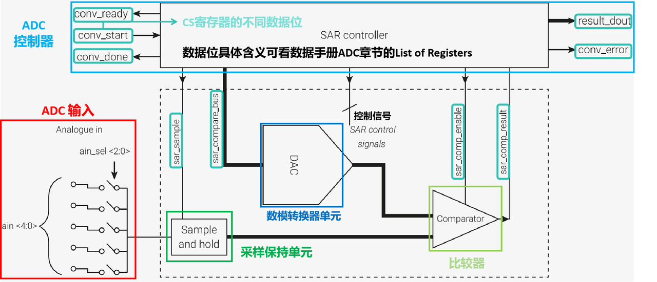
The internal DAC unit inside the SAR ADC is one of its key components. It converts digital values back into analog voltages for comparison against the incoming analog input signal.
The operating sequence of a SAR ADC can be summarised as follows:
- Bit‑by‑bit successive approximation The SAR ADC performs analog‑to‑digital conversion using a successive‑approximation algorithm. It starts from the Most Significant Bit (MSB), sets this bit to logic‑1, then converts this digital setting to an analog voltage via its internal DAC.
- Comparator comparison The generated analog voltage is compared with the incoming analog input signal. If the DAC‑generated voltage is higher than the input signal, the SAR clears this bit; if lower, the bit remains set to 1.
- Continue successive‑approximation process This procedure repeats for every bit position, determining each bit value sequentially until all bits are resolved.
- Final output After completing bit‑by‑bit successive approximation, the resulting digital value represents the digitised version of the original analog‑input signal.
The DAC unit continuously generates different reference voltages and compares them against the input signal to resolve the digital representation of the input. Therefore, DAC precision and linearity are critical metrics for overall SAR‑ADC performance. Inside the RP2040 ADC, this DAC is fully integrated on‑chip; no external DAC chip is required for analog‑to‑digital conversion.
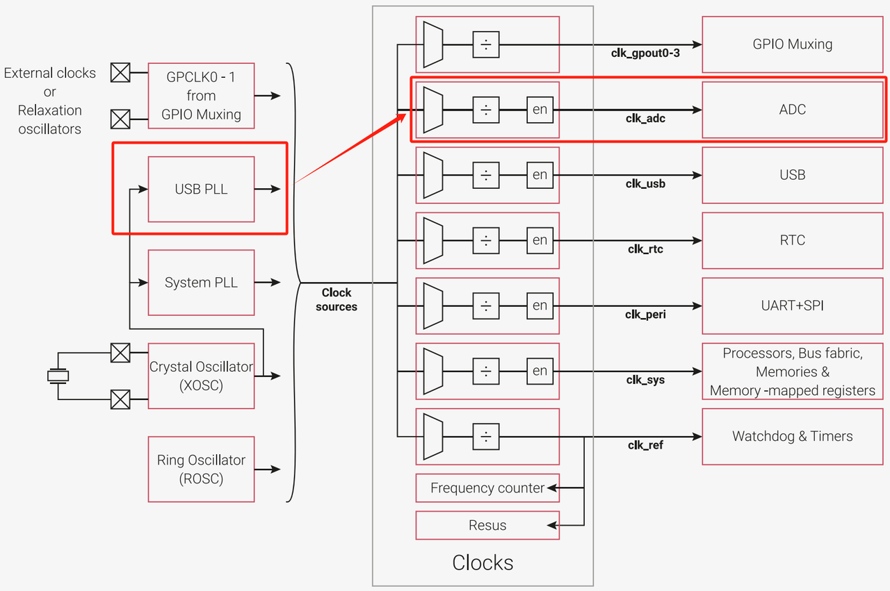
The SAR ADC (Successive‑Approximation Register Analog‑to‑Digital Converter) combines digital‑controller logic and analog circuitry. It requires a 48 MHz clock (clk_adc), which can be sourced from the USB PLL (Phase‑Locked Loop). One sample conversion takes 96 clock cycles: (96 × 1/48 MHz) = 2 µs, corresponding to the 500 ksps maximum sampling rate. The clock must be properly configured before enabling the ADC.
Once the ADC module receives its clock and its reset state is released, setting the EN bit inside the CS control register to 1 triggers a brief internal power‑on sequence for the ADC analog hardware. After several clock cycles, the READY bit inside the CS control register goes high to signal that the ADC is ready for its first conversion.
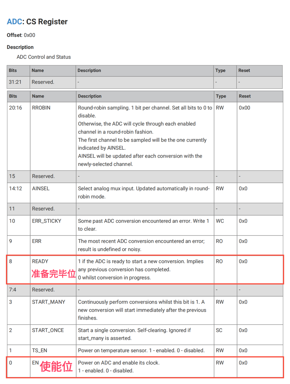
The ADC can be disabled at any time by clearing the EN bit in the CS control register to save power. Note that ADC inputs are capacitive with an on‑chip 1 pF capacitor. At 500 ksps sampling rate its effective input impedance exceeds 100 kΩ. Buffers are generally not required for DC‑voltage measurements.
- ADC Operating Modes
RP2040 ADC supports two operating modes:
One‑shot sampling mode Suitable for on‑demand one‑time analog‑to‑digital conversion events. After triggering a conversion, the ADC completes sampling within 96 clock cycles and returns the result.
Free‑running sampling mode Designed for continuous sampling scenarios such as real‑time data acquisition. After finishing one conversion, the ADC automatically starts the next conversion unless explicit delays are configured.
2.1 One‑shot sampling mode
Under one‑shot mode, writing bit CS.START_ONCE to 1 immediately launches a new analog‑to‑digital conversion. When conversion starts, bit CS.READY goes low to indicate conversion‑in‑progress. After 96 clk_adc clock cycles, CS.READY returns high signalling conversion completion.
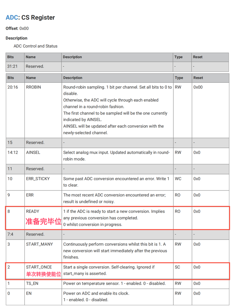
After conversion completes, the 12‑bit conversion result is stored inside the RESULT register.
Prior to starting conversion, select the target ADC input channel by writing to CS.AINSEL. Values 0‑3 select ADC input channels mapped to GPIO 26‑29 respectively; value 4 selects the internal on‑chip temperature sensor.
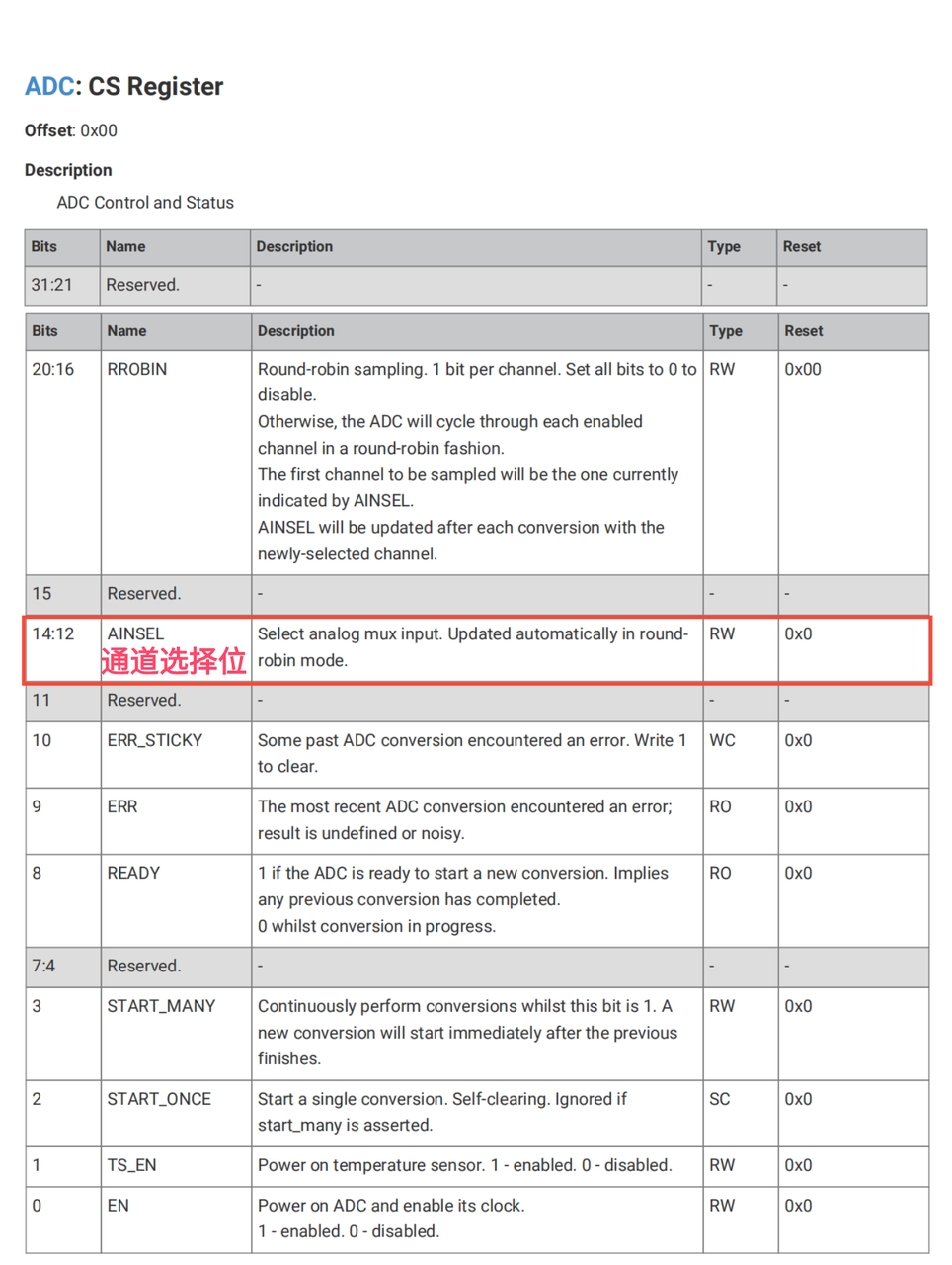
Note: No settling‑time wait is required when switching the AINSEL value. Input channels can be arbitrarily switched just before conversion starts without adversely affecting conversion results.
2.2 Free‑running sampling mode
In free‑running sampling mode, setting bit CS.START_MANY causes the ADC to automatically initiate new conversions at fixed intervals. The most recent conversion result is always held inside the RESULT register. However, when sampled data will be transported using interrupts (IRQ) or DMA, the ADC FIFO must be enabled.
Sampling rate is controlled by configuring the DIV.INT and DIV.FRAC fields within the DIV divider register.
With default setting (DIV = 0), a new conversion begins immediately after the previous conversion finishes, generating one sample every 96 clock cycles. With a 48 MHz clock this yields a sampling rate of 500 ksps.
When DIV.INT is set to a positive integer n, new conversions are triggered every n + 1 clock cycles. Triggers are ignored if a conversion is already running, so n should normally be greater‑or‑equal to 96. As an example, setting DIV.INT = 47999 with a 48 MHz clock results in a 1 ksps sampling rate.
The timer supports fractional‑value frequency division. When DIV.FRAC is non‑zero, new conversions start on average every 1 + INT + FRAC/256 clock cycles. This is achieved by alternating sampling intervals between INT+1 and INT+2 clock cycles.
- Multi‑input sampling
Multi‑input sampling mode is activated by configuring the RROBIN bit‑field inside the CS register. This allows the ADC to automatically switch between different input channels and perform round‑robin sampling under free‑running mode without manual intervention.
Setting a particular bit within CS.RROBIN to 1 enables automatic sampling for the corresponding input channel. Multiple bits set to 1 will make the ADC sample those channels in sequence. If all bits inside CS.RROBIN are zero, round‑robin sampling is disabled and the ADC continuously samples only the channel selected by CS.AINSEL.
Even if the initial AINSEL value is not among channels enabled inside RROBIN, the ADC starts from that current channel and then cycles through channels specified in RROBIN. For instance: initial AINSEL = 0 and RROBIN = 0x06 (bits 1 and 2 set). The sampling‑channel sequence becomes:
- Channel 0
- Channel 1
- Channel 2
- Channel 1
- Channel 2
- Channel 1 …
This round‑robin sequence repeats continuously until CS.RROBIN is disabled.
- Sample‑receive FIFO
Inside the RP2040 ADC module, conversion results can either be read directly from the RESULT register or written into a local receive FIFO buffer, which is read out via the FIFO register.
FIFO behaviour is controlled through the FCS FIFO‑control register.
Definitions for each flag bit:
4.1 FIFO enable and readout
When bit FCS.EN is set to 1, every ADC conversion result gets written into the FIFO. Two consumption methods are available:
‑ Software polls status bits inside the FCS register and reads samples once new data becomes available. ‑ Use interrupts or DMA: read samples from FIFO upon receiving ADC IRQ interrupt or DREQ DMA‑request signals.
4.2 FIFO overflow
When the FIFO is full and another new conversion result arrives, the FCS.OVER error flag bit is asserted. Existing FIFO data is not overwritten; however the newly‑arrived conversion sample is discarded.
4.3 FIFO data‑write formatting
Two bit‑fields inside the FCS register govern data format written to the FIFO:
FCS.SHIFT bit: when set to 1, FIFO data is right‑shifted by 4 bits (bits 7:0 of FIFO correspond to bits 11:4 of conversion result). This facilitates 8‑bit DMA transfers into byte‑wide memory buffers for larger capture buffers at the cost of reduced measurement precision.
FCS.ERR bit: when set to 1, the ERR flag bit for each FIFO entry is asserted, signalling a conversion error. In such cases software should either use the next sample or increase conversion time duration.
Important note: Even when FIFO data is bit‑shifted, the FIFO.ERR flag retains its original bit‑position and correctly indicates conversion‑error status for each individual sample regardless of shifting operations.
These errors indicate that bit‑comparison operations could not complete within the allowed conversion window. This is commonly caused by comparator metastability, which occurs when the analog‑input signal voltage lies very close to comparator threshold levels and requires longer conversion time.
4.4 FIFO combined with DMA usage
The RP2040 DMA controller fetches ADC samples by reading the ADC sample FIFO register, controlled by the ADC_DREQ system data‑request signal. Key points for DMA‑driven ADC data transfers:
- Enable FIFO (
FCS.EN): The FIFO must be enabled so ADC conversion results are written into it. By default the FIFO stays disabled to prevent unintended FIFO filling during one‑shot conversions. - Enable ADC DMA request (
FCS.DREQ_EN): The ADC DREQ signal must be enabled so DMA can perform FIFO reads triggered by ADC data‑request events. - Select
DREQ_ADCas the DMA‑channel data‑request source: The used DMA channel must selectDREQ_ADCas its trigger source for proper synchronisation with ADC events. - Set DREQ assertion threshold (
FCS.THRESH): Set threshold value to 1 so DMA starts transferring as soon as one sample is present inside FIFO. Note that this value also controls IRQ assertion threshold; higher threshold values may be preferred for non‑DMA use‑cases to reduce interrupt frequency. - Configuration for 8‑bit DMA transfers: If DMA transfer width is configured for 8‑bit (transferring into byte arrays in memory),
FCS.SHIFTmust be enabled to pre‑right‑shift samples into byte‑sized values. - Multi‑channel sampling setup: When sampling multiple input channels, configure the 5‑bit mask inside
CS.RROBIN(covering four external input channels plus temperature‑sensor channel). Also setCS.AINSELto select the very first channel for sampling sequence. - Configure ADC sampling rate: Complete ADC sampling‑rate configuration before starting ADC conversions.
After finishing ADC configuration, start the DMA channel first, then trigger ADC conversions by setting the CS.START_MANY bit. Once DMA completes, you may stop the ADC or immediately launch a new DMA transfer. After clearing CS.START_MANY bit to halt the ADC, software must poll CS.READY bit to confirm completion of the final conversion and flush any leftover samples held within FIFO.
4.5 FIFO combined with interrupt usage
Interrupts can be generated whenever sample count stored inside FIFO reaches configurable threshold value FCS.THRESH. Interrupt generation must first be enabled via the FIFO bit‑field within the INTE register.
Interrupt status can be read from the INTS register. Interrupt condition clears when FIFO sample count drops below threshold value defined by FCS.THRESH.
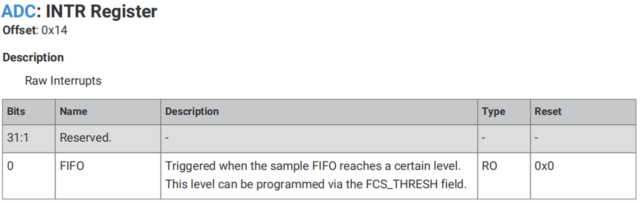
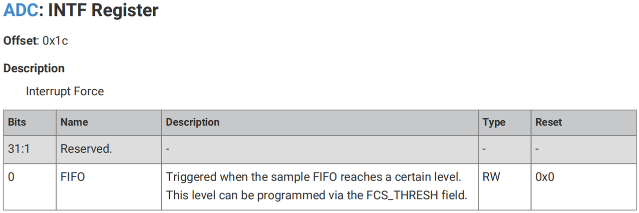
ADC interrupts can be manually forced by writing corresponding bits inside INTF register to 1, without waiting for FIFO sample‑count threshold conditions.
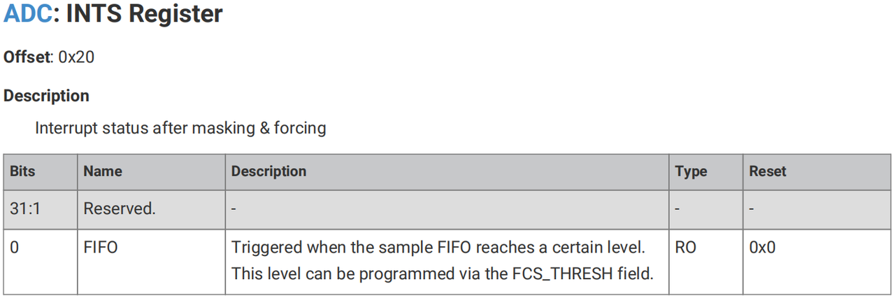
Interrupt masking status and forced‑interrupt events can be inspected through the INTS register.
- ADC effective precision
The RP2040 datasheet documents ADC‑precision characterisation tests, measuring parameters including ENOB (Effective Number of Bits), INL (Integral Non‑Linearity) and DNL (Differential Non‑Linearity). Detailed interpretation is omitted here; readers may refer to official documentation for full details.
- On‑chip temperature sensor
The RP2040 on‑chip temperature sensor measures temperature by reading base‑emitter voltage Vbe of a biased bipolar diode. This sensor is connected to ADC channel 5 (AINSEL = 4). Typically Vbe equals approximately 0.706 V at 27 °C. Temperature‑to‑voltage relationship formula: T = 27 - (ADC_voltage - 0.706) / 0.001721
Where ADC_voltage is the measured base‑emitter voltage. Vbe decreases by roughly 1.721 mV for every 1 °C temperature increase.
Note: The temperature‑sensor reading is highly sensitive to reference‑voltage errors. For example, a 1 % drop in reference voltage (3.3 V → 3.267 V) shifts the temperature reading corresponding to ADC value 891 down to 24.3 °C. Merely 1 % reference‑voltage deviation yields more than 4 °C measurement error. Therefore for improved temperature‑sensor accuracy usage of an external precision voltage reference is recommended.
Before using the temperature sensor, enable its bias‑power supply by setting bit CS.TS_EN. This adds roughly 40 µA current draw on the ADC_AVDD power rail.
RP2040 built‑in temperature sensor is suitable for basic temperature monitoring applications. For high‑precision scenarios reference‑voltage stability must be guaranteed and calibration may be required to compensate for Vbe offset and Vbe temperature‑slope variations.