PIO Underlying Principles Deep‑Dive: Side‑Set to Instruction Execution
RP2040 PIO includes side‑set, wrap, FIFO join, auto‑push/pull, fractional divider and flexible GPIO mapping.
COMPONENTS
PROJECT DESCRIPTION
【Preliminary Note】The original hardware example in this article was written based on the RP2040. The actual hardware used in this hands-on demonstration features the W55RP20 as the main controller chip. The circuit logic and UF2 flashing operation principles are universally applicable, with only the main controller model differing. The original chip model mentioned in the circuit descriptions below is provided for reference purposes only.
Detailed Explanation of PIO Functions and Features
1. Side-set Characteristics
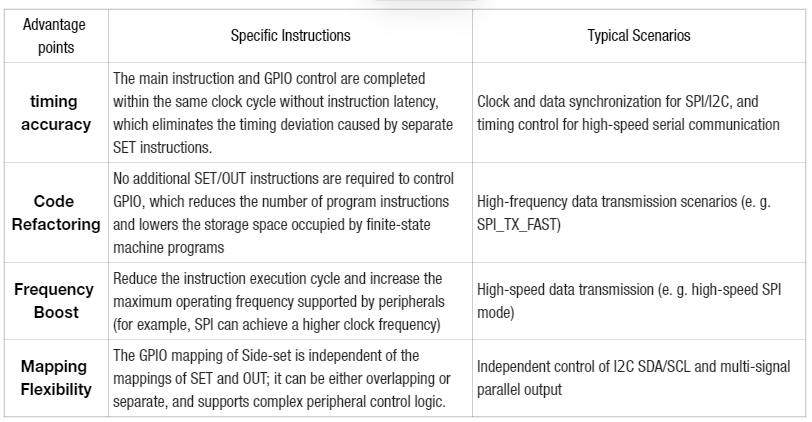
The Side-set feature is designed to simultaneously modify the level (by default) or direction of the specified GPIO while executing the main instruction, enabling parallel execution of the main operation and GPIO control (such as synchronizing "data output" with "clock toggling" in SPI, and synchronizing "data transmission" with "SCL clock" in I2C).
Advantage points
Specific Instructions
Typical Scenarios
timing accuracy
The main instruction and GPIO control are completed within the same clock cycle without instruction latency, which eliminates the timing deviation caused by separate SET instructions.
Clock and data synchronization for SPI/I2C, and timing control for high-speed serial communication
Code Refactoring
No additional SET/OUT instructions are required to control GPIO, which reduces the number of program instructions and lowers the storage space occupied by finite-state machine programs
High-frequency data transmission scenarios (e. g. SPI_TX_FAST)
Frequency Boost
Reduce the instruction execution cycle and increase the maximum operating frequency supported by peripherals (for example, SPI can achieve a higher clock frequency)
High-speed data transmission (e. g. high-speed SPI mode)
Mapping Flexibility
The GPIO mapping of Side-set is independent of the mappings of SET and OUT; it can be either overlapping or separate, and supports complex peripheral control logic.
Independent control of I2C SDA/SCL and multi-signal parallel output
The behavior of Side-set is determined by the underlying hardware mechanism, which is the core difference between it and the SET/OUT instructions, as detailed below:
Coding position: the Delay/side-set field of the instruction to reuse
Each instruction of PIO contains a 16-bit code, where bits 12 to 8 (5 bits) serve as the Delay/side-set field to reuse:
If configured as Delay: this field indicates the number of delay cycles (0~31) after the instruction is executed;
If configured as Side-set: this field indicates the side-set data to be written to GPIO (ranging from 0 to 31, corresponding to a maximum of 5 GPIO pins);
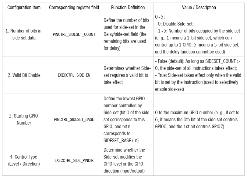
Field allocation is controlled by PINCTRL_SIDESET_COUNT: if set to 1, it occupies 1 bit, leaving 4 bits available for delay; if set to 5, all 5 bits are used for sideset and no delay function is available.
Pin Mapping: Independent of SET/OUT, supports overlapping
Side-set has a dedicated GPIO mapping configuration (PINCTRL_SIDESET_BASE) that specifies the starting GPIO number for sideset control, which is independent of PINCTRL_SET_BASE for SET and PINCTRL_OUT_BASE for OUT;
The GPIO mapping of side-set can overlap with the mapping of SET/OUT (for example, the same GPIO is used by OUT for data output and by side-set for clock control at the same time). In this case, side-set has a higher priority than SET/OUT (if written simultaneously, the data from side-set shall prevail).
Effective Timing: Takes effect immediately, independent of the instruction pending status
Regardless of whether the main instruction enters a waiting state (for example, the PULL instruction waits for TX FIFO data, and the PUSH instruction waits for RX FIFO space), the side-set data takes effect immediately in the first clock cycle of instruction execution;
This ensures that the timing of GPIO control will not be delayed by the waiting of main instructions, which is the key to timing stability in high-speed communication.
Compatibility: All PIO instructions are supported, and any PIO instruction (such as OUT, IN, JMP, MOV, SET, PULL, PUSH, etc.) can be used in combination with Side-set. The side-set data is specified via the side <value> identifier that follows the instruction.
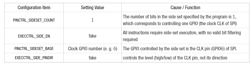
To use Side-set, you need to set 4 key options via the PIO configuration register to determine the bit width, activation rule, GPIO mapping and control type of the side-set, as detailed below:
The following is a line-by-line breakdown of the spi_tx_fast program, combined with configuration instructions for the practical use of Side-set:
.program spi_tx_fast ; 定义了一个名为 spi_tx_fast 的程序
.side_set 1 ; 设置侧集数据位数为1

loop:
    out pins, 1 side 0 ;将1个数据位传输到GPIO引脚1上,同时使用Side-set操作设置将其设置为低电平
    jmp loop side 1 ; 这行指令跳转回 loop 标签,同时 Side-set 操作设置将其设置为高电平
Combined with the program's. side_set 1, the 4 configuration items of this example are set as follows:
配置项
设置值
原因 / 作用
PINCTRL_SIDESET_COUNT
1
程序指定侧集位数为 1,对应控制 1 个 GPIO(SPI 的时钟 CLK)
EXECCTRL_SIDE_EN
假
所有指令都需要执行 Side-set,无需有效位筛选
PINCTRL_SIDESET_BASE
时钟 GPIO 编号(如 6)
侧集控制的 GPIO 为 SPI 的 CLK 引脚(GPIO6)
EXECCTRL_SIDE_PINDIR
假
控制的是 CLK 引脚的电平(高 / 低),而非方向
spi_tx_fast Example:
Execution Timing: Each instruction occupies 1 system clock cycle. out pins, 1 side 0 When executed, data output is completed synchronously with the CLK going low. jmp loop side 1 When executed, the jump is completed synchronously with the CLK going high. The entire loop takes only 2 clock cycles to output 1 bit of SPI data, enabling high-frequency data transmission.
Advantages: No additional SET instructions are required to control the CLK pin, which simplifies the code; data and clock are executed synchronously with no timing deviation, significantly boosting the maximum SPI frequency.
spi_tx_fast This example demonstrates two advantages of side-set: more precise alignment between data and clock, faster overall program execution — in this case, one data bit can be output every two system clock cycles — and a smaller program size.
In I2C communication, the GPIO mapping division of labor for Side-set, OUT, and SET is as follows, which reflects the flexibility of side-set:
Side-set: The SCL clock pin of I2C, which is responsible for clock toggling and synchronizing data transmission;
OUT: SDA data pin of I2C (responsible for shifting out data bits);
SET: I2C SDA data pin (responsible for generating pulses of special sequences such as Start/Stop); through this mapping division of labor, the finite-state machine can flexibly control the data output or special pulses of SDA while SCL provides the clock, and SDA/SCL can be mapped to any GPIO without being restricted by hardware pins.
Please note the following during use:
Resource contention between Delay and Side-set: The Delay/side-set field is to reuse. The more bits occupied by the side-set, the fewer bits available for delay (for example, if the side-set occupies 5 bits, the delay function cannot be used; if it occupies 1 bit, the maximum delay is 15 (4 bits)).
Priority Rule: If Side-set and SET/OUT write to the same GPIO at the same time, the data of Side-set will overwrite the data of SET/OUT. Therefore, the GPIO mapping shall be reasonably planned according to the business scenario.
Usage scenarios of valid bits: When EXECCTRL_SIDE_EN is set to true, only the Side-set of some instructions takes effect, which is applicable to scenarios requiring selective GPIO control (e. g., toggling the clock only during data transmission and performing no operation when idle).
Usage of Direction Control: When EXECCTRL_SIDE_PINDIR is set to true, the Side-set modifies the GPIO direction, which is applicable to scenarios requiring dynamic switching of GPIO input/output (such as bidirectional communication on the SDA pin of I2C).
2. Program Reentry
Program Wrap is a hardware-level looping mechanism for the PIO finite-state machine, which essentially configures dedicated registers (EXECCTRL_WRAP_BOTTOM and EXECCTRL_WRAP_TOP) to make the program counter (PC) automatically jump to the preset start address (WRAP_BOTTOM) when it reaches the specified address (WRAP_TOP), instead of executing a software-level JMP jump instruction.This feature specifically addresses the issues of instruction memory occupancy and execution cycle overhead caused by traditional JMP loops, and serves as a core hardware optimization method to improve the execution efficiency of PIO programs and save instruction memory.
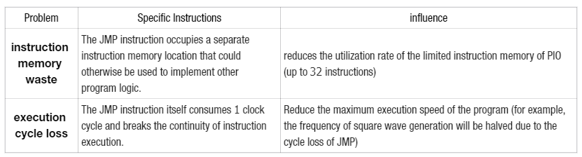
If a PIO program uses the JMP instruction to implement outer loops (such as the repetitive steps of square wave generation or data transmission), it will have the following two notable drawbacks, which are also the core pain points that the program looping-back feature is designed to address:
问题点
具体说明
影响
指令内存浪费
JMP 指令需要占用 1 个独立的指令内存位置,而该位置本可用于实现其他程序逻辑
减少了 PIO 有限的指令内存(最多 32 条指令)的利用率
执行周期损耗
JMP 指令本身需要消耗 1 个时钟周期,且会打破指令执行的连续性
降低程序的最大执行速度(如方波生成的频率会因 JMP 的周期损耗减半)
Taking the output of a square wave signal as an example, the code is as follows:
.program squarewave
    set pindirs, 1 ; 步骤1:设置引脚为输出模式(1个周期)
again:
    set pins, 1 [1] ; 步骤2:引脚置高,延时1周期(共2个周期:指令1个+延时1个)
    set pins, 0 ; 步骤3:引脚置低(1个周期)
    jmp again ; 步骤4:跳转回again(1个周期)
This code implements a simple square wave signal generator. It generates a square wave signal by switching between high and low levels with an added delay. jmp jump instruction itself takes one cycle, and each set instruction also takes one cycle, so to ensure that the high and low level signals are maintained for the same duration, the set pins, 1 instruction adds a one-cycle delay, making the finite-state machine wait for one cycle before executing the set pins, 0 instruction. Each loop takes a total of 4 cycles.
Here, there are two issues:
JMP occupies instruction memory that could otherwise be allocated to other programs
The additional cycles required to execute JMP reduce the maximum output speed by half.
Since the program counter (PC) will automatically wrap around to 0 when it exceeds 31, filling the entire instruction memory with set pins, 1 and set pins, 0 can solve the second problem, but this approach wastes a significant amount of memory.
The PIO assembler (pioasm) provides two dedicated assembler directives to mark the start and end positions of the loopback, which will eventually be mapped to the hardware register (EXECCTRL control register), thus solving both problems:
The above code can remove the delay cycle, so that the output speed will be twice as fast as before, while maintaining an equal duration for both the high level and low level:
Execute set pins, 1 [1](PC= 1), and increment PC by 1 to PC= 2 upon completion;
Execute set pins, 0 [1](PC= 2), upon completion, PC will be equal to WRAP_TOP (2), and automatically jump to WRAP_BOTTOM (1) instead of incrementing PC by 1;
After executing an instruction in the program memory, the state machine updates the program counter using the following logic PC:
If the current instruction is JMP, and Condition is true, then set PC to Target
Otherwise, if PC is equal to EXECCTRL_WRAP_TOP, set PC to EXECCTRL_WRAP_BOTTOM
Otherwise, PC increments by 1; however, if the current value is 31, it will be set to 0
pioasm. wrap_target and. wrap assembler directives are effectively labels; they export constants that are written to WRAP_BOTTOM and WRAP_TOP respectively.
The sample code above, processed by the PIO assembler pioasm and compiled, will generate the following files:
As we can see, the PIO assembler (pioasm) will convert. wrap_target and. wrap into constants and generate the corresponding configuration functions, specifically including:
Define xxx_wrap_target and xxx_wrap macros to store the return relative address;
Generate the pio_program structure, which contains information such as the instruction sequence and its length.
Generate xxx_program_get_default_config function, which automatically writes the wrap address to pio_sm_config (by calling the sm_config_set_wrap function).
When using the program loopback feature, the following points should be noted:
Absoluteness of Addresses: WRAP_BOTTOM and WRAP_TOP are absolute addresses of PIO instruction memory, not relative addresses;
Offset adjustment: If the program is loaded to a non-zero offset position in the instruction memory (e. g., offset= 5), the returned relative address shall be added with the offset to obtain the absolute address before being written into the register;
Direct register configuration: If the default configuration function is not used, you can directly use the pio_sm_set_wrap function or modify the EXECCTRL register's WRAP_BOTTOM / WRAP_TOP fields to configure the wrap address.
It should also be noted that:
Range restriction for wrap-around addresses: WRAP_BOTTOM must be less than or equal to WRAP_TOP, and neither of them shall exceed the maximum address (31) of the PIO instruction memory; otherwise, the wrap-around logic will fail.
Compatibility with JMP Instructions: The program loopback mechanism does not affect the execution of JMP instructions (as JMP has a higher priority), so JMP can be used inside a loopback loop to implement conditional branches, balancing loop efficiency and logical flexibility.
Priority of natural wrap-around: If program wrap-around is not configured (WRAP_BOTTOM = 0 and WRAP_TOP = 31), the PC will automatically reset to 0 when it reaches 31. This is the natural wrap-around feature of the PIO instruction memory, which can be regarded as the default case of program wrap-around.
Compatibility of Delay and Side Set: The wrap-around logic only affects the update of the PC, and will not affect the delay ([n]) or side set (side n) features; both the delay and side set will still take effect normally.
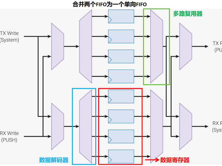
3. FIFO Merge
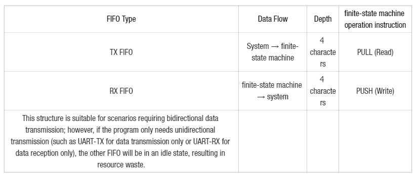
The default FIFO for each PIO finite-state machine is "bidirectional double buffer":
However, many programs do not require bidirectional data transfer between the system and the finite-state machine, but a longer FIFO is quite useful, especially in high-bandwidth interfaces such as DPI image transmission. In these cases, you can use the SHIFTCTRL_FJOIN option to combine two 4-word-long FIFOs into one 8-word-long FIFO.
The essence of FIFO merging is to integrate two 4-word FIFO resources into one 8-word unidirectional FIFO, which has two core values:
Increase FIFO depth: Increasing the depth from 4 words to 8 words allows more data to be temporarily stored, thus reducing the system interrupt frequency (for example, during UART reception, the deeper the FIFO, the less frequently interrupts need to be triggered to fetch data);
Avoid resource waste: In unidirectional transmission scenarios, idle FIFO resources can be fully utilized (for example, when only the TX finite-state machine is used, the RX FIFO can also be converted to a TX FIFO).
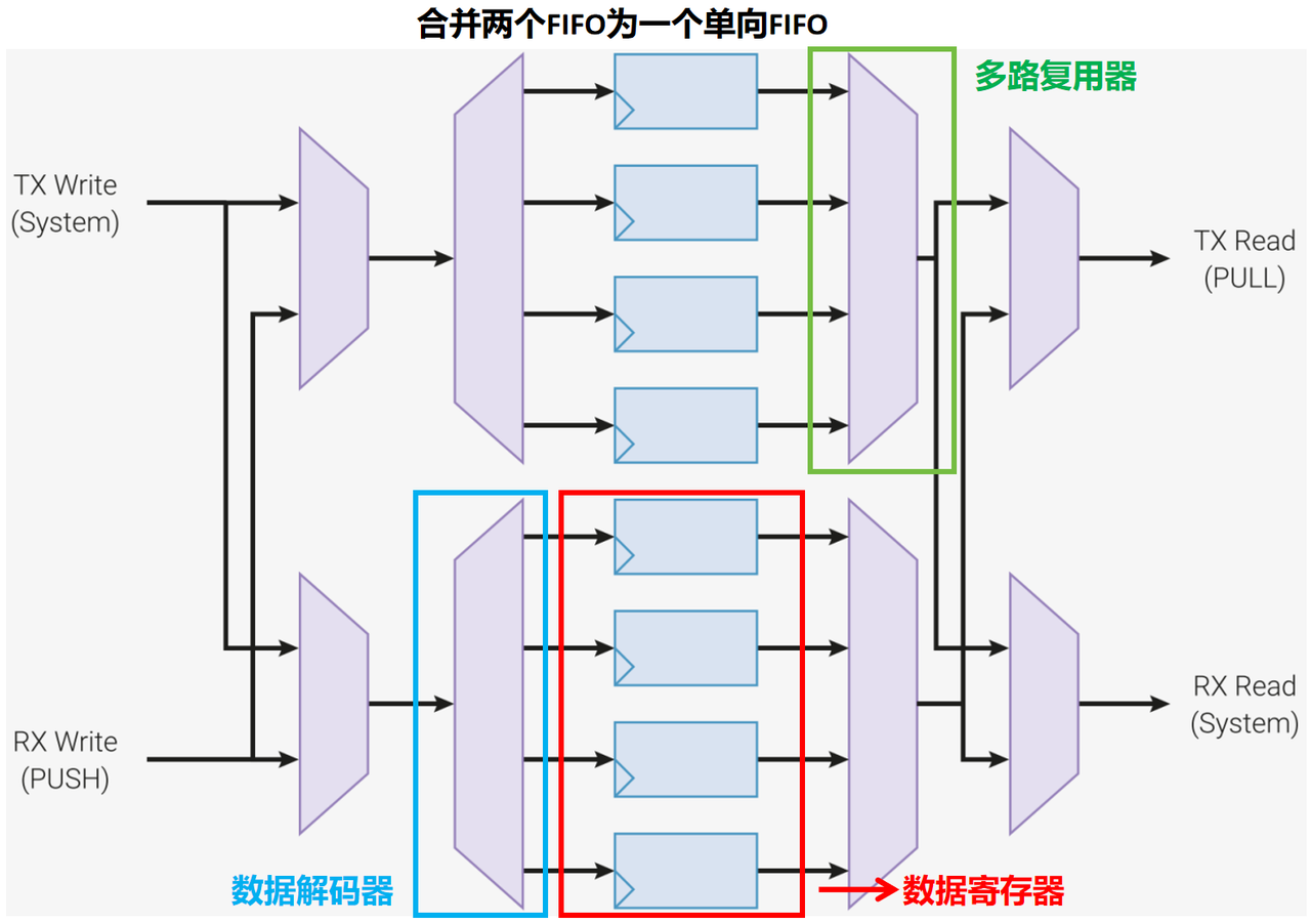
The hardware structure of FIFO merging consists of a data decoder and a multiplexer (corresponding to the diagram you provided titled "Merge Two FIFOs into a Unidirectional FIFO"), and its working process is as follows:
Data Writing: When the system writes data to the FIFO via "TX Write" or "RX Write", the data decoder will allocate the data to the corresponding original FIFO (the original TX FIFO or original RX FIFO);
Data Read: The merged FIFO passes through a multiplexer, which "merges" the data from the original TX FIFO and original RX FIFO into a single data stream for the finite-state machine to PULL read (when merged as a TX FIFO), or for the system to read (when merged as an RX FIFO);
Unidirectional to reuse: After merging, only the "full TX" or "full RX" mode can be selected. At this point, the FIFO resource in the other direction will be to reused as the buffer for the current direction, ultimately forming an 8-word unidirectional FIFO.
The combined FIFO provides a 1:4 data decoder and a 4:1 multiplexer, enabling us to perform write and read operations between the TX and RX channels of the FIFO, so that all 32-bit × 8-word data can be accessed from both ports.
UART is a typical scenario of "unidirectional finite-state machine implementation", where independent finite-state machines are used for TX and RX respectively:
Default case: The TX finite-state machine uses its own 4-word TX FIFO, the RX finite-state machine uses its own 4-word RX FIFO, and the other FIFO of both sides is idle;
After merging:
The TX finite-state machine can combine its own TX+ RX FIFO into an 8-word TX FIFO, which can temporarily store more data to be transmitted and reduce the number of interrupts generated by the system writing to the FIFO;
The RX finite-state machine can merge its own RX+ TX FIFO into an 8-word RX FIFO, which can temporarily store more received data and eliminates the need for the system to frequently interrupt to fetch data; ultimately, the UART with an 8-word FIFO processes interrupts at only half the frequency of that with a 4-word FIFO, improving system efficiency.
After merging the FIFOs, the FIFO of the finite-state machine will become a structure of "unidirectional 8 words + 0 words", and the corresponding states and instruction behaviors will change:
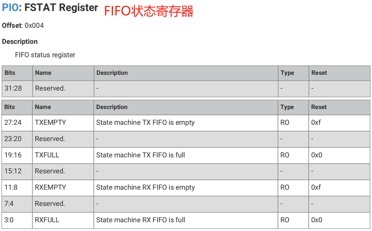
FIFO Status: The FIFO status is indicated by the FSTAT register (the second figure you provided). When merged, the "unused FIFO" will be in both the full (FULL) and empty (EMPTY) states simultaneously:
If combined into TX FIFO (8 words):
TX FIFO works normally, FSTAT. TXEMPTY / TXFULL indicates the actual status;
RX FIFO is disabled, FSTAT. RXEMPTY and RXFULL will be set to 1 simultaneously (indicating that the RX FIFO is both full and empty and cannot be used);
If merged into RX FIFO (8 words):
RX FIFO operates normally, FSTAT. RXEMPTY / RXFULL indicates the actual status;
When the TX FIFO is disabled, FSTAT. TXEMPTY and TXFULL will be set to 1 simultaneously.
Impacts of finite-state machine instructions: After merging, the instructions corresponding to the disabled FIFO will fall into a permanent waiting state:
When merged into TX FIFO: the finite-state machine executes the PUSH instruction (writing data to the RX FIFO) and keeps waiting (since the depth of the RX FIFO is 0, no data can be written);
When merged into RX FIFO: the finite-state machine executes the PULL instruction (to read data from the TX FIFO) and will keep waiting (since the depth of the TX FIFO is 0, there is no data available to read).
It should be noted that when merging FIFOs or separating merged FIFOs, all data in the FIFO of the current finite-state machine will be discarded. If the data cannot be recovered, the FIFO queue must be emptied in advance.
An 8-word deep FIFO is sufficient to work with the DMA of the RP2040 to achieve the high transfer rate of "1 byte per clock cycle", provided that the DMA is not blocked by other tasks.
4. Auto-ejection and Auto-loading
First, let's review the "shift and data padding" logic of the two core registers:
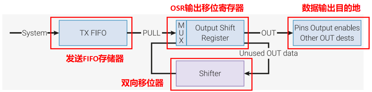
OSR (Output Shift Register): The finite-state machine shifts out data via the OUT instruction. After the data is shifted out, the OSR will become "empty", and new data needs to be supplemented from the TX FIFO (the buffer from the system to the finite-state machine)(manually using the PULL instruction);
ISR (Input Shift Register): The finite-state machine shifts data in via the IN instruction; once the data is shifted in, the ISR will become "full", and the data needs to be pushed to the RX FIFO (the buffer from the finite-state machine to the system)(manually via the PUSH instruction).
The core of automatic push/loading is to let the hardware automatically complete the operations of "supplementing OSR data" and "pushing ISR data", without the need to manually write PULL/PUSH instructions, which not only saves instruction memory but also improves data transmission efficiency.
First, let's look at a sample program for manually loading OSR data and analyze its flaws:
.program manual_pull
.side_set 1 opt ; 设置 Side-set 侧集操作位数为1,opt 以指定 side <value> 对于指令是可选的

.wrap_target ; 标记了 .wrap 指令的目标位置
    set x, 2 ; 将寄存器 x 初始化为 2,这个寄存器会用于控制循环次数
    pull side 1 [1] ; 执行手动拉取操作,如果没有 TX 数据,则会在这里等待
bitloop: ; 这里定义了一个标签,用于循环输出数据位
    out pins, 1 side 0 [1] ; 将 1 位数据移位输出到 GPIO 引脚,同时将 Side-set 设置为 0,用于控制时钟
    jmp x-- bitloop side 1 [1] ; 递减寄存器 x,如果不为 0,则跳转回 bitloop 标签
    out pins, 1 side 0 ; 输出最后一位数据,Side-set 设置为 0
.wrap ; 无条件跳转回 .wrap_target 标记的位置
The program shifts 4 data bits out of each FIFO word at a rate of 1 data bit transmitted every 4 clock cycles, while outputting a clock signal. When the TX FIFO is empty, the program pauses at the high level of the clock.(Note that the side-set remains active during the cycle when the instruction is paused.)
This program has a number of limitations:
High instruction slot occupancy: only 2 out of 5 instruction slots are used for actual data output, while the rest are reserved for counter initialization, manual PULL operations and jumps;
Low throughput: Only 1 bit of data can be shifted out every 4 system clock cycles, and the speed is limited by the cycle loss of manual instructions;
Poor flexibility: The number of bits to be shifted out is fixed (depending on the X counter), so it cannot dynamically adapt to different data lengths.
At this point, we can enable the autopush function for automatic data push and the autopull function for automatic data loading:
The core of automatic loading is: the "shift counter" of the hardware tracking OSR. When the number of shifted-out bits reaches the configured threshold, data is automatically loaded from the TX FIFO to the OSR without manual PULL;
The logic of automatic push is symmetrical to that of automatic loading: the hardware tracks the "shift counter" of the ISR, and when the number of shifted-in bits reaches the configured threshold, it automatically pushes the ISR data to the RX FIFO without manual PUSH.
When autopush data auto-push is enabled, the finite-state machine will automatically execute the IN instruction to load data from the ISR register and push it to the RX FIFO once the count threshold of the set shift counter is reached, and meanwhile clear the corresponding data in the ISR register:
The finite-state machine executes OUT instruction, and the OSR shift counter accumulates the number of bits shifted out;
When the counter reaches SHIFTCTRL_PULL_THRESH (the configured threshold), hardware automatically triggers PULL;
Read one 32-bit data from the TX FIFO (transmit FIFO memory) and load it into the OSR output shift register;
The OSR shift counter is cleared and waits for the next round of shifting out.
After enabling automatic rollout, the code is as follows:
.program autopull
.side_set 1 ; 侧集位数1

.wrap_target
    out pins, 1 side 0 [1] ; 移出1位数据,侧集时钟置0
    nop side 1 [1] ; 空操作,侧集时钟置1(替代手动跳转)
.wrap
Advantages of this program:
Streamlined instruction set: only 2 instructions, with no counter or jump logic;
2x speedup: eliminates the periodic overhead caused by manual PULL/jump; if latency is removed, the throughput can reach "1 bit shifted out per 2 system clock cycles";
High flexibility: The number of bits to be shifted is controlled by the hardware threshold (rather than code), and can be dynamically configured as 16/32 bits.
Enable the autopull automatic data loading function. When the count threshold of the set shift counter is reached, the finite-state machine will automatically execute the OUT instruction to load data from the FIFO. Enabling automatic data loading can save the time required for manually executing the OUT instruction and achieve higher data throughput compared with manual execution of the OUT instruction:
The finite-state machine executes IN instruction, and the ISR shift counter accumulates the number of bits shifted in;
When the counter reaches SHIFTCTRL_PUSH_THRESH (the configured threshold), hardware automatically triggers PUSH;
The 32-bit data of the ISR input shift register is pushed into the RX FIFO (receive FIFO memory);
The ISR shift counter is cleared and waiting for the next round of shifting-in.
Using the autopull function, manual_pull the example can be rewritten as follows:
.program autopull
.side_set 1

.wrap_target
    out pins, 1    side 0      [1]
    nop            side 1      [1]
.wrap
This program is shorter and simpler than the original version, and runs twice as fast if the delay is removed, since automatically loading the OSR via hardware does not consume clock cycles during instruction execution. Note that the program does not know how many data bits need to be shifted before the next load; the hardware will automatically load once the configured threshold (SHIFTCTRL_PULL_THRESH) is reached, so the example program can also shift out 16 or 32 data bits from each FIFO word.
Finally, note that the above program is not completely identical to the original one: it will pause when the clock signal (note that this is not the system clock, but the communication clock) is low, rather than when it is high. This behavior is mainly caused by the design feature of the PIO finite-state machine, which executes instructions based on clock pulse edges. In the out pins, 1 side 0 [1]instruction, data output occurs on the falling edge of the clock signal, while the nop side 1 [1]instruction is executed on the rising edge of the clock signal.Therefore, when the TX FIFO is empty, the finite-state machine will pause during the low level phase of the clock signal and resume execution only after new data enters the TX FIFO.
We can adjust the pause position via the PULL IFEMPTY instruction, which adopts the same configurable threshold as autopull; after using this instruction, it can simplify certain programs to control where the pause occurs just like autopull does. When both OSR and TX FIFO are empty, the finite-state machine will enter the pause state upon executing OUT.
.program somewhat_manual_pull
.side_set 1

.wrap_target
    out pins, 1    side 0      [1]
    pull ifempty   side 1      [1]
.wrap
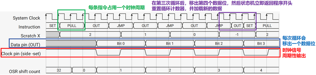
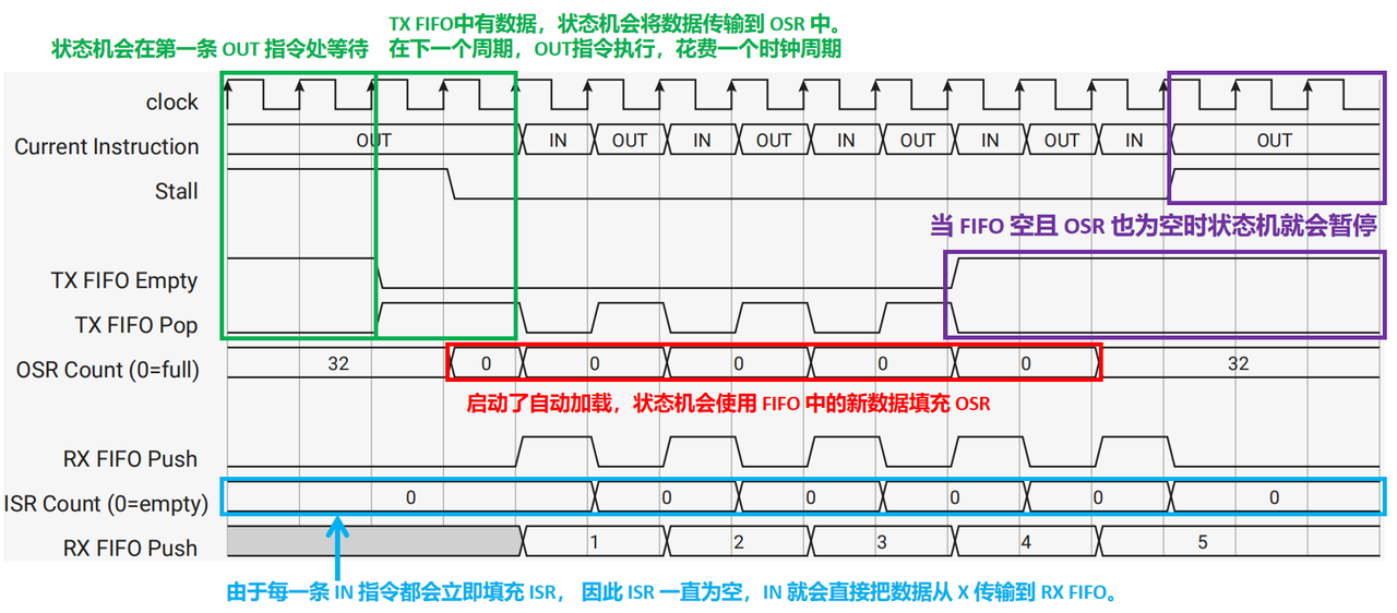
The following is a complete example, including a PIO program and a C program that loads and runs it, demonstrating how to enable both autopull and autopush simultaneously on the same finite-state machine. The function of finite-state machine 0 is to transfer data from the TX FIFO to the RX FIFO, with a throughput of one byte every two clock cycles.
The PIO program is as follows:
.program auto_push_pull ; 定义了一个名为 auto_push_pull 的程序

.wrap_target
    out x, 32 ; 将 32 位数据从寄存器 x 自动推送(auto-push)到 TX FIFO
    in x, 32 ; 从 RX FIFO 自动拉取(auto-pull) 32 位数据到寄存器 x
.wrap
A C program for loading and running PIO programs
#include "tb.h" // TODO this is built against existing sw tree, so that we get printf etc

#include "platform.h"
#include "pio_regs.h"
#include "system.h"
#include "hardware.h"

#include "auto_push_pull.pio.h"

int main()
{
    // 用于初始化测试环境
    tb_init();

    // 加载并配置 PIO 状态机 0 来运行 auto_push_pull 程序
    // 将 auto_push_pull_program 数组中的指令加载到 PIO 指令存储器中
    for (int i = 0; i < count_of(auto_push_pull_program); ++i)
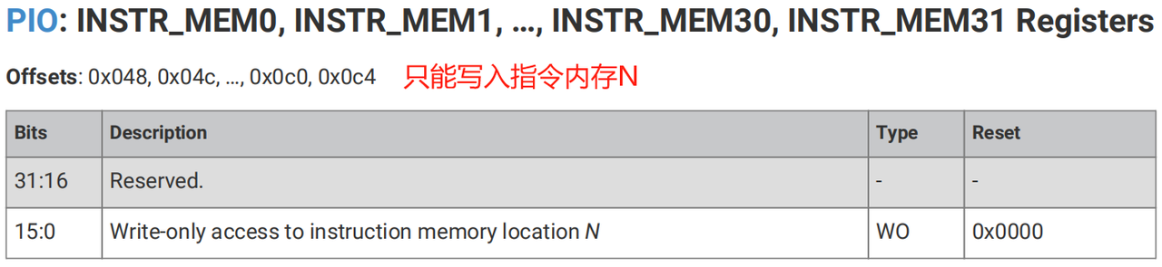
        mm_pio->instr_mem[i] = auto_push_pull_program[i];

    // 配置状态机 0 的 SHIFTCTRL 寄存器
    // 启用自动推送和自动拉取功能,设置推送和拉取阈值为 32
    mm_pio->sm[0].shiftctrl =
            (1u << PIO_SM0_SHIFTCTRL_AUTOPUSH_LSB) |
            (1u << PIO_SM0_SHIFTCTRL_AUTOPULL_LSB) |
            (0u << PIO_SM0_SHIFTCTRL_PUSH_THRESH_LSB) |
            (0u << PIO_SM0_SHIFTCTRL_PULL_THRESH_LSB);

    // 配置状态机 0 的 EXECCTRL 寄存器,设置 .wrap_target 和 .wrap 指令的位置
    mm_pio->sm[0].execctrl =
            (auto_push_pull_wrap_target << PIO_SM0_EXECCTRL_WRAP_BOTTOM_LSB) |
            (auto_push_pull_wrap << PIO_SM0_EXECCTRL_WRAP_TOP_LSB);

    // 启动状态机 0
    hw_set_bits(&mm_pio->ctrl, 1u << (PIO_CTRL_SM_ENABLE_LSB + 0));

    // 向 TX FIFO 中写入 5 个数据,并从 RX FIFO 中读取并打印出 5 个数据
    for (int i = 0; i < 5; ++i)
        mm_pio->txf[0] = i;
    for (int i = 0; i < 5; ++i)
        printf("%d\n", mm_pio->rxf[0]);

    return 0;
}
The following figure illustrates the entire execution flow of the finite-state machine:
To trigger automatic push or automatic load at the correct time, the finite-state machine uses a pair of 6-bit shift counters to track the total number of shifts for the ISR and OSR respectively:
After a reset, or when CTRL_SM_RESTART is triggered, the ISR shift counter is set to 0 (no data has been shifted in yet), and the OSR shift counter is set to 32 (no data is pending to be shifted out);
OUT instruction increments the OSR shift counter by Bit count;
IN instruction increments the ISR shift counter by Bit count;
PULL instruction or automatic loading will clear the OSR counter to 0;
The PUSH instruction or an automatic pop operation will clear the ISR counter to 0;
MOV OSR, x or MOV ISR, x will clear the OSR or ISR shift counter to 0;
OUT ISR, n instruction sets the ISR shift counter to n.
When executing any OUT or IN instruction, the finite-state machine compares the shift counter against SHIFTCTRL_PULL_THRESH and SHIFTCTRL_PUSH_THRESH to determine whether an action should be taken. Auto-pull and auto-push are enabled by the SHIFTCTRL_AUTOPULL and SHIFTCTRL_AUTOPUSH fields respectively.
4.1 Detailed Explanation of Autopush
The following is the pseudocode for the IN instruction with autopush enabled:
Hardware can fill the OSR while shifting out all data, as these two operations can be executed in parallel. However, hardware cannot perform both OSR filling and 'OUT' of the same data within the same cycle, as this would result in an excessively long logic chain. It can be considered that for the program, the filling operation is asynchronous, but 'OUT' acts as a data barrier: the finite-state machine must never 'OUT' data that has not yet been written to the FIFO.
Note that when auto-loading is enabled, the operation of copying data from the OSR 'MOV' is undefined; depending on the competition status with the system DMA, you may read residual data that has not yet been moved out, or new data from the FIFO. Similarly, the 'MOV' operation to the OSR may overwrite the data that has just been automatically loaded. However, the data 'MOV' into the OSR will never be overwritten, as 'MOV' updates the shift counter.
If you do need to read the content of the OSR, you should explicitly perform some kind of 'PULL' operation. The uncertainty described above is the cost of automatic loading performed by hardware. Enabling automatic loading will change the behavior of 'PULL': if the OSR is full, a PULL will be an invalid operation. This is done to avoid race conflicts with system DMA. It acts like a barrier: either the automatic loading has already started executing, in which case the 'PULL' operation is invalid; or the program will wait at the 'PULL' instruction until there is data in the FIFO.
5. PIO-specific clock divider
The PIO operates based on the system clock, but for the vast majority of interfaces, the system clock is far too fast, and the number of insertable Delay cycles is limited. For devices such as UART that require precise control and adjustment of signal rates, it is ideal that multiple finite-state machines running the same program can also adjust their rates independently. For this reason, each finite-state machine is equipped with a clock divider.
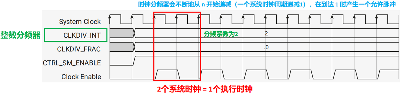
The clock divider does not reduce the system clock rate; instead, it defines how many system clock cycles correspond to "one cycle" of PIO program execution. It generates a clock enable signal that can pause or resume execution in each system clock cycle. The essence of the clock divider is to generate a "Clock Enable signal" to control the execution rhythm of the finite-state machine:
When Clock Enable is high, the finite-state machine executes one instruction;
When Clock Enable is low, the finite-state machine pauses execution (while the system can still access its FIFO and modify the configuration).
A clock divider can simplify the interface between the finite-state machine and the system, reduce latency, and occupy a very small chip area. When the clock enable signal is at a low level, the finite-state machine is completely in an idle state, but the system can still access the FIFO of the finite-state machine and change its configuration.
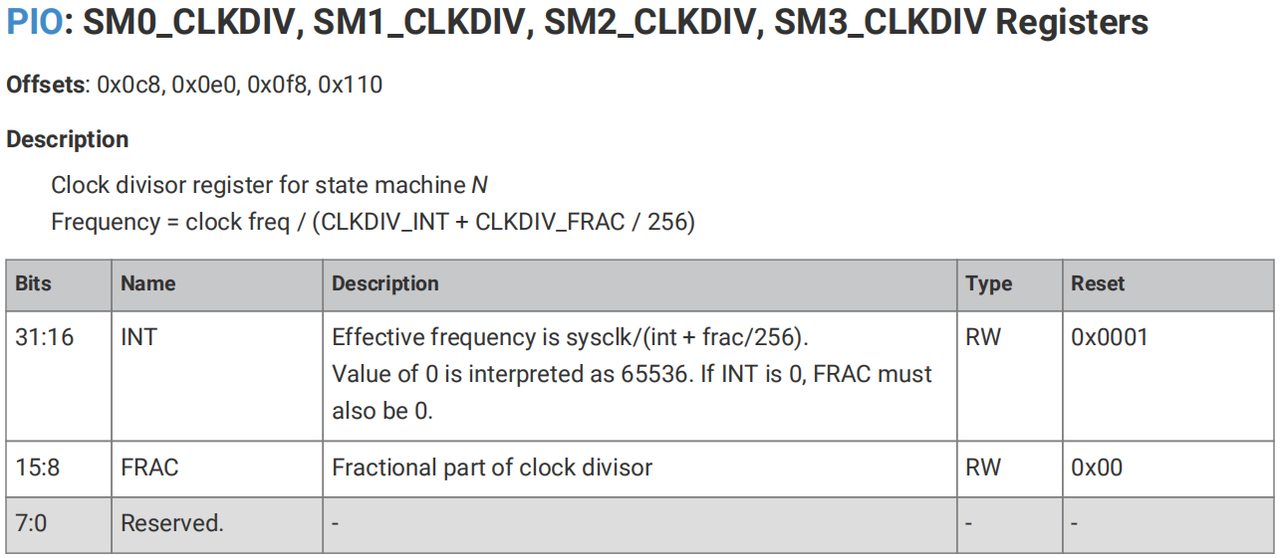
The clock divider supports frequency division with an integer part of 16 data bits and a fractional part of 8 data bits, and the fractional divider adopts a first-order delta-sigma structure. The clock division ratio can be adjusted in increments of 1/256 within the range of 1 to 65536.
If the clock division ratio is set to 1, the finite-state machine will execute in every clock cycle, namely, run at full speed:
Typically, using only an integer frequency divider causes the finite-state machine to operate at a rate where n clock cycles correspond to 1 execution cycle, resulting in an effective clock rate of f (sys) / n.
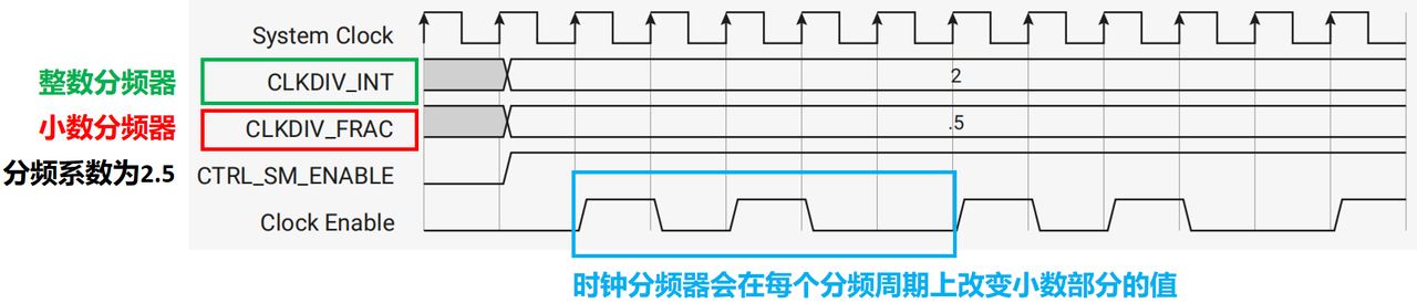
When a more accurate rate is required (such as 2.5 times frequency division), integers alone are not enough. In this case, fractional division is used. By combining "integer part + fractional part", "non-integer system clocks correspond to one execution cycle" is achieved. The value of the fractional divider is equal to n + f/256 , where n and f are the integer and fractional parts of the CLKDIV register of the fine-state machine. It selectively extends a certain frequency division period between n cycles and n + 1 cycles.
We can see that:
The actual frequency division ratio of the frequency divider = integer part (INT) + fractional part (FRAC/256)(FRAC is 8-bit, ranging from 0 to 255, corresponding to a fraction between 0 and 1);
Adopt the "first-order integral-differential (delta-sigma)" algorithm: use n system clocks in most cycles and occasionally n+ 1 system clocks, so as to achieve a fractional division ratio on average.
In the figure:
The integer part INT = 2, and the fractional part FRAC = 128 (since 0.5 = 128/256);
The frequency divider alternately generates enable pulses using 2 and 3 system clocks, which averages out to 2.5 system clocks per execution cycle;
When the integer division factor n is small, the jitter caused by the fractional division ratio may be unacceptable. However, when the integer division factor n is very large, the jitter is almost negligible.
It should be noted that for high-speed asynchronous serial ports, it is recommended to use an even frequency division ratio or an integer multiple of 1 Mbaud, rather than the traditional multiple of 300, to avoid unnecessary jitter.
6. GPIO Mapping
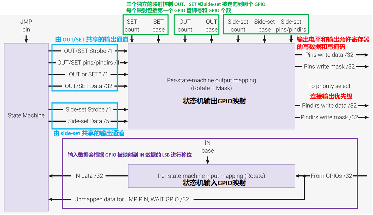
GPIO mapping refers to the hardware connection rules between the PIO finite-state machine and external GPIO pins, which are divided into two categories: "output mapping (finite-state machine → GPIO)" and "input mapping (GPIO → finite-state machine)". It determines the specific GPIO pins controlled or read by finite-state machine instructions (OUT/SET/side-set/IN), and serves as the core flexible feature for PIO to adapt to different peripheral pin layouts.
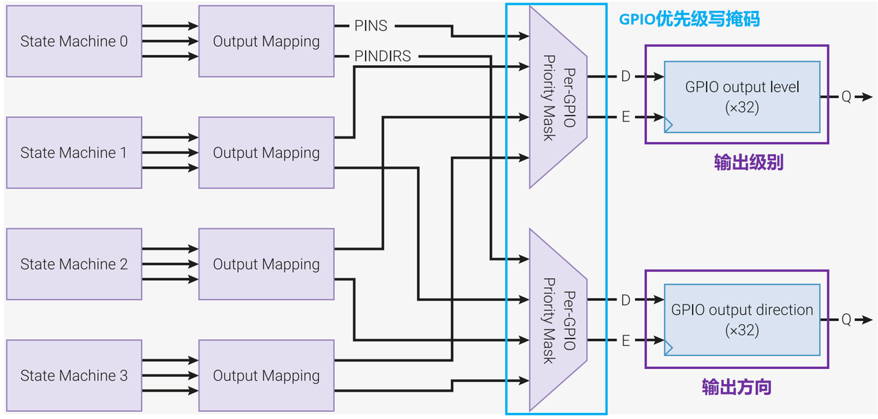
Internally, the PIO has a 32-bit register that represents the output level of each GPIO pin it can drive, and another register that indicates the enable state (high or low impedance) for each output;During each system clock cycle, each finite-state machine can write to some or all of these GPIO registers.
The write data and write mask of the output level and output enable register come from the following sources:
An OUT instruction can write up to 32 data bits. Depending on the Destination field of the instruction, the instruction can be applied to the pin or pin direction. The lowest bit of the OUT data maps to the PINCTRL_OUT_BASE , sequentially maps PINCTRL_OUT_COUNT data bits backward, and returns after reaching GPIO31.
A SET instruction can write up to 5 data bits. Depending on the Destination field of the instruction, the instruction can be applied to the pin or discipline direction. The lowest bit of the SET data maps to the PINCTRL_SET_BASE , sequentially maps PINCTRL_SET_COUNT data bits backward, and returns after reaching GPIO31.
A side-set operation can write up to 5 data bits. Depending on the value of the EXECCTRL_SIDE_PINDIR register field, this operation can be applied to pins or pin directions. The least significant bit of the side-set data is mapped to PINCTRL_SIDESET_BASE, and the subsequent PINCTRL_SIDESET_COUNT data bits are mapped sequentially backward, wrapping around after reaching GPIO31.
Each OUT / SET /side-set operation writes to a consecutive pin range, yet each range has its own independent size and location within the 32-data-bit GPIO space. This is already sufficiently flexible for most applications. For instance, if one finite-state machine implements an interface such as SPI on a set of pins, another finite-state machine can run the same program, mapped to a different set of pins, to provide a second SPI interface.
During any clock cycle, the finite-state machine can execute one OUT or SET, and can simultaneously execute one side-set. The pin mapping logic generates a write mask of 32 data bits, and writes the output level and output enable registers to the data bus according to the request content and pin mapping configuration.
If the side-set operation of the same finite-state machine within the same clock cycle overlaps with the OUT / SET operation, side-set takes precedence in the overlapping area.
6.1 Output Priority
Output Mapping Control OUT / SET / side-set the GPIO pins corresponding to the instructions, with the core rules as follows:
Independent mapping interval configuration: OUT / SET / side-set each configure their mapping range via dedicated registers:
OUT: Determined by PINCTRL_OUT_BASE (starting GPIO number) and PINCTRL_OUT_COUNT (number of pins), the least significant bit of data corresponds to OUT_BASE, and subsequent GPIOs are mapped in sequence (wrapping around after GPIO31);
SET: determined by PINCTRL_SET_BASE and PINCTRL_SET_COUNT, following the same rules as OUT;
side-set: determined by PINCTRL_SIDESET_BASE and PINCTRL_SIDESET_COUNT, following the same rules as OUT;
Operation priority in the same cycle: if a finite-state machine executes side-set and OUT/SET within the same clock cycle, and the GPIOs mapped by the two overlap, the side-set operation takes effect preferentially (overwriting the corresponding pin values of OUT/SET);
Write Data and Mask: Each output operation generates 32-bit "write data" and "write mask"; only the GPIOs covered by the mask will be modified, while the uncovered GPIOs remain in their original state.
6.2 Output Priority
Each finite-state machine selects the priority for each GPIO via a write mask. For each GPIO, the logic takes into account the write levels and directions from the four finite-state machines, and then applies the value from the finite-state machine with the highest number.
Each finite-state machine executes once per cycle via its pin mapping hardware OUT / SET and side-set. In this way, each finite-state machine generates 32-bit write data and write masks for the GPIO output level and output enable registers.
For each GPIO, the PIO considers write operations from all four finite-state machines, then applies the write operation from the finite-state machine with the highest number. This step is performed separately for the output level and output value, so it is possible that within the same cycle, one finite-state machine simultaneously changes both the level and direction of the same pin (for example via concurrently issued SET and side-set), or one finite-state machine changes the GPIO direction while another finite-state machine changes the level of the same GPIO. If no finite-state machine writes to the level or direction of a GPIO, the value remains unchanged.
6.3 Input Mapping
IN receives instruction data in such a manner that the LSB is mapped to the GPIO set by PINCTRL_IN_BASE, subsequent higher bits come from GPIOs with sequentially higher numbers, and the sequence wraps around when reaching bit 31.
In other words, the IN bus is the result of right-shifting the GPIO input value by PINCTRL_IN_BASE bits. If there are fewer than 32 GPIOs, the PIO input will be padded with 0s at the corresponding positions to make up the full 32 data bits.
Instructions such as WAIT GPIO use absolute GPIO numbers instead of the indices in the IN data bus, and no right shift operation will be performed in this case.
6.4 Input Synchronizer
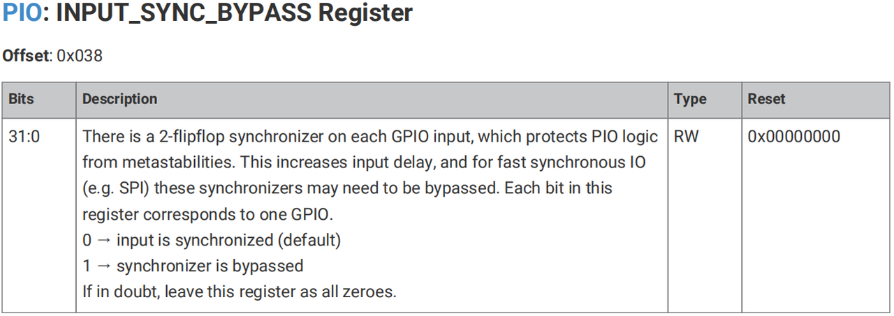
To ensure the stability of PIO, each GPIO input is equipped with two standard 2-flip-flop synchronizers, which will result in a two-cycle delay in input sampling. However, the advantage of this is that the finite-state machine can execute IN PINS at any time, and only clean high and low levels will be observed, without any intermediate values that may interfere with the finite-state machine circuitry. This is particularly critical for asynchronous interfaces such as UART RX.
Sometimes, certain GPIOs may require bypassing the synchronizer. This reduces latency, but users must ensure on their own that the finite-state machine does not sample at the wrong time. Typically, only synchronous interfaces such as SPI can achieve this. Set the corresponding data bit in INPUT_SYNC_BYPASS to bypass the synchronizer.
It should be noted that sampling unstable inputs will lead to unpredictable behavior of the finite-state machine, which should be avoided.
We can configure or read the synchronizer by accessing the INPUT_SYNC_BYPASS register:
7. Instruction Execution
In addition to the instruction memory, the finite-state machine can also execute instructions from three other sources:
MOV EXEC can execute instructions from a register specified by Source:
MOV EXEC, <source>: source (e. g., X/Y/ISR/OSR) as the instruction to execute.
The MOV instruction consumes 1 cycle, and the instruction in the register is executed in the next cycle.
OUT EXEC can execute the data migrated out via OSR:
OUT EXEC, <bit_count> Executes the 16-bit data shifted out from OSR as an instruction;
The OUT instruction consumes 1 cycle, and the instruction will be executed in the next cycle.
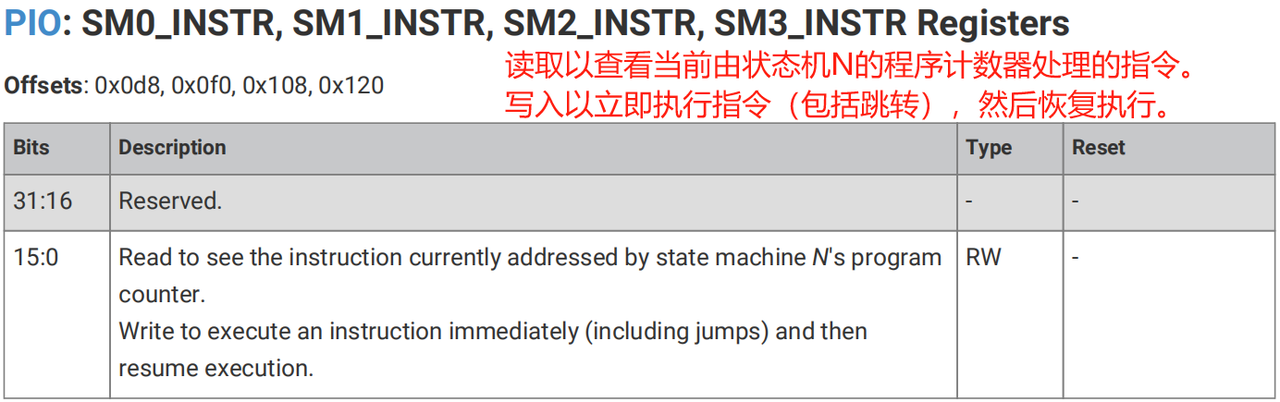
Execute instructions from the SMx_INSTR control register; the system can directly write instructions to this register for immediate execution:
Fetch: Obtain the instruction pointed to by the current program counter (PC);
Write: Write a 16-bit instruction to the register, and the finite-state machine will execute the instruction immediately.
In the following sample program, we load 32 data bits from the TX FIFO in a loop, then execute the lower 16 data bits as an instruction (since a 32-bit instruction will be written to the INSTR register, and only the lower 16 bits of the INSTR register are accessible).
The PIO program is as follows:
.program exec_example

hang:
    jmp hang ; 定义了一个标签 hang,并在这里形成一个无限循环跳转
execute:
    out exec, 32
    jmp execute ; 定义了另一个标签 execute,在这里无限循环地将寄存器中的 32 位数据输出并执行

.program instructions_to_push

    out x, 32 ; 将 32 位数据从寄存器 x 输出
    in x, 32 ; 将 32 位数据从输入端口载入到寄存器 x
    push ; 将寄存器 x 中的数据推送到 TX FIFO
The C language program that calls the PIO program is as follows, and this program will output "12345678" when running:
#include "tb.h" // TODO this is built against existing sw tree, so that we get printf etc

#include "platform.h"
#include "pio_regs.h"
#include "system.h"
#include "hardware.h"

#include "exec_example.pio.h"

int main()
{
    tb_init();

    // 将 exec_example_program 数组中的指令加载到 PIO 指令存储器中
    for (int i = 0; i < count_of(exec_example_program); ++i)
        mm_pio->instr_mem[i] = exec_example_program[i];

    // 配置状态机 0 的 SHIFTCTRL 寄存器,启用自动拉取功能,并设置拉取计数器阈值为 32
    mm_pio->sm[0].shiftctrl = (1u << PIO_SM0_SHIFTCTRL_AUTOPULL_LSB);

    // 启动状态机 0,使其进入 hang 死循环
    hw_set_bits(&mm_pio->ctrl, 1u << (PIO_CTRL_SM_ENABLE_LSB + 0));

    // 强制状态机跳转到 execute 标签的位置,开始执行 out exec, 32 指令
    mm_pio->sm[0].instr = 0x0000 | 0x1; // jmp execute

    // 写入 instructions_to_push_program 中的指令到TX FIFO
    // 写入一些数据(12345678)到TX FIFO
    mm_pio->txf[0] = instructions_to_push_program[0]; // out x, 32
    mm_pio->txf[0] = 12345678;                        // data to be OUTed
    mm_pio->txf[0] = instructions_to_push_program[1]; // in x, 32
    mm_pio->txf[0] = instructions_to_push_program[2]; // push

    // 等待 RX FIFO 中有数据可读,并将其打印出来
    while (mm_pio->fstat & (1u << PIO_FSTAT_RXEMPTY_LSB))
        ;

    printf("%d\n", mm_pio->rxf[0]);

    return 0;
}
The C program sets the finite-state machine to the running state, then enters a hang loop. While the finite-state machine is executing, the C program enforces a jmp instruction to make the finite-state machine jump out of the loop.
When an instruction is written to the INSTR register, the finite-state machine will immediately decode and execute this instruction instead of executing the instruction read from the PIO instruction memory. The program counter will not increment, so in the next cycle (assuming the instruction forced by the INSTR register does not cause a wait state), the finite-state machine will continue executing the current program from the original position, unless the written instruction modifies PC.
Write to the INSTR register: the delay cycles in the instruction will be ignored and the instruction will be executed immediately, regardless of the setting of the clock divider of the finite-state machine. This interface is used to perform initialization or process flow control change, so the instruction will be executed as soon as possible regardless of the configuration of the finite-state machine.
Writing to INSTR may trigger a wait state, during which the finite-state machine locks the instruction until it is completed. When this occurs, the EXECCTRL_EXEC_STALLED flag will be set. Resetting the finite-state machine or writing INSTR with NOP can clear this flag.
The second phase of the PIO program for the finite-state machine in the above example uses the OUT EXEC instruction. OUT itself requires one execution cycle, and the instruction executed by OUT will be carried out in the next execution cycle. Note that one of the instructions being executed is also OUT — the finite-state machine can only execute one OUT instruction per cycle.
OUT EXEC writes the data shifted out by OUT into the internal instruction register. In the next cycle, the finite-state machine knows that it should not execute the instruction memory, but instead execute the content of this latch, and also knows that it should not increment PC at this point.
Note that if an instruction written to INSTR causes a wait state, this instruction will be written to the same instruction register used by OUT EXEC and MOV EXEC, overwriting the instruction stored therein. Therefore, if the EXEC instruction is used, the instruction written to INSTR must not cause a wait state.