This article introduces RP2040's multi-rail power supply system and several practical power supply wiring schemes.
COMPONENTS
PROJECT DESCRIPTION
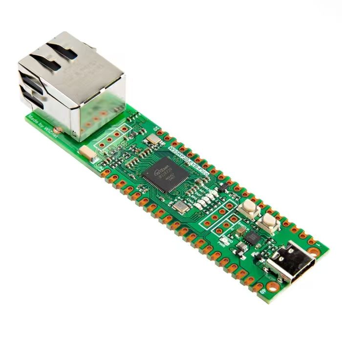
【Preliminary Note】The original hardware example in this article was written based on the RP2040. The actual hardware used in this hands-on demonstration features the W55RP20 as the main controller chip. The circuit logic and UF2 flashing operation principles are universally applicable, with only the main controller model differing. The original chip model mentioned in the circuit descriptions below is provided for reference purposes only.
Power Supply System
The power supply system serves as the "energy source" of the RP2040. For the chip to function, power must be supplied to different functional modules (such as pins, core logic, USB, and ADC). The RP2040 requires five independent power supplies, but in most applications, some of these power supplies can be combined and connected to a single power source.
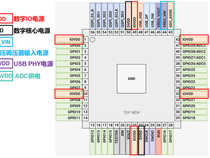
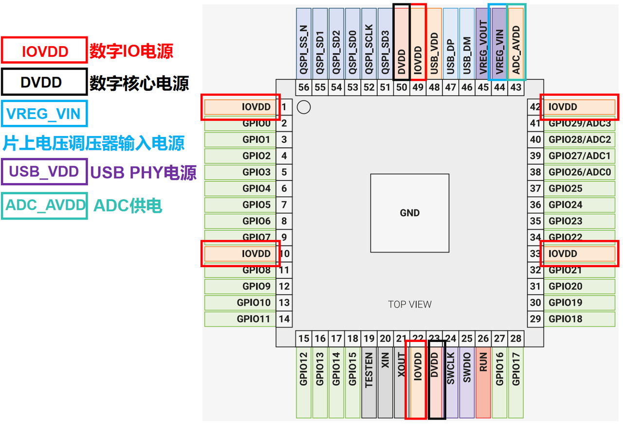
Figure 2.22 Schematic Diagram of RP2040 Power Supply System Pins and Power Supply Classification
Although the official documentation states that 5 independent power supplies are required, in practical project implementation, there is almost no need to connect all 5 of them. This is because the chip comes with a built-in "voltage regulator", which can convert a single 3.3V power supply into the voltages required by other modules. Therefore, in most scenarios, connecting just one 3.3V power supply is sufficient to ensure the chip operates properly.
1. Digital IO Power Supply (IOVDD)
IOVDD is the power supply for the "external pins (IO ports)" of the chip, which is responsible for "providing a voltage reference" for signals during communication between the pins and external devices (such as sensors and display screens). For example, if you need to connect a 3.3V sensor, IOVDD should be connected to 3.3V; if you need to connect a 1.8V device, IOVDD should be connected to 1.8V (the applicable range is 1.8V-3.3V).
IOVDD should be connected to a 100nF capacitor close to the IOVDD pin of each chip.
2. Digital Core Power Supply (DVDD)
DVDD serves as the power supply for the "internal core logic" of the chip (equivalent to the "heart power supply" of the chip), which is responsible for powering core modules such as the kernel, memory, and bus, with a rated voltage of 1.1V.
However, there is no need to connect a separate 1.1V power supply, as the chip integrates an on-chip voltage regulator (VREG_VOUT) that can convert IOVDD (or other 1.8V-3.3V power supplies) into 1.1V DVDD; simply connect the output of the regulator to the DVDD pin externally on the chip.
If required, DVDD can be powered by an off-chip power supply. A 100nF capacitor shall be placed close to each DVDD pin of the chip.
3. On-Chip Voltage Regulator Input Power Supply (VREG_VIN)
This is the "input power supply" of the chip's "internal voltage regulator". For the voltage regulator to step down a high voltage to the 1.1V of DVDD, it first needs to be powered itself, and VREG_VIN serves this purpose. It has an input voltage range of 1.8V to 3.3V, and VREG_VIN can be connected to the same power supply as IOVDD, which eliminates the need for an additional external power supply.
A 1μF capacitor shall be connected between VREG_VIN and the ground line of the VREG_VIN pin close to the chip.
4. USB PHY Power Supply (USB_VDD)
This is the power supply for the "USB function module" of the chip, which is responsible for USB communication (such as program flashing and connection to a computer). It has a rated voltage of 3.3V and can share the same 3.3V power supply with IOVDD.
USB_VDD shall be decoupled with a 100nF capacitor placed close to the USB_VDD pin of the chip.
5. ADC Power Supply (ADC_AVDD)
ADC_AVDD serves as the power supply for the on-chip "ADC (Analog-to-Digital Converter)", which is responsible for converting analog signals (such as voltage) from sensors into digital signals, and its supply voltage directly affects conversion accuracy: it can operate at a nominal supply voltage ranging from 1.8V to 3.3V, but when the voltage drops below 2.97V, the performance of the ADC will be degraded. To reduce the number of external power supplies, ADC_AVDD can share the same power supply as the digital IO power supply (IOVDD).
It is safe to supply ADC_AVDD at a voltage higher or lower than IOVDD; for example, power the ADC at 3.3V for optimal performance while supporting 1.8V signal levels on the digital IOs. However, the voltage of the ADC analog input must not exceed IOVDD. For instance, if the IOVDD voltage is 1.8V, the ADC input voltage should be limited to 1.8V. A voltage higher than IOVDD will cause leakage current through the ESD protection diode.
6. Power On/Off Sequence
The power supplies of the RP2040 can be powered on or off in any order.
However, if the ADC power supply (ADC_AVDD) is powered on before the digital core power supply (DVDD) or powered off after the latter is powered off, a small transient current may be generated in the ADC power supply (ADC_AVDD). This will not damage the chip, but can be avoided by turning on DVDD before or simultaneously with ADC_AVDD, and turning off DVDD after or simultaneously with ADC_AVDD.
In the most common power supply scheme, the chip is powered by a single 3.3V power supply. Due to the startup time of the voltage regulator on the chip, DVDD will start up shortly after ADC_AVDD.
7. Power Supply Scheme
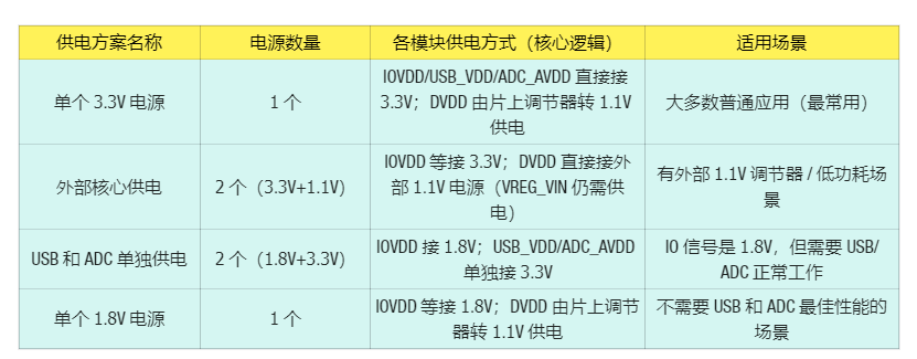
7.1 Single 3.3V Power Supply
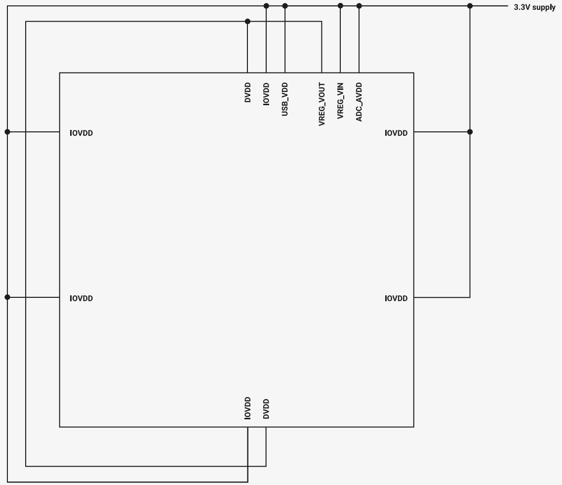
In most applications, the RP2040 will be powered by a single 3.3V power supply. The digital I/O (IOVDD), USB PHY (USB_VDD) and ADC (ADC_AVDD) will be directly powered by the 3.3V supply, while the 1.1V digital core power supply (DVDD) will be regulated from the 3.3V supply by the on-chip voltage regulator. Note that the regulator output pin (VREG_VOUT) must be connected to the off-chip DVDD pin.
Schematic diagram of the single 3.3V power supply scheme for RP2040 in Figure 2.23
7.2 External Core Power Supply
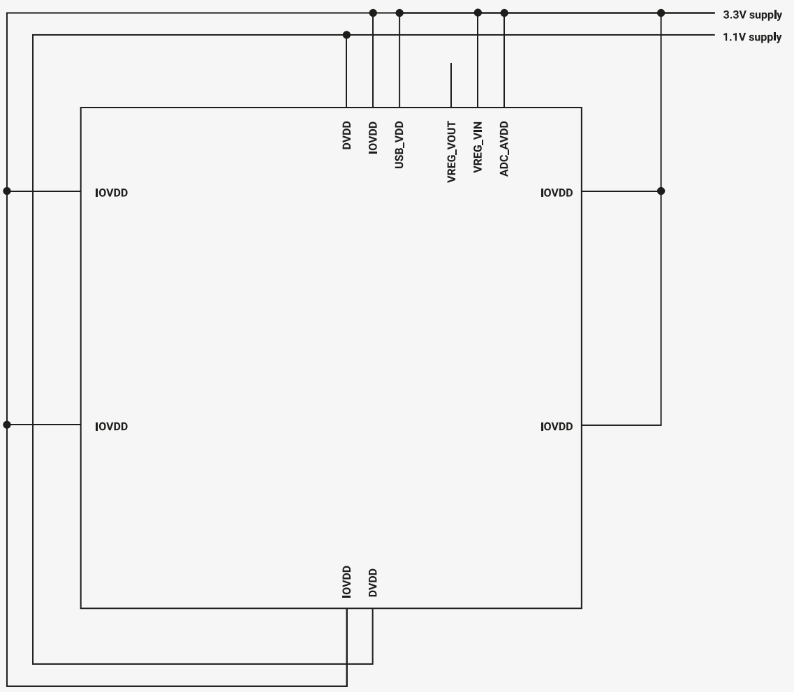
The digital core (DVDD) can be directly powered by an external 1.1V power supply instead of the on-chip regulator; this approach may be worthwhile if a suitable external regulator is available elsewhere in the system, or if it can replace the inefficient linear on-chip voltage regulator for low-power applications.
In this case, the output of the on-chip voltage regulator (VREG_VOUT) should not be connected to DVDD, while power still needs to be supplied to the regulator input (VREG_VIN) to enable the chip's power-on reset and power-loss detection functions. The on-chip voltage regulator will power up immediately once VREG_VIN is available, but it can be turned off under software control as soon as the chip exits reset.
Schematic Diagram of RP2040 External 1.1V Core Power Supply Scheme (Figure 2.24)
7.3 Independent Power Supply for USB and ADC
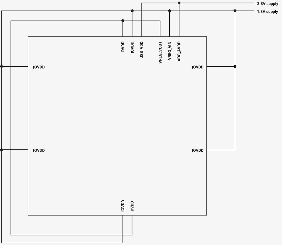
For applications where the digital IO signal level is lower than 3.3V, a separate 3.3V power supply will be required for the USB PHY and ADC, as the USB PHY fails to meet the specifications when the voltage drops below 3.135V, and the performance of the ADC is compromised when the voltage is lower than 2.97V.
In the figure below, the digital IO (IOVDD) is powered by 1.8V, and provides separate 3.3V power supplies for the USB PHY (USB_VDD) and the ADC (ADC_AVDD). The regulator input terminal (VREG_VIN) is connected to the 1.8V power supply, although it can equally be connected to the 3.3V power supply. If the 1.8V power supply is generated by an efficient switching mode regulator, connecting it to the 1.8V power supply will reduce the overall power consumption.
Figure 2.25 RP2040 USB and ADC separate 3.3V power supply scheme schematic diagram
7.4 Single 1.8V Power Supply
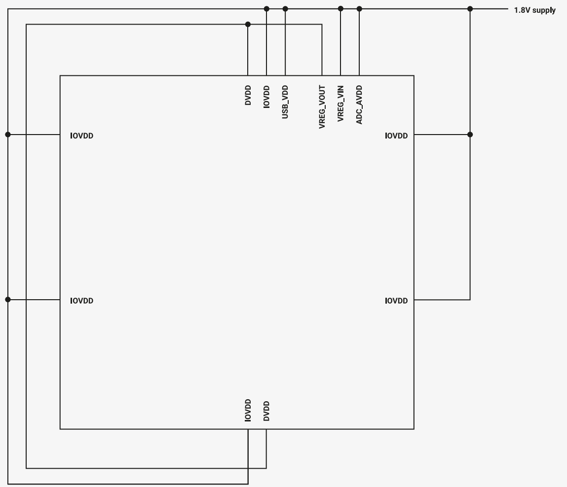
If the functional USB PHY and optimal ADC performance are not required, the RP2040 can be powered by a single power supply of less than 3.3V. The DVDD is regulated from the 1.8V power supply by the on-chip voltage regulator.
Schematic Diagram of RP2040 Single 1.8V Power Supply Scheme (Figure 2.26)