Must-Know for Embedded Beginners: All MCUs Do Not Run the main Function First Upon Power-On
This article introduces RP2040’s power-on boot sequence, covering hardware initialization and BootROM-driven Flash/USB boot modes.
COMPONENTS
PROJECT DESCRIPTION
BOOT Boot Sequence
The "boot sequence" of a chip is just like the entire process that takes place after we power on a computer, from the "black screen, power-off state" to the point where the system boots up and can run software — after the RP2040 is powered on (supplied with power) or reset, it will not directly run the program we wrote, but will first execute the built-in "boot process" of the chip, which is divided into two steps: preparation work at the hardware level and execution of the bootloader at the software level.Bootrom (boot ROM) is the core boot code embedded in the 16kB ROM of the chip. As we mentioned earlier, ROM is the storage that is pre-programmed into the chip during manufacturing, and bootrom serves as the "boot kit" within it, acting as the core executor of the entire boot process.
The startup process here can be divided into the following two steps:
Hardware controlled: Refers to the operations performed by the chip before the bootrom bootloader is executed. The bootrom bootloader is software built into the chip, and this process does not require software involvement, belonging to the self-initialization of the chip hardware;
Processor controlled: Executes the bootrom bootloader, which falls under the execution of a software boot program.
1. hardware-controlled boot sequence
When the chip is powered on, the RUN pin is set: the RUN pin acts as the "power-on switch" of the chip, and "setting" refers to toggling this switch to the "ON" state to inform the chip that "power has been connected and startup can begin";
The on-chip voltage regulator waits for the digital chip power supply (DVDD) to stabilize:
A voltage regulator is a "voltage stabilizer" that supplies power to the "digital circuit" inside the chip (similar to the voltage stabilization function of a mobile phone charger); DVDD is the dedicated power supply for digital circuits;
This step is to wait for the voltage of DVDD to stabilize at a safe value (e. g., 1.8V), so as to prevent the internal circuit of the chip from being burned out by fluctuating voltage, which is equivalent to the fact that the power supply of a computer will wait until the output voltage stabilizes before supplying power to the motherboard during startup.
The power-on finite-state machine has been started. As an automatic circuit in the chip responsible for completing hardware preparation in sequence, it will carry out the following tasks in order:
The ROSC (Ring Oscillator) has started and provides a clock source for the clock generator, with clk_sys and clk_ref now operating at a relatively low frequency (typically 6.5 MHz):
ROSC serves as the "initial clock source" of the chip (equivalent to the "mainspring" of an alarm clock), and upon startup, it generates the fundamental "clock signal" — the "heartbeat rhythm" that governs the chip's operation;
clk_sys serves as the "main system clock" of the chip, while clk_ref acts as the "reference clock". The initial operation at a low frequency (6.5MHz) is designed to ensure safer and more stable hardware startup, and the frequency will be increased subsequently as required.
The reset controller, XIP execute-in-place hardware, memory, bus architecture, and processor subsystem all exit the reset state:
These hardware modules are in a "reset state"(equivalent to "sleep lock") when power is cut off;
"Exit Reset" refers to waking up and unlocking these modules to bring them into a "operable state", for example, the memory is ready to store data, the bus is ready to transmit data, and the processor core is ready to execute programs.
Processor core 0 and core 1 start executing the boot program: after all hardware is ready, the two processor cores are woken up and start executing the bootrom boot program built into the chip, and the hardware-controlled boot process ends here.
2. Processor-controlled boot sequence
The processor-controlled boot sequence is the "task allocation + boot mode selection process" initiated after the bootrom bootloader starts executing. At this point, the hardware is already ready; the bootrom (the "boot manager" embedded in the chip) first assigns tasks to the two cores, then determines "where to load the user program" — either reading the program from external Flash or entering USB mode to wait for user program flashing — and the entire process is completed automatically by "evaluating various hardware signals and executing preset logic".
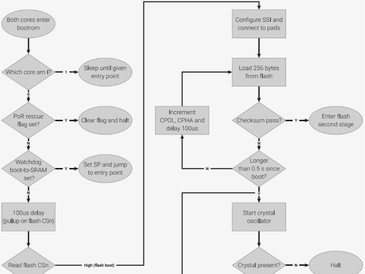
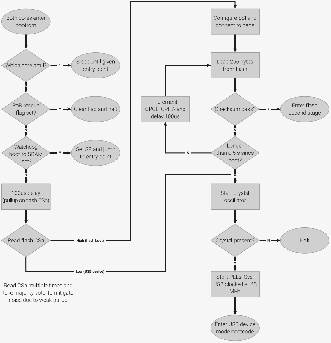
Figure 2.21 Flowchart of the boot sequence controlled by the RP2040 processor
The first part is the initial division of labor for the dual-core (on the left side of the flowchart). After both cores (Core0 and Core1) enter the bootrom, they first complete the "responsibility division":
"Which core am I? ": Both cores run simultaneously, but their identities are distinguished via the previously mentioned "CPUID register":
If it is Core1: enter the "Sleep until given entry point" state (i. e., sleep and wait for Core0 to assign tasks to it);
If it is Core0: proceed with the subsequent boot logic (Core0 is the "primary boot core").
"PoR rescue flag set? ": This is the "fault rescue switch" of the chip: if this flag is enabled, it indicates that a previous startup failure has occurred, and Core0 will perform "Clear flag and halt" to wait for manual troubleshooting.
"Watchdog boot-to-SRAM set? "(Does the watchdog require booting from SRAM?): The watchdog acts as the chip's "fault reset utility": if the watchdog is configured to boot from SRAM, Core0 will execute "Set SP and jump to entry point"(set the stack pointer SP and jump to the program entry in SRAM) — this is the "emergency boot mode", which is typically used for debugging purposes.
"100us delay (pullup on flash CSn)":"CSn" refers to the chip select pin of the external Flash (functioning as the "switch" for the Flash). The pull-up resistor sets this pin to a high level initially (keeping the Flash unselected by default), which allocates sufficient startup time for the Flash.
"Read flash CSn"(read the CSn pin level of the Flash): Determine "whether there is an external Flash" based on the level of the CSn pin:
If it is High: it indicates that the Flash exists, and the "Flash boot" process will be executed (jump to the right side of the flowchart);
If it is Low (low level): it indicates that there is no Flash, and the "USB boot" process will be executed (the subsequent step will enter USB mode, waiting for the user to program via USB).
The second part is the boot mode selection (on the right side of the flowchart): after Core0 confirms that "Flash is present", it starts attempting to boot from Flash; otherwise, it enters USB mode.
Branch 1: Attempt Flash Boot
"Configure SSI and connect to pads"(Configure the SSI module and connect to the pins): SSI is the module that controls the QSPI interface (as mentioned earlier), and this step is to establish a communication connection between the chip and the external Flash.
"Load 256 bytes from flash": First read the "boot header data" in the Flash to verify whether the program in the Flash is valid.
"Checksum pass? ":"Checksum" serves as the "ID card" of a Flash program (equivalent to generating a "digital fingerprint" for the program):
If passed (Y): it indicates that the program in Flash is normal, and the process will enter "Enter flash second stage"(execute the secondary boot program in Flash to finally load the user program);
If No (N): continue to judge whether the startup time exceeds 0.5 seconds.
"Has it been longer than 0.5 seconds since boot? ":
If the threshold is not exceeded: adjust the communication parameters of the Flash (CPOL/CPHA are the "clock polarity/phase" of SPI, which is equivalent to "adjusting the Communication Protocol of the Flash"), then delay for 100 microseconds, and retry reading the Flash;
If it exceeds the threshold: it indicates that Flash startup has failed, and the system will switch to the "USB boot" process.
Branch 2: USB boot (after Flash boot failure)
"Start crystal oscillator": A crystal oscillator serves as a more accurate clock source, and USB communication requires a stable clock, so the crystal oscillator needs to be started first.
"Crystal present? "(Is the crystal oscillator present?):
If the crystal oscillator is absent: Core0 will "Halt" and fail to start.
If a crystal oscillator is present: proceed to the next step.
"Start PLLs. Sys, USB clocked at 48 MHz"(Start the phase-locked loops (PLLs) and set the system clock and USB clock to 48 MHz): A PLL acts as a "clock accelerator" that steps up the low-frequency clock from the crystal oscillator to the 48 MHz required by USB, which is the standard clock for USB communication.
"Enter USB device mode bootcode": At this point, the chip will act as a "USB device"(such as a USB flash drive recognized by a computer), and users can burn programs into Flash or SRAM via USB.