



MicroPython DDS: AD9833 + MCP41010 Amplitude‑Tunable Signal Generator
AD9833‑MCP41010 amplitude‑adjustable DDS implementation in MicroPython
- Custom AD9833 Class
The code below implements a custom AD9833 class for controlling the AD9833 waveform‑generator chip. It sends configuration commands over the SPI protocol to generate desired waveforms.
Sample code:
# Python env   : MicroPython v1.23.0
# -*- coding: utf-8 -*-
# @Time    : 2024/9/3 2:20 PM
# @Author  : Li Qingshui
# @File    : ad9833.py
# @Description : DDS signal chip AD9833 driver module
# Reference code: https://github.com/owainm713/AD9833-MicroPython-Module/blob/main/AD9833example.py#L54
# This code is developed by owainm713, released under GNU General Public License v3.0 License.
# ======================================== Import related modules =========================================
# Import hardware‑related modules
import machine
# Import digital‑signal‑processing‑related modules
from math import pi, radians
# ======================================== Global variables ============================================
# ======================================== Function definitions ============================================
# ======================================== Custom classes ============================================
# Custom DDS signal chip AD9833 class
class AD9833:
    """
    AD9833 class for controlling the AD9833 waveform‑generator chip. Communicates with host MCU over SPI interface and configures output waveform, frequency and phase.
    This class provides full control functions for AD9833, including setting waveform type (sine, square, triangle), adjusting frequency and phase, and supporting dynamic parameter modification during runtime.
    Attributes:
        fmclk (int): Master clock frequency in Hz, default 25 MHz.
        sdo (machine.Pin): SPI data‑output pin for data transmission.
        clk (machine.Pin): SPI clock pin for communication timing.
        cs (machine.Pin): SPI chip‑select pin for device selection.
        spi (machine.SPI): SPI communication instance for data transfer with AD9833.
        mode (str): Current operating mode, default "RESET".
        writeMode (str): Frequency‑register write mode, default write MSB and LSB simultaneously.
        freq0 (int): Stored value for frequency register 0.
        freq1 (int): Stored value for frequency register 1.
        phase0 (int): Stored phase value for phase register 0.
        phase1 (int): Stored phase value for phase register 1.
    Methods:
        __init__(self, sdo: int, clk: int, cs: int, fmclk: int = 25, spi_id: int = 0):
            Initialize AD9833 instance and configure SPI object and master‑clock frequency.
        set_control_reg(**kwargs) -> None:
            Set AD9833 control register bits to configure chip states such as reset and waveform type.
        write_data(data: int) -> None:
            Write specified data value to AD9833 registers.
        set_frequency(reg: int, freq: int) -> None:
            Configure frequency register value to set output‑signal frequency.
        set_phase(reg: int, phase: int) -> None:
            Configure phase register value to adjust output‑signal phase.
        reset() -> None:
            Reset AD9833 and re‑initialize all registers and settings.
    """
    def __init__(self, sdo: int, clk: int, cs: int, fmclk: int = 25, spi_id: int = 0) -> None:
        """
        Initialize AD9833 instance.
        Sets basic parameters including SPI pins and master‑clock frequency.
        Args:
            sdo (int): Pin number for SDATA.
            clk (int): Pin number for CLK.
            cs (int): Pin number for CS chip‑select.
            fmclk (int, optional): Master‑clock frequency in MHz, default 25 MHz.
            spi_id (int, optional): SPI peripheral index, default 0 for first SPI peripheral.
        Returns:
            None: This method returns nothing.
        Raises:
            ValueError: Raised if sdo, clk, cs are not valid pin numbers or spi_id is invalid.
        """
        if not isinstance(sdo, int) or not isinstance(clk, int) or not isinstance(cs, int):
            raise ValueError("sdo、clk、cs must be int")
        if spi_id not in (0, 1):
            raise ValueError("spi_id must be 0 or 1")
        self.fmclk = fmclk * 10 ** 6
        self.sdo = machine.Pin(sdo)
        self.clk = machine.Pin(clk)
        self.cs = machine.Pin(cs, machine.Pin.OUT)
        self.cs.value(1)
        self.spi = machine.SPI(spi_id, baudrate=1000000, polarity=0, phase=1, sck=self.clk, mosi=self.sdo)
        self.set_control_reg(B28=1, RESET=1)
        self.mode = "RESET"
        self.writeMode = "BOTH"
        self.freq0 = 0
        self.freq1 = 0
        self.phase0 = 0
        self.phase1 = 0

    def write_data(self, data: int) -> None:
        """
        Write data into AD9833 register.
        The chip uses SPI Mode 1 (CPOL = 0, CPHA = 1). Unlike standard SPI CS, FSYNC is pulled low briefly before each frame. SCLK only runs while FSYNC stays low. This protocol resembles I²S, TDM or special SPI variants used on some DSP chips.
        In short: before every write operation, manually set SCLK high, then pull chip‑select low to start communication.
        Args:
            data (int): Integer data to write into AD9833 register.
        Returns:
            None: This method returns nothing.
        Raises:
            ValueError: Raised if data argument is not integer.
        """
        data = bytearray(data)
        self.clk.value(1)
        self.cs.value(0)
        self.spi.init(baudrate=1000000)
        self.spi.write(data)
        self.cs.value(1)
        return

    def set_control_reg(self, B28: int = 1, HLB: int = 0, FS: int = 0, PS: int = 0,
                        RESET: int = 0, SLP1: int = 0, SLP12: int = 0, OP: int = 0, DIV2: int = 0, MODE: int = 0) -> None:
        """
        Assign each bit inside control register to configure AD9833 operating states including reset, output modes, frequency‑register and phase‑register selection.
        Args:
            B28 (int, optional): B28 bit for frequency‑register write mode, default 1.
            HLB (int, optional): HLB bit for high/low byte selection, default 0.
            FS (int, optional): FS bit for frequency‑register selection, default 0.
            PS (int, optional): PS bit for phase‑register selection, default 0.
            RESET (int, optional): RESET bit for reset‑state control, default 0.
            SLP1 (int, optional): SLP1 bit for sleep‑mode control, default 0.
            SLP12 (int, optional): SLP12 bit for sleep‑mode control, default 0.
            OP (int, optional): OP bit for output‑mode selection, default 0.
            DIV2 (int, optional): DIV2 bit for frequency‑divide‑by‑two function, default 0.
            MODE (int, optional): MODE bit for waveform‑output selection, default 0.
        Returns:
            None: This method returns nothing.
        Raises:
            ValueError: Raised if any parameter is not integer 0 or 1.
        """
        if B28 != 0 and B28 != 1:
            raise ValueError("B28 must be 0 or 1")
        if HLB != 0 and HLB != 1:
            raise ValueError("HLB must be 0 or 1")
        if FS != 0 and FS != 1:
            raise ValueError("FS must be 0 or 1")
        if PS != 0 and PS != 1:
            raise ValueError("PS must be 0 or 1")
        if RESET != 0 and RESET != 1:
            raise ValueError("RESET must be 0 or 1")
        if SLP1 != 0 and SLP1 != 1:
            raise ValueError("SLP1 must be 0 or 1")
        if SLP12 != 0 and SLP12 != 1:
            raise ValueError("SLP12 must be 0 or 1")
        if OP != 0 and OP != 1:
            raise ValueError("OP must be 0 or 1")
        if DIV2 != 0 and DIV2 != 1:
            raise ValueError("DIV2 must be 0 or 1")
        if MODE != 0 and MODE != 1:
            raise ValueError("MODE must be 0 or 1")
        self.B28 = B28
        self.HLB = HLB
        self.FS = FS
        self.PS = PS
        self.RESET = RESET
        self.SLP1 = SLP1
        self.SLP12 = SLP12
        self.OP = OP
        self.DIV2 = DIV2
        self.MODE = MODE
        controlReg = (B28 << 13) + (HLB << 12) + (FS << 11) + (PS << 10) + (RESET << 8) + (SLP1 << 7) + (SLP12 << 6) + (
                    OP << 5) + (DIV2 << 3) + (MODE << 1)
        controlRegList = [(controlReg & 0xFF00) >> 8, controlReg & 0x00FF]
        self.write_data(controlRegList)
        return

    def set_frequency(self, fout: int, freqSelect: int) -> None:
        """
        Calculate and write frequency‑register value to set AD9833 output‑signal frequency. Supports selecting register 0 or register 1.
        Args:
            fout (int): Target output frequency in Hz, valid range 0‑12.5 MHz.
            freqSelect (int): Select target frequency register, 0 for register 0, 1 for register 1.
        Returns:
            None: This method returns nothing.
        Raises:
            ValueError: Raised if freqSelect is not 0/1 or fout exceeds valid frequency range.
        """
        if freqSelect != 0 and freqSelect != 1:
            raise ValueError("freqSelect must be 0 or 1")
        if fout < 0 or fout > 12500000:
            raise ValueError("fout must be 0 to 12.5MHz")
        freqR = int((fout * pow(2, 28)) / self.fmclk)
        fMSB = (freqR & 0xFFFC000) >> 14
        fLSB = freqR & 0x3FFF
        if freqSelect == 0:
            addr = 0b01
            self.freq0 = fout
        else:
            addr = 0b10
            self.freq1 = fout
        fMSB = fMSB + (addr << 14)
        fLSB = fLSB + (addr << 14)
        fLSBList = [(fLSB & 0xFF00) >> 8, fLSB & 0x00FF]
        fMSBList = [(fMSB & 0xFF00) >> 8, fMSB & 0x00FF]
        fBoth = fLSBList + fMSBList
        if self.writeMode == 'MSB':
            self.write_data(fMSBList)
        elif self.writeMode == 'LSB':
            self.write_data(fLSBList)
        else:
            self.write_data(fBoth)
        return

    def set_phase(self, pout: int, phaseSelect: int, rads: bool = True) -> None:
        """
        Calculate and program phase‑register value. Supports register 0 / register 1 selection, accepts angle in radians or degrees.
        Args:
            pout (int): Target phase value (degrees if rads=False, radians if rads=True).
            phaseSelect (int): Select target phase register, 0 for register 0, 1 for register 1.
            rads (bool): True = input interpreted as radians; False = input interpreted as degrees. Default True.
        Returns:
            None: This method returns nothing.
        Raises:
            ValueError: Raised if phaseSelect is not 0 or 1.
        """
        if phaseSelect != 0 and phaseSelect != 1:
            raise ValueError("phaseSelect must be 0 or 1")
        if rads == False:
            pout = radians(pout)
        phaseR = int(pout * 4096 / (2 * pi))
        phaseR = phaseR + (0b11 << 14) + (phaseSelect << 13)
        phaseRList = [(phaseR & 0xFF00) >> 8, phaseR & 0x00FF]
        self.write_data(phaseRList)
        return

    def set_mode(self, mode: str = 'SIN') -> None:
        """
        Configure AD9833 output‑waveform type. Supported options: SIN, TRIANGLE, SQUARE, SQUARE/2, RESET, OFF.
        Args:
            mode (str): Waveform‑mode selection, default 'SIN'.
        Returns:
            None: This method returns nothing.
        Raises:
            ValueError: Raised when mode string is not inside supported list.
        """
        if mode != 'SIN' and mode != 'TRIANGLE' and mode != 'SQUARE' and mode != 'SQUARE/2' and mode != 'RESET' and mode != 'OFF':
            raise ValueError("mode must be 'SIN', 'TRIANGLE', 'SQUARE', 'SQUARE/2', 'RESET' or 'OFF'")
        self.mode = mode
        if mode == 'SIN':
            self.set_control_reg(B28=self.B28, HLB=self.HLB, FS=self.FS, PS=self.PS, RESET=0, MODE=0)
        elif mode == 'TRIANGLE':
            self.set_control_reg(B28=self.B28, HLB=self.HLB, FS=self.FS, PS=self.PS, RESET=0, MODE=1)
        elif mode == 'SQUARE':
            self.set_control_reg(B28=self.B28, HLB=self.HLB, FS=self.FS, PS=self.PS, RESET=0, SLP12=1,
                                 OP=1, DIV2=1, MODE=0)
        elif mode == 'SQUARE/2':
            self.set_control_reg(B28=self.B28, HLB=self.HLB, FS=self.FS, PS=self.PS, RESET=0, SLP12=1,
                                 OP=1, DIV2=0, MODE=0)
        elif mode == 'RESET':
            self.set_control_reg(B28=self.B28, HLB=self.HLB, FS=self.FS, PS=self.PS, RESET=1)
        elif mode == 'OFF':
            self.set_control_reg(B28=self.B28, HLB=self.HLB, FS=self.FS, PS=self.PS, RESET=1, SLP1=1, SLP12=1)
        return

    def set_write_mode(self, writeMode: str = 'BOTH') -> None:
        """
        Set frequency‑register write‑mode. Three choices: BOTH (write MSB+LSB), MSB‑only, LSB‑only.
        Args:
            writeMode (str): Write‑mode selection, default 'BOTH'.
        Returns:
            None: This method returns nothing.
        Raises:
            ValueError: Raised for invalid write‑mode string.
        """
        if writeMode != 'BOTH' and writeMode != 'MSB' and writeMode != 'LSB':
            raise ValueError("writeMode must be 'BOTH', 'MSB' or 'LSB'")
        B28 = 1
        HLB = 0
        self.writeMode = 'BOTH'
        if writeMode == 'MSB':
            B28 = 0
            HLB = 1
            self.writeMode = 'MSB'
        elif writeMode == 'LSB':
            B28 = 0
            HLB = 0
            self.writeMode = 'LSB'
        self.set_control_reg(B28=B28, HLB=HLB, FS=self.FS, PS=self.PS, RESET=self.RESET, SLP1=self.SLP1,
                             SLP12=self.SLP12, OP=self.OP, DIV2=self.DIV2, MODE=self.MODE)
        return

    def select_freq_phase(self, FS: int, PS: int) -> None:
        """
        Select active frequency register and active phase register for subsequent waveform generation.
        Args:
            FS (int): Frequency‑register select bit, 0 or 1.
            PS (int): Phase‑register select bit, 0 or 1.
        Returns:
            None: This method returns nothing.
        Raises:
            ValueError: Raised if FS or PS is not 0 or 1.
        """
        if FS != 0 and FS != 1:
            raise ValueError("FS must be 0 or 1")
        if PS != 0 and PS != 1:
            raise ValueError("PS must be 0 or 1")
        self.set_control_reg(B28=self.B28, HLB=self.HLB, FS=FS, PS=PS, RESET=self.RESET, SLP1=self.SLP1,
                             SLP12=self.SLP12, OP=self.OP, DIV2=self.DIV2, MODE=self.MODE)
        return
# ======================================== Initialization ==========================================
# ======================================== Main program ===========================================
Methods provided by our custom AD9833 class:
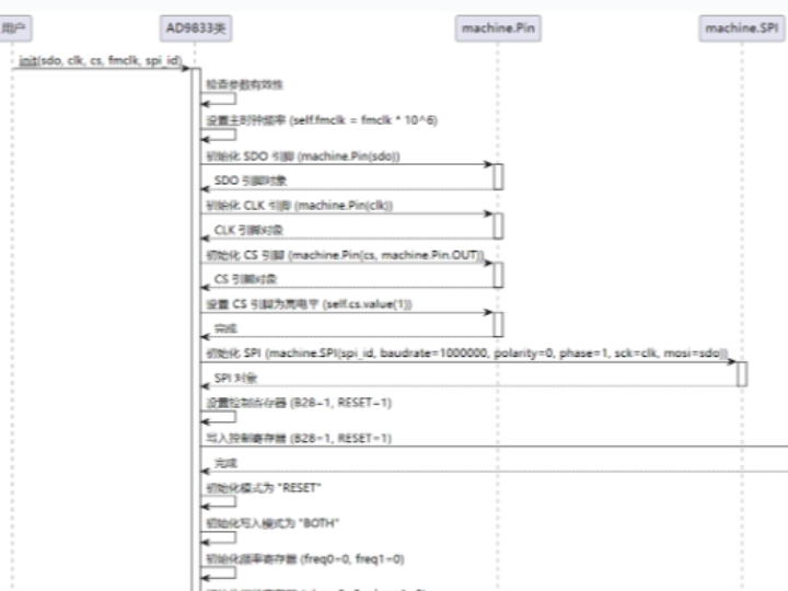
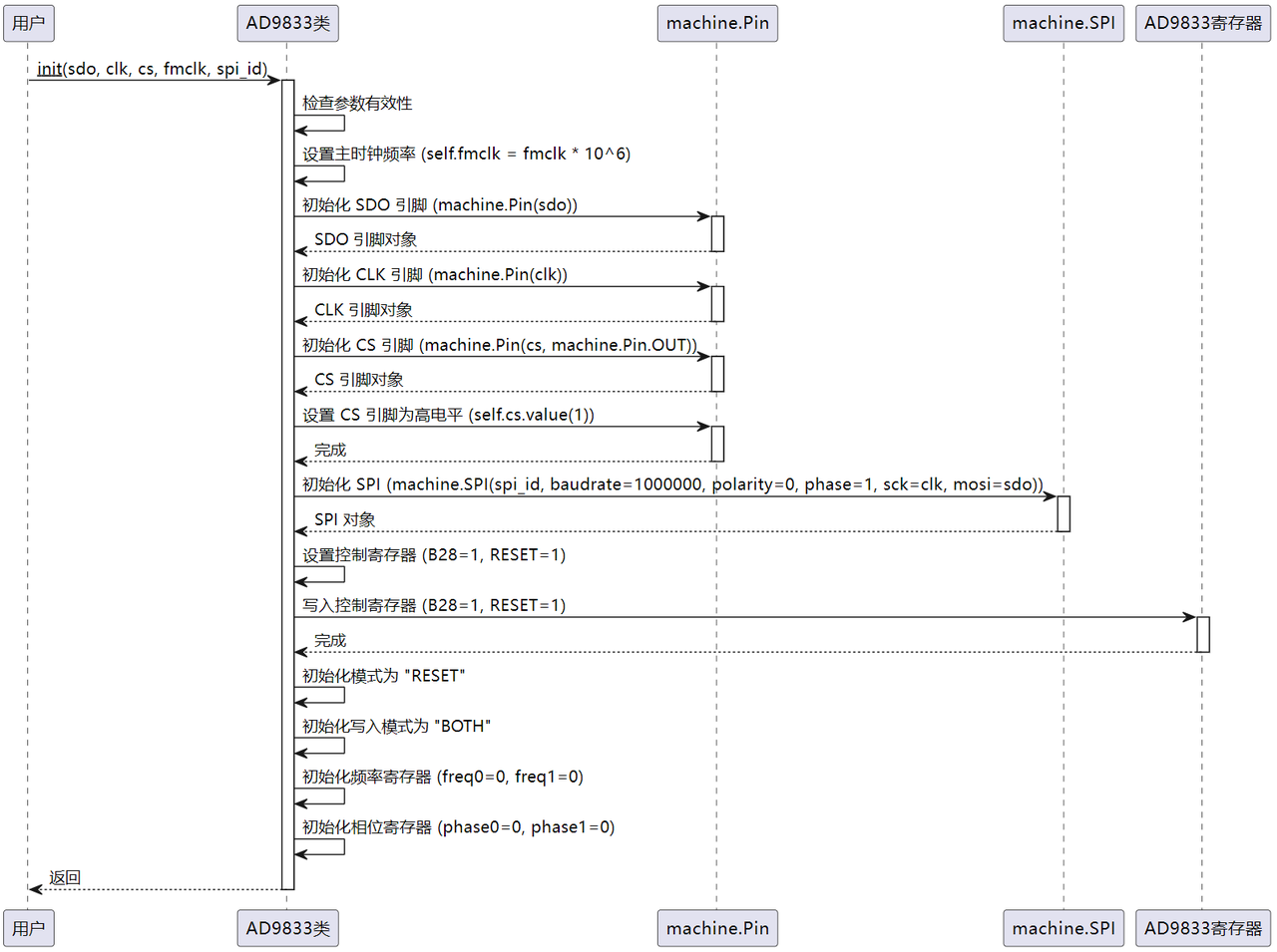
__init__ initialization method Supply pin numbers, SPI peripheral ID and master‑clock frequency (MHz). Initialize pins and peripherals, call set_control_reg() to place AD9833 into reset state, enable 28‑bit frequency‑register write mode and initialize frequency / phase registers to zero.
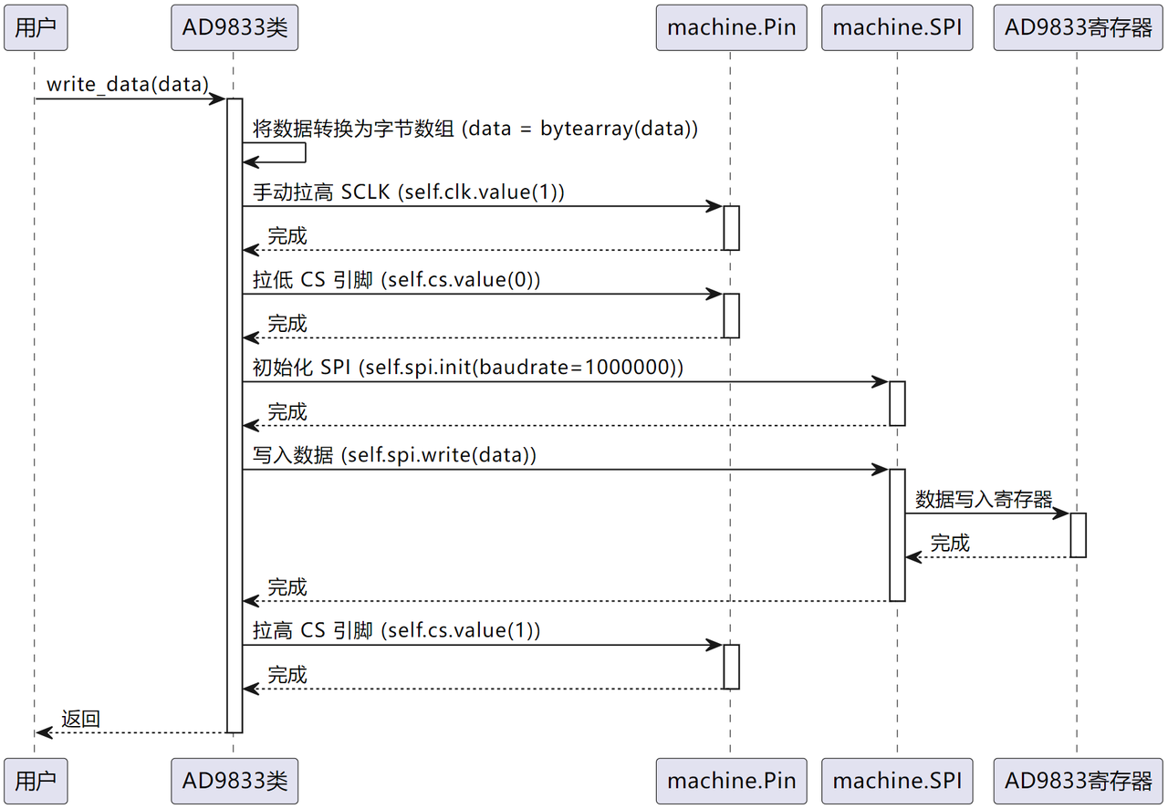
write_data SPI data‑write method Convert outgoing data into bytearray format. Manually drive SCLK high, pull CS low to start SPI communication, transmit data bytes, then pull CS high to terminate transaction.
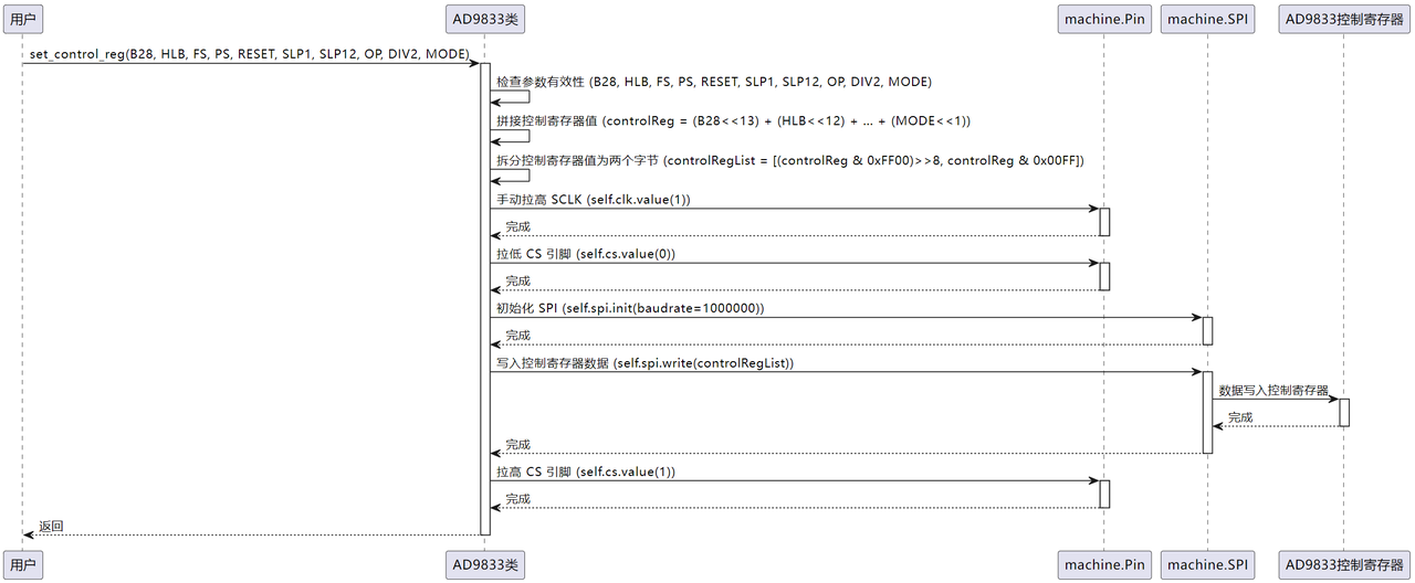
set_control_reg control‑register configuration method Build full 16‑bit control‑register value from individual bit arguments, split into two 8‑bit bytes and send via write_data. Splitting is required because MicroPython SPI defaults to 8‑bit frame length.
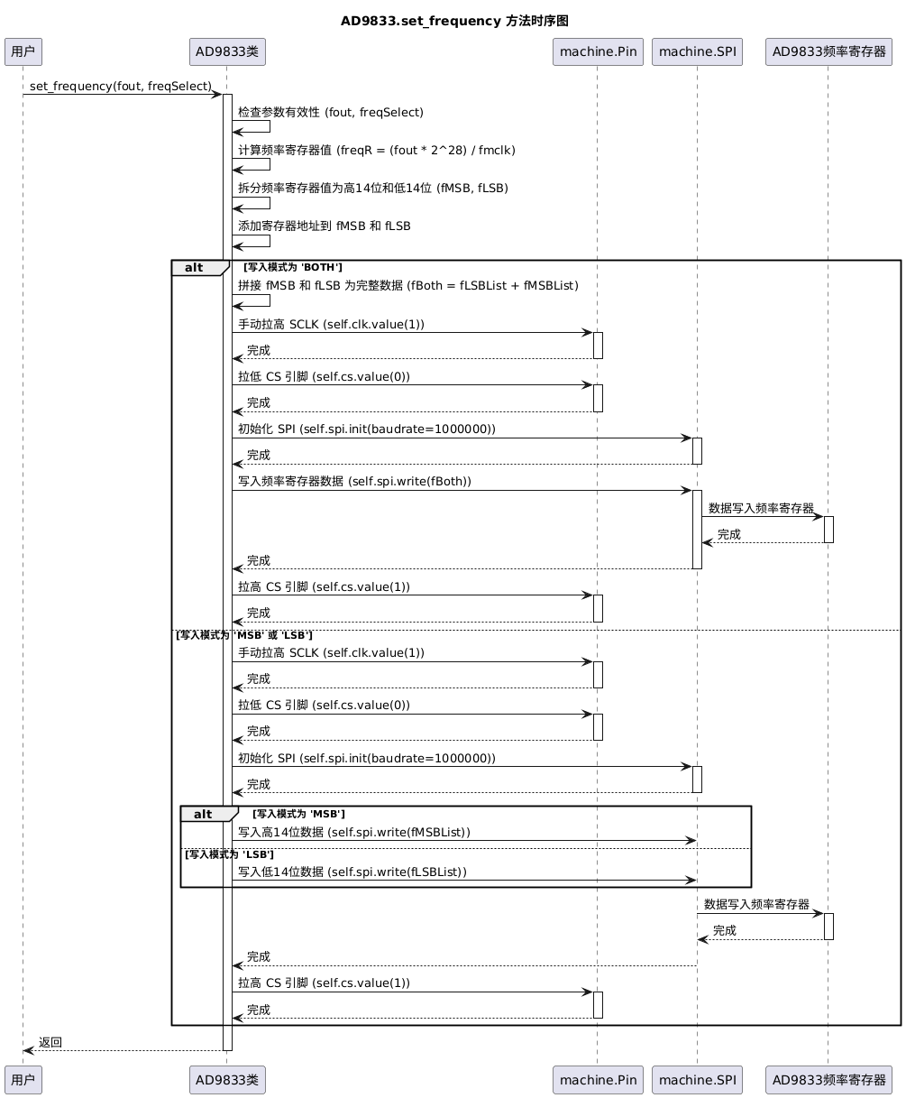
set_frequency frequency‑setting method Compute target frequency‑register value, split result into high‑14‑bit and low‑14‑bit segments, further divide each segment into two 8‑bit bytes and transmit using write_data. Supports selecting register 0 or register 1.
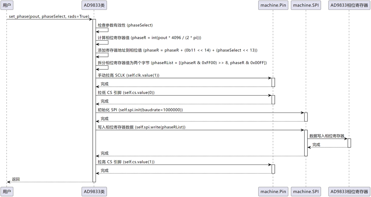
set_phase phase‑setting method Calculate phase‑register value from given phase argument, split value into two 8‑bit bytes and send via write_data.
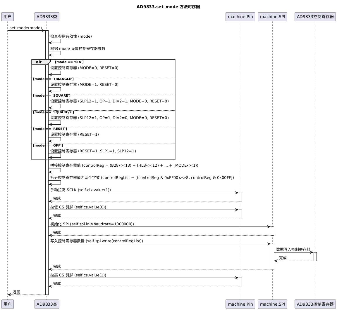
set_mode waveform‑type‑selection method Set individual control‑register bits according to selected waveform and invoke set_control_reg. Available modes: SIN, TRIANGLE, SQUARE, SQUARE/2, RESET, OFF.
set_write_mode frequency‑register write‑mode method Configure frequency‑register write behaviour: BOTH writes MSB+LSB together; MSB writes only high‑14‑bit; LSB writes only low‑14‑bit.
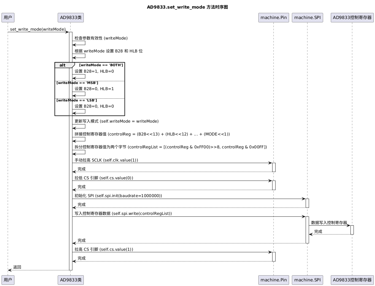
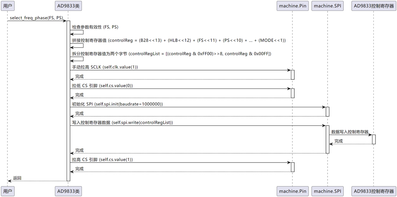
select_freq_phase frequency‑register‑and‑phase‑register‑selection method Pick which frequency register and phase register will be active. Valid inputs are 0 or 1 for each. Update control register and send settings by calling write_data.
Call‑relationship diagram for AD9833 class methods:
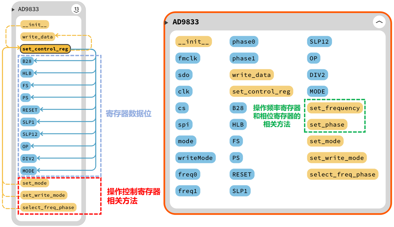
Looking at source code, methods fall into two broad groups:
Control‑register‑related methods: set_control_reg, set_mode, set_write_mode. Workflow: assign bit values, pass them to set_control_reg, which assembles and splits the value then transmits bytes to AD9833 via write_data.
Frequency‑and‑phase‑register‑related methods: set_frequency, set_phase. Workflow: convert input frequency / phase parameters into chip‑register values and send bytes through write_data.
Usage workflow for AD9833 class:
- Use
set_frequencyandset_phaseto configure output‑signal frequency and phase. - Call
select_freq_phaseto choose which pre‑programmed frequency and phase registers become active. - Invoke
set_modeto pick output‑waveform type; VOUT pin will start generating waveforms. - When stopping output, use
set_mode('OFF')to disable VOUT waveform generation. - Custom MCP41010 Class
Below is code implementing driver for MCP41010 digital potentiometer. SPI interface sends command‑and‑data bytes to set wiper value or enter shutdown mode.
# Python env   : MicroPython v1.23.0
# -*- coding: utf-8 -*-
# @Time    : 2024/12/27 11:09 AM
# @Author  : Li Qingshui
# @File    : mcp41010.py
# @Description : Driver for MCP41010 digital potentiometer chip
# This code is developed by leeqingshui, released under CC BY‑NC 4.0 license.
# ======================================== Import related modules =========================================
# Import hardware‑related modules
from machine import Pin, SPI
# ======================================== Global variables ============================================
# ======================================== Function definitions ============================================
# ======================================== Custom classes ============================================
# Custom single‑channel MCP41010 digital potentiometer class
class MCP41010:
    """
    MCP41010 class for controlling single‑channel MCP41010 digital potentiometer over SPI interface to adjust resistance values.
    Attributes:
        cs (Pin): GPIO object for chip‑select pin.
        spi (SPI): SPI‑interface instance used for MCP41010 communication.
        max_value (int): Maximum wiper‑setting value, default 255.
    Methods:
        __init__(clk_pin: int, cs_pin: int, mosi_pin: int, spi_id: int = 0, max_value: int = 255) -> None:
            Initialize MCP41010 instance, configure SPI bus and maximum potentiometer value.
        set_value(value: int) -> None:
            Set MCP41010 wiper value, range 0 … max_value.
        set_shutdown() -> None:
            Put MCP41010 into hardware shutdown mode for lower power consumption.
        _send_command(command_byte: int, data_byte: int) -> None:
            Transmit 16‑bit SPI packet (command byte + data byte) to execute operations such as wiper‑value write or shutdown.
    """
    def __init__(self, clk_pin: int, cs_pin: int, mosi_pin: int, spi_id: int = 0, max_value: int = 255) -> None:
        """
        Initialize MCP41010 instance. Configure SPI interface and chip‑select pin parameters.
        Args:
            clk_pin (int): GPIO number for SCK clock pin.
            cs_pin (int): GPIO number for CS chip‑select pin.
            mosi_pin (int): GPIO number for MOSI master‑out‑slave‑in data pin.
            spi_id (int, optional): SPI peripheral index, default 0 (first SPI peripheral).
            max_value (int, optional): Maximum wiper‑setting value, default 255.
        Returns:
            None: This method returns nothing.
        Raises:
            None.
        """
        self.cs = Pin(cs_pin, Pin.OUT)
        self.cs.value(1)
        self.spi = SPI(spi_id,
                       baudrate=1000000,
                       polarity=0,
                       phase=0,
                       sck=Pin(clk_pin),
                       mosi=Pin(mosi_pin))
        self.max_value = max_value

    def set_value(self, value: int) -> None:
        """
        Set wiper resistance value for MCP41010. Valid input range: 0 … max_value.
        Args:
            value (int): Target wiper setting between 0 and max_value.
        Returns:
            None: This method returns nothing.
        Raises:
            ValueError: Raised if value is outside valid 0‑to‑max_value bounds.
        """
        if value < 0 or value > self.max_value:
            raise ValueError("Value must be between 0 and %d" % self.max_value)
        command_byte = 0b00010001
        data_byte = value
        self._send_command(command_byte, data_byte)

    def set_shutdown(self) -> None:
        """
        Place potentiometer into shutdown low‑power mode.
        Args:
            None
        Returns:
            None: This method returns nothing.
        """
        command_byte = 0b00100001
        data_byte = 0x00
        self._send_command(command_byte, data_byte)

    def _send_command(self, command_byte: int, data_byte: int) -> None:
        """
        Send 16‑bit SPI packet consisting of command byte followed by data byte to MCP41010.
        Args:
            command_byte (int): First‑byte command opcode defining operation type (write data / shutdown etc).
            data_byte (int): Second‑byte payload data or don’t‑care value.
        Returns:
            None: This method returns nothing.
        """
        self.cs.value(0)
        self.spi.init(baudrate=1000000)
        self.spi.write(bytearray([command_byte, data_byte]))
        self.cs.value(1)
# ======================================== Initialization ==========================================
# ======================================== Main program ===========================================
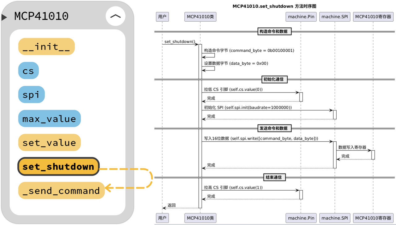
Methods inside custom MCP41010 class:
__init__ method Initialize CS pin as output and drive it high (chip deselected by default). Configure SPI with baud rate 1 MHz, polarity 0 (clock idle low), phase 0 (sample data on rising edge). Assign max_value defaulting to 255.
_send_command method Implements 16‑bit SPI transmission (command byte + data byte). Pull CS low, re‑init SPI to 1 MHz baud rate (guarantees correct speed when bus is shared with other devices), send two‑byte packet, pull CS high to terminate transfer.
Both set_value (wiper‑value programming) and set_shutdown (shutdown mode) are built upon calling _send_command.
set_value method Validate input wiper value within 0 … max_value. Build command byte 0b00010001, invoke _send_command passing command byte and wiper‑setting data byte.
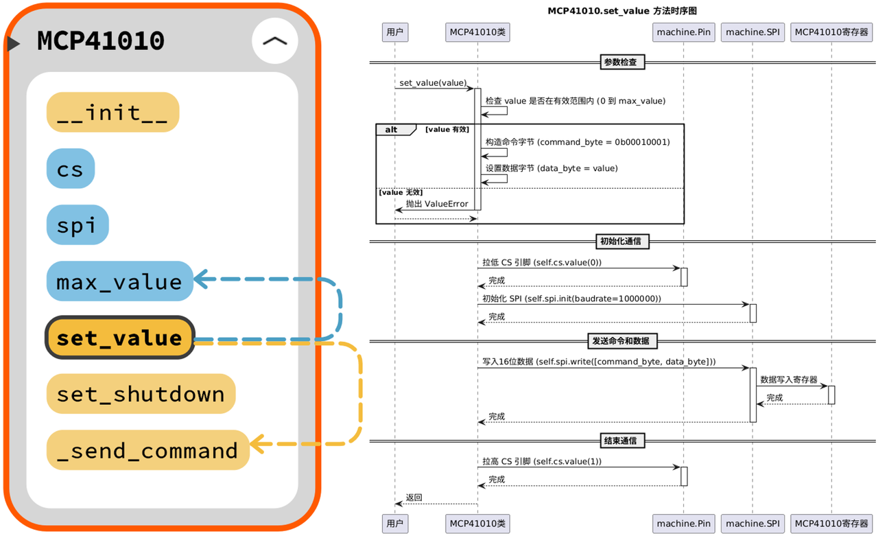
set_shutdown method Construct shutdown‑mode command byte 0b00100001, set data byte as don’t‑care 0x00, invoke _send_command.
- Waveform Generator Using AD9833
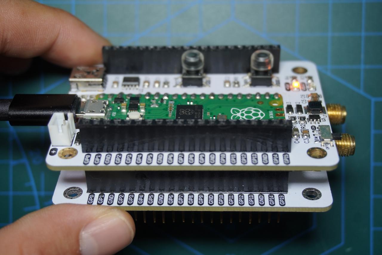
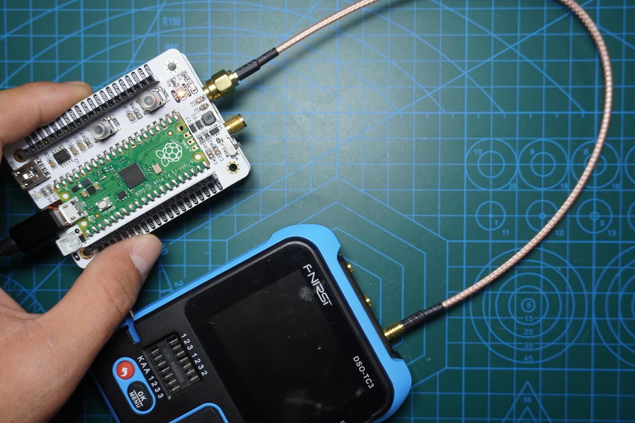
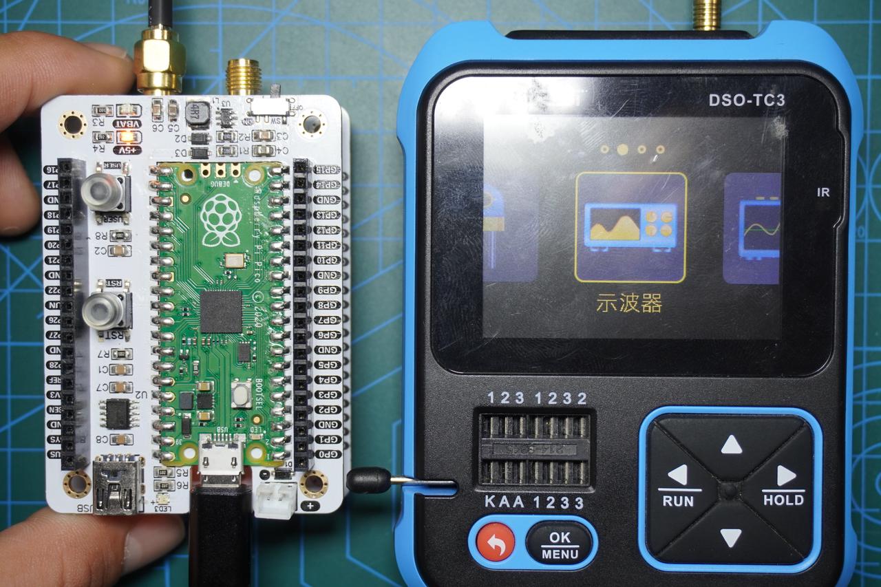
For this experiment, insert Elegance‑One Adjustable DDS Signal‑Generator Board onto Elegance‑One Universal Compatible Expansion Board. Turn on CS, SYNC, MOSI and MOSI switches of the SWITCH DIP switch on the DDS board.
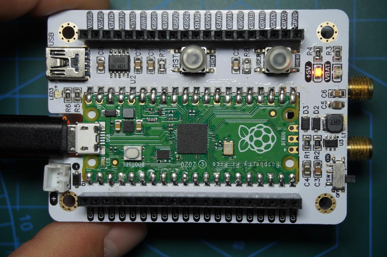
On the Elegance‑One Adjustable DDS Signal‑Generator Board, AD9833 section includes a π‑type LC power‑supply filter circuit. DDS output feeds into MCP41010 digital potentiometer acting as voltage divider. Divider output connects to a 6‑times non‑inverting amplifier producing AMPOUT amplified output. Schematic:
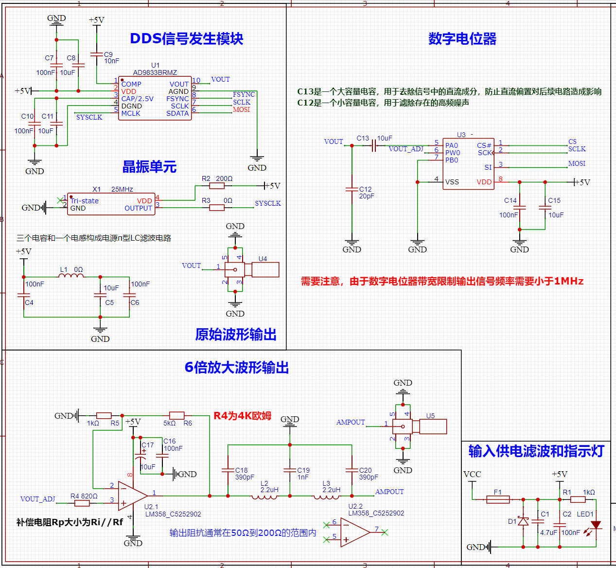
The amplified signal output path also contains a 5‑th‑order low‑pass filter with 5.43 MHz cutoff frequency. It suppresses high‑frequency spurious components and improves signal quality for high‑precision low‑noise test‑bench applications.
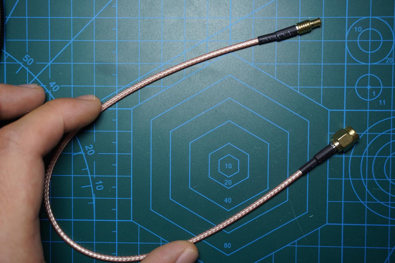
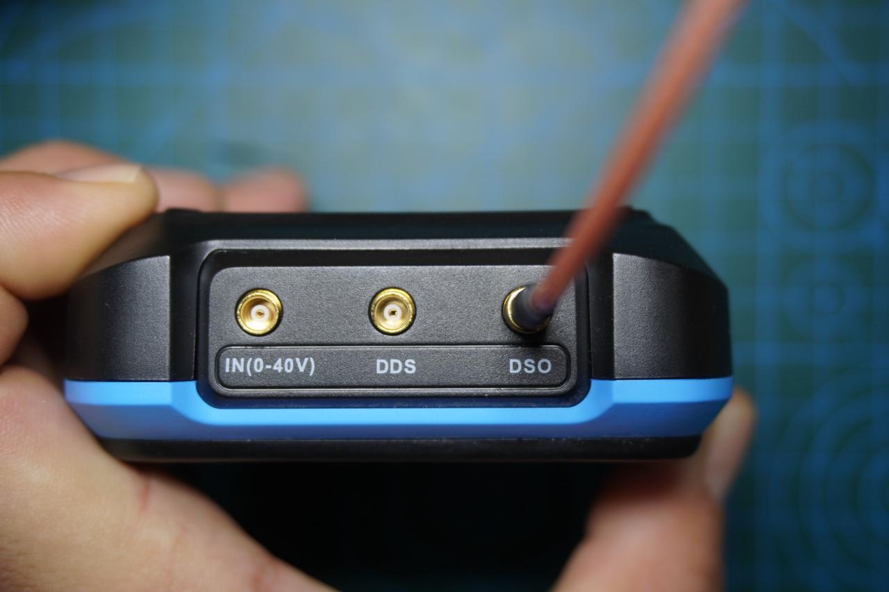
Connect the AMPOUT SMA port on the Elegance‑One Adjustable DDS Signal‑Generator Board to oscilloscope DSO MCX input port with SMA‑to‑MCX RF cable.
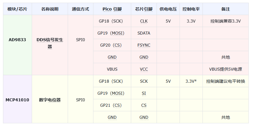
Component‑wiring table:
Save AD9833 and MCP41010 custom‑class source files as ad9833.py and mcp41010.py.
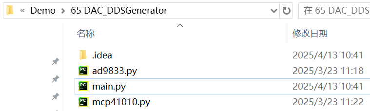
Source files are located in resource‑package path elegance‑devkit v1\Demo\64 DAC_Digipot.
The example below runs on Raspberry‑Pi Pico, uses AD9833 to generate DDS signals with configurable frequency‑and‑phase and uses MCP41010 to adjust signal amplitude.
# Python env   : MicroPython v1.23.0
# -*- coding: utf-8 -*-
# @Time    : 2024/11/4 8:52 PM
# @Author  : Li Qingshui
# @File    : main.py
# @Description : DDS signal generator using AD9833 and MCP4725 with adjustable amplitude, phase and frequency
# ======================================== Import related modules =========================================
# Import hardware‑related modules
from machine import I2C, Pin
# Import time‑related modules
import time
# Import AD9833 driver
from ad9833 import AD9833
# Import MCP41010 driver
from mcp41010 import MCP41010
# ======================================== Global variables ============================================
# ======================================== Function definitions ============================================
# ======================================== Custom classes ============================================
# ======================================== Initialization ==========================================
# 3‑second power‑on delay
time.sleep(3)
# Print debug message
print("FreakStudio: Using AD9833 and DS3502 to implement DDS signal generator")
# Create AD9833 instance on SPI0 peripheral: MOSI‑GP19, SCLK‑GP18, CS‑GP20
ad9833 = AD9833(sdo=19, clk=18, cs=20, fmclk=25, spi_id=0)
# Create MCP41010 instance on SPI0 peripheral: MOSI‑GP19, SCLK‑GP18, CS‑GP21
mcp41010 = MCP41010(clk_pin=18, cs_pin=21, mosi_pin=19, spi_id=0, max_value=255)
# ======================================== Main program ===========================================
# Configure frequency and phase for AD9833
# Program frequency‑register‑0 and phase‑register‑0
ad9833.set_frequency(5000,0)
ad9833.set_phase(0, 0, rads = False)
# Program frequency‑register‑1 and phase‑register‑1
ad9833.set_frequency(1300, 1)
ad9833.set_phase(180, 1, rads = False)
# Select active frequency‑register‑0 and phase‑register‑0
ad9833.select_freq_phase(0, 0)
# Set MCP41010 wiper value
mcp41010.set_value(125)
# Select register‑0 pair and set output waveform to sine wave
ad9833.select_freq_phase(0,0)
ad9833.set_mode('SIN')

# Adjust potentiometer value to observe DDS output waveform
# mcp41010.set_value(20)
#
# # Select register‑0 pair, output square wave
# ad9833.select_freq_phase(0,0)
# ad9833.set_mode('SQUARE')
#
# # Select register‑0 pair, output divide‑by‑2 square wave
# ad9833.select_freq_phase(0,0)
# ad9833.set_mode('SQUARE/2')
#
# # Select register‑0 pair, output triangle wave
# ad9833.select_freq_phase(0,0)
# ad9833.set_mode('TRIANGLE')
#
# # Select register‑1 pair, output triangle wave
# ad9833.select_freq_phase(1,1)
# ad9833.set_mode('TRIANGLE')
Workflow: initialize AD9833 and MCP41010 chips, then configure two frequency registers and two phase registers: Register 0: 5 kHz, 0° phase. Register 1: 1.3 kHz, 180° phase. Set MCP41010 wiper to mid‑scale value (125/255) to control analog‑signal amplitude. Select register‑0 pair on AD9833 and enable sine‑wave output.
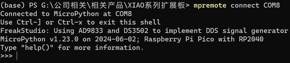
After flashing firmware, terminal output example:
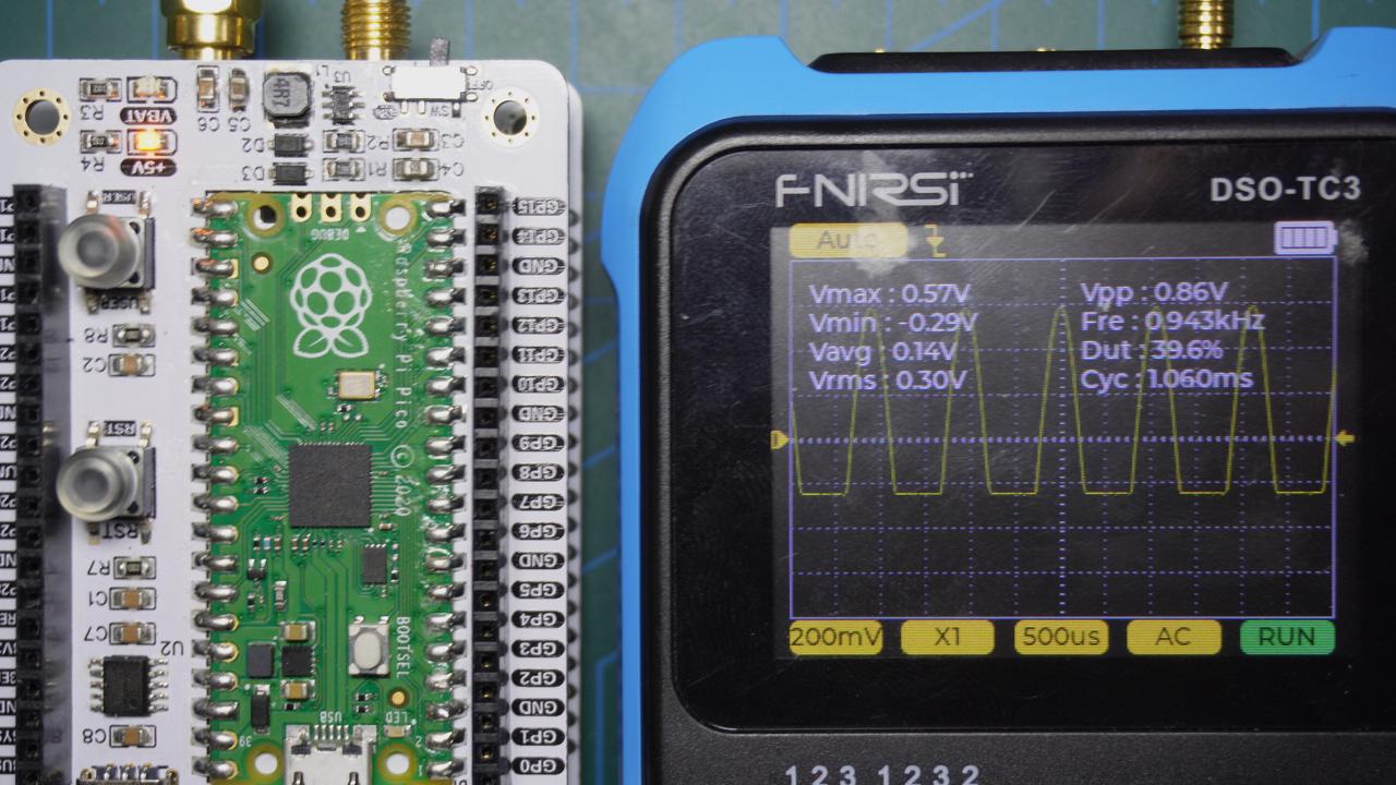
Sine‑wave output can be observed. Note that AD9833 is a single‑supply DDS chip; its output waveform is not symmetric around zero volts.
Execute mcp41010.set_value(20) command to lower potentiometer setting and reduce signal amplitude:

Output‑waveform amplitude decreases accordingly:
You can un‑comment and execute remaining lines one‑by‑one in REPL console to produce square wave, divide‑by‑two square wave and triangle wave in sequence.