Mechanical‑to‑Digital: DS3502 Solves Potentiometer Accuracy, Drift & Automation Issues
DS3502 solves mechanical potentiometer drawbacks
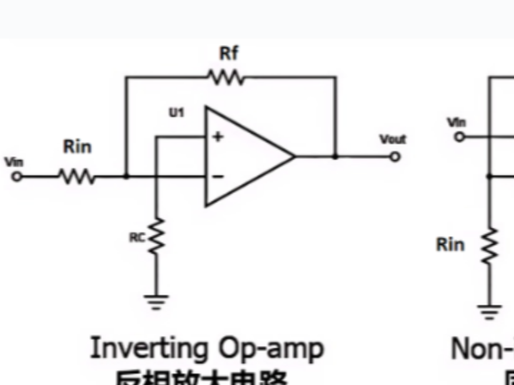
As mentioned earlier, the AD9833 chip outputs sine‑wave and triangle‑wave signals with amplitude ranging from 38 mV to 650 mV. When larger‑amplitude sine‑wave or triangle‑wave signals are required, operational amplifiers are used for amplitude boosting. Two common op‑amp topologies are the non‑inverting amplifier and the inverting amplifier, as shown below:
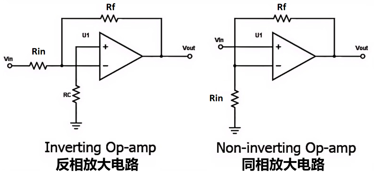
Voltage gain of non‑inverting amplifier: $$ A_v = 1 + \frac{R_f}{R_{\text{in}}} $$
Voltage gain of inverting amplifier: $$ A_v = -\frac{R_f}{R_{\text{in}}} $$
Where $R_f$ is feedback resistor and $R_{\text{in}}$ is input resistor. The non‑inverting amplifier produces output in‑phase with input signal. It features high input impedance and low output impedance and can connect directly to high‑impedance signal sources. The inverting amplifier generates output signal 180‑degrees out‑of‑phase relative to input. Its input impedance is determined by the input resistor and output impedance is low, suitable for driving low‑impedance loads.
To adjust amplifier gain, the feedback resistor $R_f$ can be replaced by a mechanical rotary potentiometer for simple and intuitive gain adjustment:
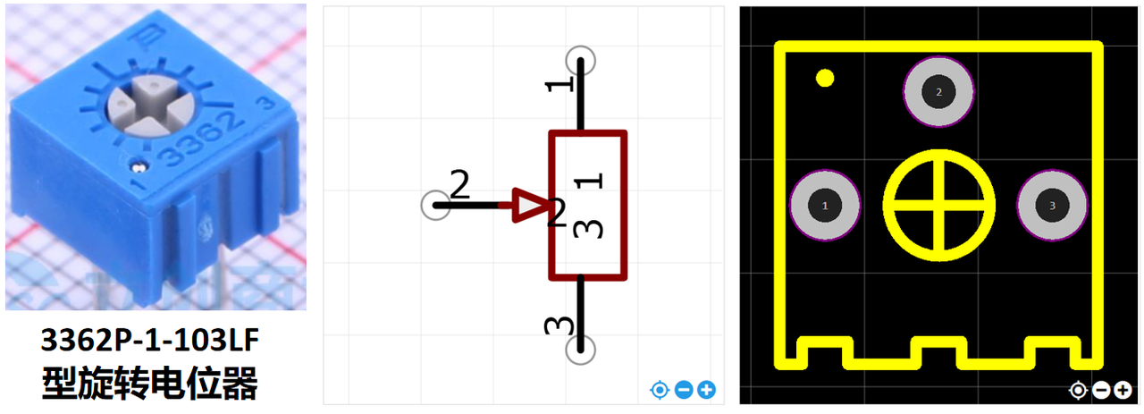
However mechanical rotary potentiometers have several drawbacks:
Susceptibility to mechanical vibration Mechanical potentiometers contain moving parts. Mechanical shock or vibration can cause unstable gain and output drift.
Low positioning accuracy Gain adjustment resolution is limited. For high‑precision signal‑conditioning circuits requiring fine trimming, mechanical markings offer poor accuracy and measurement errors easily occur.
Not suitable for automated adjustment Manual physical turning is normally required, which is incompatible with automatic or software‑controlled gain adjustment.
Wear after long‑term use Friction over time degrades mechanical components. Adjustment performance may degrade or the device can fail completely.
Digital potentiometers can replace mechanical potentiometers for amplitude adjustment. Compared with mechanical rotary potentiometers on op‑amp circuits, digital potentiometers offer these advantages:
High positioning accuracy Resistance values are controlled digitally. Each adjustment step lands precisely on predefined values, delivering high adjustment accuracy.
Immunity to mechanical vibration No moving mechanical parts. Control is purely digital. Performance is unaffected by shock, vibration or mechanical wear, delivering better stability.
Programmable adjustment for automation Digital potentiometers can be controlled by microcontrollers or computers, making them ideal for automated systems, semi‑automatic tuning and remote‑control applications.
In addition, digital potentiometers can mimic DAC functionality. Inside low‑frequency signal‑generation circuits they adjust waveform amplitude to create simple analog outputs.
This section covers two digital‑potentiometer chips with different communication interfaces:
MCP41010 SPI interface, requires three signal lines (SCK, MOSI, CS). Well‑suited for amplitude‑control together with AD9833. Reasons for selection: AD9833 itself uses SPI for configuration. MCP41010 can share the same SPI bus with AD9833. Only an extra chip‑select (CS) GPIO pin is needed, saving GPIO resources. High SPI clock rate (typical 10 MHz). Resistance values update quickly for fast response. 8‑bit resolution (256 taps). Fine adjustment steps for high‑precision amplitude‑control scenarios.
DS3502 I2C interface, requires two signal lines (SDA, SCL). Suitable for multi‑I2C‑device systems where high resolution is not mandatory: 7‑bit resolution, sufficient for basic voltage / current adjustment such as LED dimming applications. Multiple devices can share one I2C bus via configurable I2C addresses (four possible addresses). I2C consumes very little power in idle state. Good for multi‑potentiometer systems such as multi‑channel audio equalizers and battery‑powered portable equipment.
Select according to actual application requirements.
- DS3502 Digital Potentiometer Chip
1.1 DS3502 Introduction
DS3502 is a 7‑bit digital potentiometer. A microcontroller communicates over the I2C bus to set its resistance value. It provides 128 tap‑point resistance levels and operates from 2.7 V to 5.5 V supply voltage.
DS3502 supports I2C clock speeds up to 400 kHz. Maximum end‑to‑end resistance equals 10 kΩ. Two address‑select pins allow up to four DS3502 devices on a single I2C bus. It also integrates EEPROM to store the 7‑bit wiper setting across power cycles.
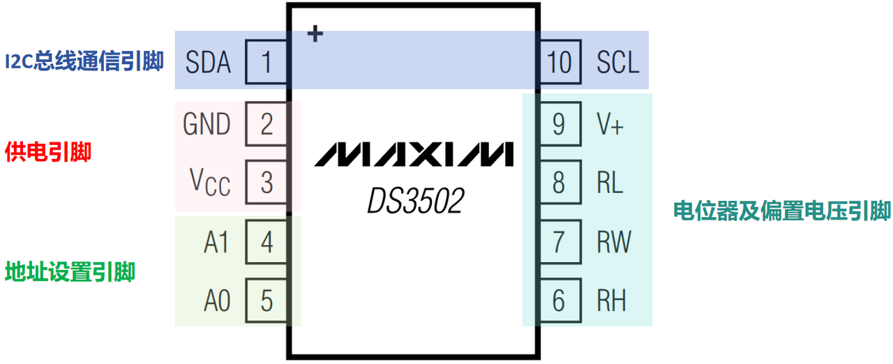
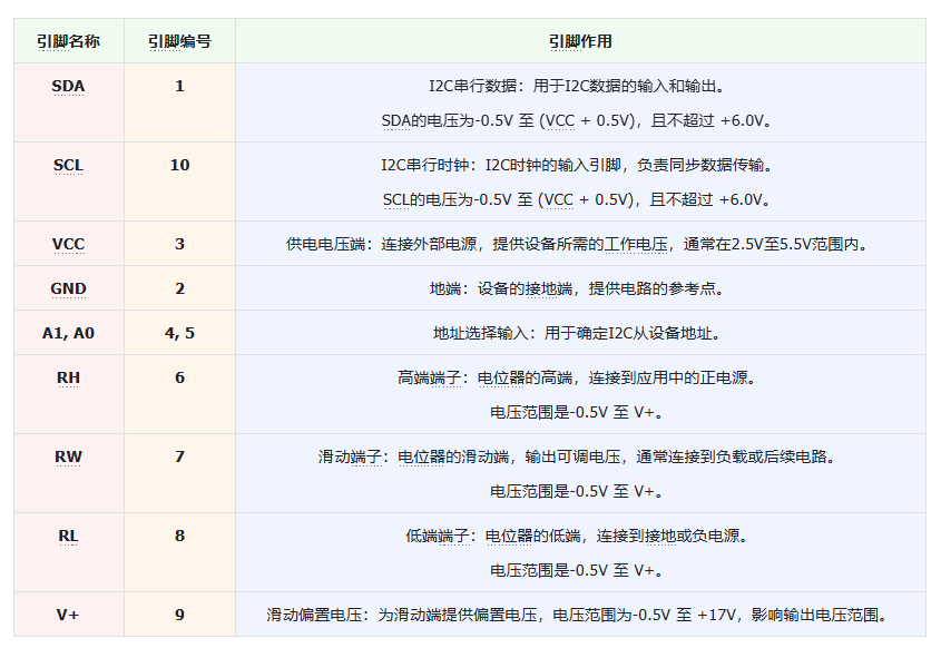
DS3502 pin assignments and functions:
1.2 DS3502 Internal Structure and Operating Principle
DS3502 internal block diagram. Core blocks include I2C interface, control register, wiper register and resistor ladder network:
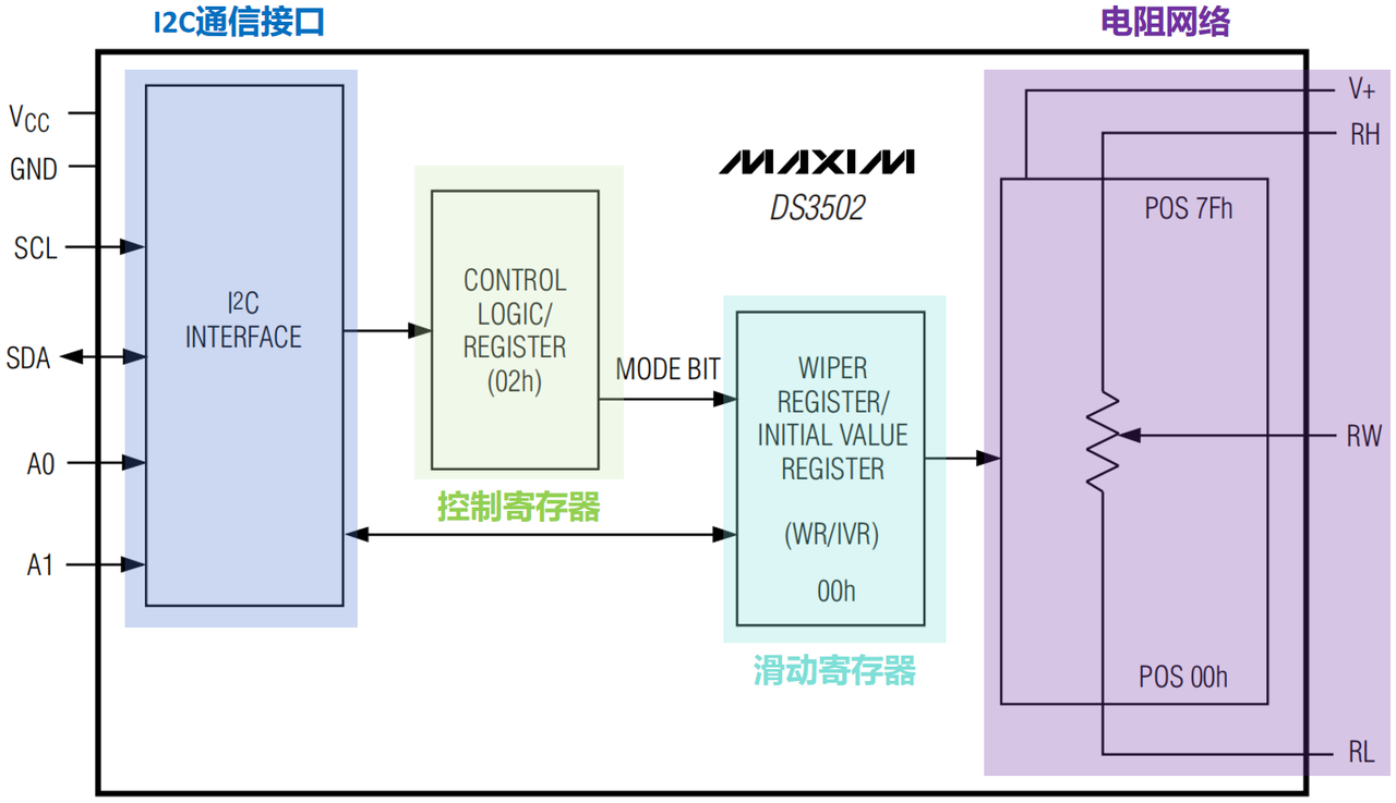
Wiper position is controlled by the Wiper Register (WR). At power‑on, the Initial‑Value Register (IVR) value is loaded into WR to set the default wiper (RW) position.

The Control Register (CR) resides at address 02h. It contains the MODE bit which defines I2C write behaviour for WR and IVR registers.
MODE = 0 I2C write to address 00h writes to both WR and IVR (CR = 00h). I2C read from address 00h returns WR content. This mode writes into EEPROM, so operations are relatively slow.
MODE = 1 I2C write to address 00h only updates WR (CR = 80h). I2C read from address 00h still returns WR content. Fast SRAM‑only write without EEPROM‑write latency.
Data inside EEPROM and SRAM are preserved when toggling the MODE bit. Power‑on default value of CR register is 00h.
The DS3502 potentiometer ladder consists of 127 series‑connected resistors between RH and RL pins. The decimal value stored inside the Wiper Register WR (range 0‑127) is decoded to turn MOSFET switches on or off. MOSFETs act as switches to connect the wiper terminal RW to a selected tap point on the resistor ladder.
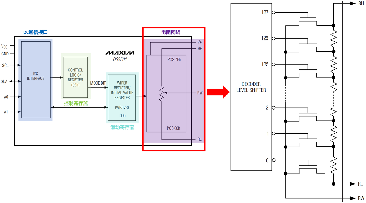
MOSFET ON Corresponding resistor segment is connected into circuit.
MOSFET OFF Tap node is disconnected from RW. Current cannot flow through that path, so that resistor segment has no effect on wiper.
Using this mechanism, adjusting WR value changes resistance seen at RW. When RH, RL and RW are wired as a voltage divider, wiper‑output voltage is calculated by: $$ V_{RW} = V_{RL} + \frac{(V_{RH} - V_{RL}) \times WR}{127} $$
Where WR is decimal wiper setting (0‑127), $V_{RL}$ is voltage at RL pin, $V_{RH}$ is voltage at RH pin.
According to DS3502 datasheet electrical characteristics, the wiper requires tWRS = 1 µs to settle after a new register value is written.
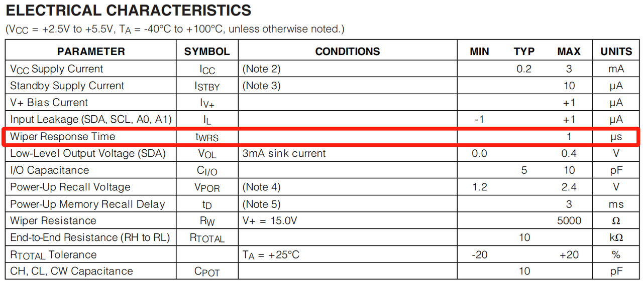
Theoretically maximum operating frequency for voltage‑divider configuration is 1 MHz ($1/t_{WRS}$).
1.3 DS3502 Communication Protocol
DS3502 I2C slave address is determined by A1 and A0 hardware pins:
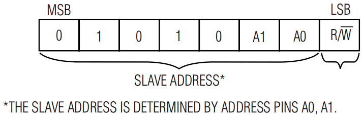
Single‑byte write sequence from microcontroller to DS3502 (example A0 and AI tied to GND): transmit slave address byte, register‑address byte, data byte:

Example communication flow for writing to WR register:

When CR.MODE = 0, writing touches EEPROM and requires completion time. Host can poll DS3502 by repeated address‑access to detect ACK response, or wait for maximum EEPROM‑write duration $t_W$ = 20 ms as specified in datasheet.

Single‑byte read example, reading CR control‑register value:
- Send slave‑address byte with R/W bit = 0 (dummy write), slave returns ACK.
- Transmit target register address
02h, slave returns ACK. - Generate Repeated‑START condition to keep bus connection active.
- Send slave‑address byte with R/W bit = 1 to signal read operation.
- Slave returns one‑byte register content. Master sends NACK to terminate transfer and generates STOP condition.
Hardware usage notes for DS3502: Place 0.01 µF and 0.1 µF decoupling capacitors on VCC power pin and V+ wiper‑supply pin. Attach 4.7 kΩ pull‑up resistors to SDA and SCL lines. If RH input voltage exceeds VCC supply, V+ pin must be tied to RH or higher potential. In other words connect V+ together with RH.
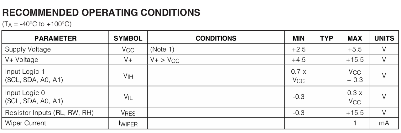
Wiper‑supply pin V+ voltage range is +4.5 V ~ 15.5 V: