MCU Memory Explained: Main Memory, External Memory & Address‑Space for Embedded Beginners
Essential embedded knowledge covering MCU main‑memory, external‑memory and address‑space system
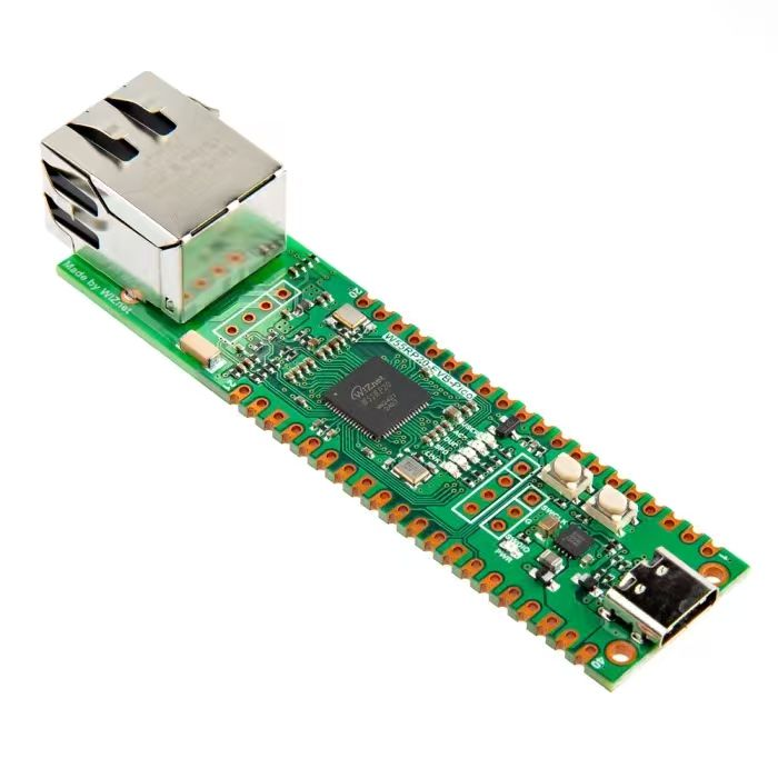
In previous lessons, we have written several MicroPython programs running on Raspberry‑Pi Pico. We used the PyCharm MicroPython plugin to upload code to the development board (flash the program). After upload, the MicroPython virtual machine compiles source code into byte‑code. The virtual‑machine interpreter executes byte‑code line‑by‑line and translates it into low‑level instructions to interact with MCU hardware resources.
This raises a question: Where exactly are these programs stored inside the MCU? How are they executed? We need to understand the relationship between programs and the MCU. This section first explains knowledge about program storage.
Overview of MCU Memory Architecture
Memory refers to storage space inside a microcontroller for program code and runtime data. From the perspective of direct CPU connection, MCU memory falls into two categories:
Main Memory Main Memory can be accessed quickly and directly by the CPU. It mainly stores currently‑running program code and data. Typical main‑memory types include ROM (Read‑Only Memory) and RAM (Random‑Access Memory). Both ROM and RAM store programs and data. ROM normally holds fixed program code, while RAM stores runtime data and variable program content.
External Memory External Memory generally refers to storage devices not directly connected to the CPU, such as data storage media accessed over USB, UART or parallel interfaces. It holds programs or data that have not yet been executed. Data from external memory must first be loaded into main memory before the CPU can run it.
- Categories and characteristics of main memory
Main memory consists of these parts:
Program Memory (ROM) Stores hardened program instructions. The MCU reads and executes instructions from ROM after power‑on. Most microcontrollers use Flash memory, which supports erasure and repeated program updates. Typical capacities range from several KB to hundreds of KB; high‑end MCUs may reach several MB.
Data Memory (RAM) Stores temporary runtime data and program variables. MCUs commonly use SRAM for global variables, local variables and intermediate values. SRAM offers fast read‑write speed but loses all data upon power loss. Typical MCU RAM sizes range from several hundred bytes to hundreds of KB.
Special‑Function Registers (SFR) Hold status information that controls MCU operation, including peripheral and core‑related configuration: Program Counter (PC), Stack Pointer (SP), and peripheral control registers.
General‑Purpose Register Group (GPR) These registers hold temporary data and computation results. They act as the bridge between CPU and memory.
1.1 Introduction to ROM Read‑Only Memory
ROM (Read‑Only Memory) is non‑volatile memory widely used in computers and embedded systems. Data is written during chip manufacturing or initial programming; afterwards it is mostly read‑only and cannot be easily modified. ROM preserves firmware and boot‑up program code so data survives power‑off events.
ROM is most often used for boot firmware, such as computer BIOS or embedded bootloaders. Firmware is a set of instructions executed before the main application, responsible for hardware initialization and loading operating‑system or application software. In embedded devices, ROM often stores operating‑system or control firmware.
Early Mask‑ROM burned data via physical masks during silicon fabrication; content could never be changed after manufacturing, requiring full chip re‑fabrication for program updates. Next came PROM (Programmable Read‑Only Memory), which allowed one‑time programming after chip delivery. Once written incorrectly or requiring modification, the chip had to be replaced. PROM was used for development‑phase testing and small‑batch production.
Today two main erasable‑reprogrammable ROM variants are common in embedded development:
EEPROM (Electrically Erasable Programmable Read‑Only Memory) Supports selective erasure and modification of individual storage cells without erasing the entire chip. Suitable for configuration data that requires occasional updates.
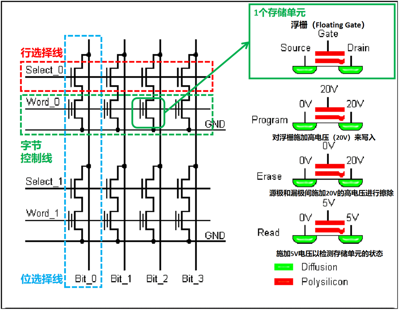
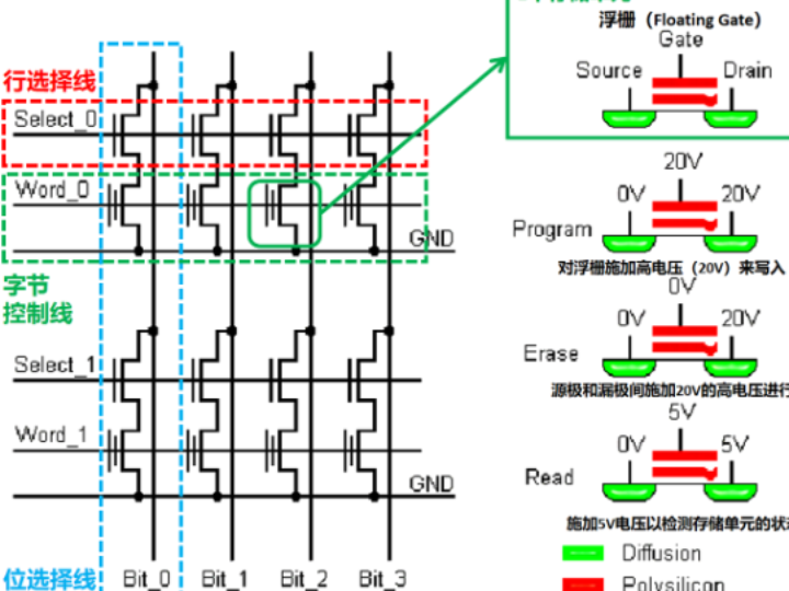
EEPROM memory‑cell array diagram. Select_x row‑select lines and Word_x word‑select lines pick individual memory cells. Each cell corresponds to one transistor storing one bit. Data is retained by trapping electrons inside the Floating Gate. Different voltages applied to byte‑operation lines perform byte‑level write, erase and read operations.
EEPROM supports byte‑level erase or page‑level erase. A page holds multiple bytes depending on device design. Single‑byte or full‑page erasure is permitted. Write operations are normally byte‑oriented. Write speed is slower than read. Write cycles consume device lifetime: typical EEPROM endurance ranges from 100 000 to 1 000 000 erase‑write cycles. Each write operation takes millisecond‑scale time. The chip enters a write‑delay state and cannot accept new operations while writing.
Flash Memory Flash Memory is a ROM type derived from EEPROM technology. It supports fast bulk erasure and reprogramming, provides high‑density storage and fast erase‑write performance. It can dynamically modify data during runtime. Flash is used both as mass‑storage (SSD, USB flash drives) and as program memory inside embedded MCUs.
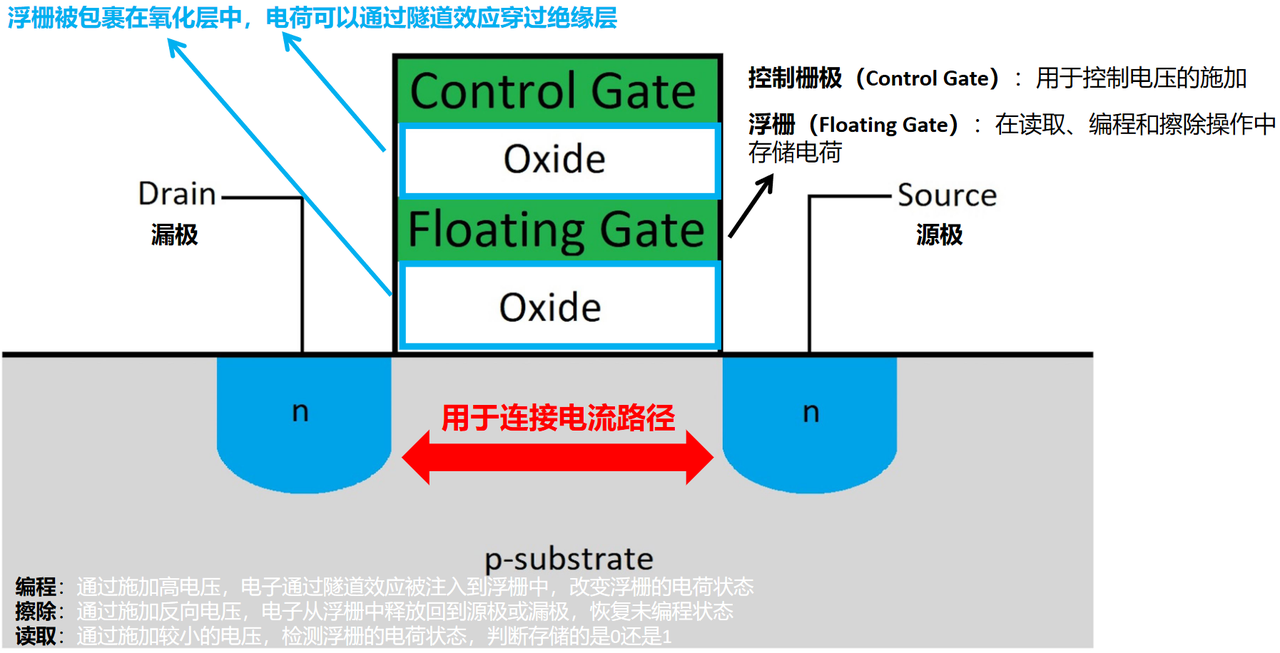
The core building block of Flash Memory is the Floating‑Gate Transistor, whose operating principle resembles EEPROM.
Flash Memory performs erase operations in Block or Sector units; block / sector size ranges from several KB to several MB. An erase cycle must run before writing new content. Write (program) operations execute in Page units; page sizes range from hundreds of bytes to several KB. Flash has limited erase‑write endurance, typically 10 000‑100 000 cycles. Block erase takes several to tens of milliseconds; programming takes hundreds of microseconds to several milliseconds. Flash is divided into two major architectures:
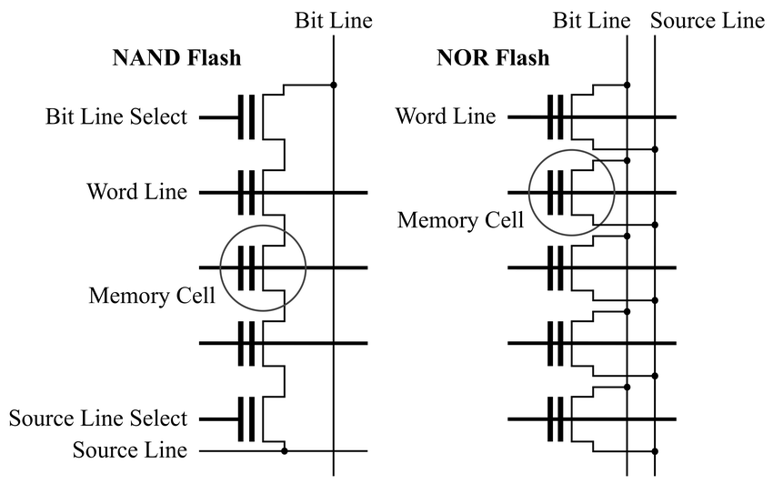
NAND Flash memory‑cells are connected in series, multiple cells share the same bit‑line. NOR Flash has no separate bit‑line selection circuit; each memory‑cell connects directly to bit‑line and source‑line for direct cell access.
NOR Flash Uses linear addressing architecture. Memory cells are byte‑addressable similar to traditional RAM; every byte has an independent address. It supports direct random byte reads. Thanks to linear addressing it supports XIP (Execute‑In‑Place), so it is widely used for firmware and program‑code storage requiring high read performance. NOR Flash delivers fast read speed, yet erase‑write operations are relatively slow. Storage density is low, suited for small‑capacity storage from several MB up to tens of MB. Unit cell area is large, leading to higher manufacturing cost.
NAND Flash Uses matrix‑based addressing. Data is organized in pages and blocks. Read‑write happens mostly in page units; erase operates on block boundaries. It cannot perform true random byte reads like NOR Flash; access is sequential large‑block oriented. NAND Flash achieves excellent speed for sequential read‑write of large data blocks, while random‑read performance is poorer. It features high storage density and is deployed for high‑capacity storage such as SSD and USB mass‑storage drives.
Differences between EEPROM pages and Flash sectors, despite both being segmented storage management:
Write method: EEPROM pages support byte‑level writes, single‑byte updates are often possible without full‑page erasure. Flash sectors must erase the whole sector before any write operation.
Storage structure: EEPROM consists of consecutive pages of fixed size e.g. 64 bytes. Flash sectors are usually larger e.g. 4 KB, 16 KB and each sector contains multiple pages.
1.2 Introduction to RAM Random‑Access Memory
RAM (Random‑Access Memory) is a key storage medium in computers and embedded hardware. It permits reading and writing in arbitrary order. It provides fast‑access data storage for processors to run application code and schedule operating‑system tasks. RAM is volatile; all data is lost upon power loss.
Simplified RAM architecture diagram. Read‑write control signals select read or write operation. Address decoders drive word‑line and bit‑line signals to pick target memory rows or cells. Data input‑output circuitry handles incoming and outgoing data streams. Memory cells are latches holding state until refreshed or overwritten.
Based on internal working principle RAM is split into two families:
DRAM (Dynamic Random‑Access Memory) Each DRAM memory‑cell consists of one capacitor plus one transistor. Capacitor charge level represents binary state: charged for logic‑1, discharged for logic‑0. The transistor acts as switch controlling charge and discharge. Cells are arranged in two‑dimensional matrices of word‑lines and bit‑lines. Writing injects or drains charge via transistors. Reading samples capacitor charge level; reading consumes stored charge so a refresh must follow read operations.
Simplified DRAM diagram. Data is stored as capacitor charge, accessed via switching transistors. Hierarchical organization includes Rank, Bank, MAT and other layers connected by local and global bit‑lines and word‑lines. During read operations row decoders activate target rows, sense amplifiers resolve tiny charge differences into binary values.
Capacitors leak charge over time, requiring periodic refresh cycles every few milliseconds to preserve data integrity. This refresh requirement gives DRAM its "dynamic" name. Refresh reads cell content and writes it back.
SRAM (Static Random‑Access Memory) Each SRAM memory‑cell uses six transistors: two cross‑coupled inverters for latching binary state (1 / 0), plus two access transistors controlling read‑write operations. Cells are laid‑out as two‑dimensional matrices. Unlike DRAM, cross‑coupled inverters form stable feedback states and no refresh is needed.
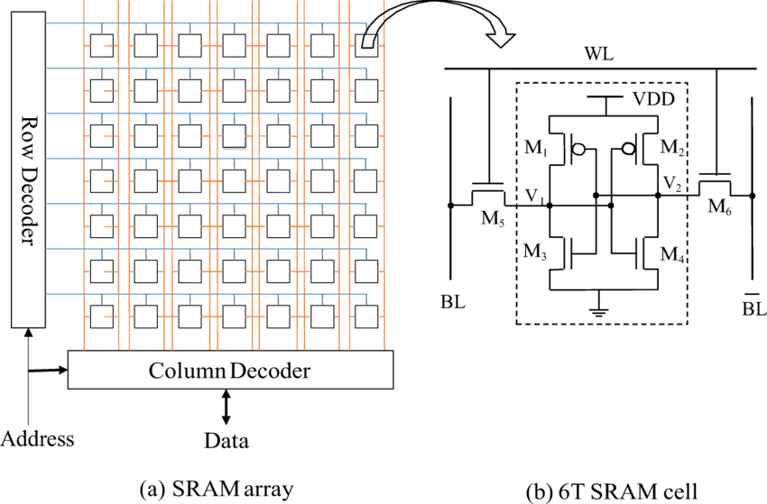
Each inverter is built from a transistor‑pair; four transistors maintain stored bit state. For writes the word‑line goes high enabling access transistors; data is driven onto bit‑lines BL and BLB into inverters. For reads the word‑line enables access transistors; bit‑line voltages reflect the stored bit value and are decoded by sense amplifiers.
Because refresh cycles are eliminated SRAM delivers much faster read‑write performance, suitable for high‑speed scenarios. However the six‑transistor cell reduces storage density and increases per‑bit cost compared with DRAM.
- Categories and characteristics of external memory
Common external‑memory types include external RAM, external ROM, external EEPROM and memory cards.
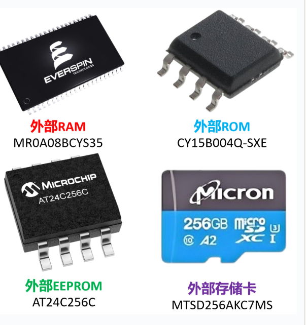
Different external‑memory types feature distinct properties and application scenarios.
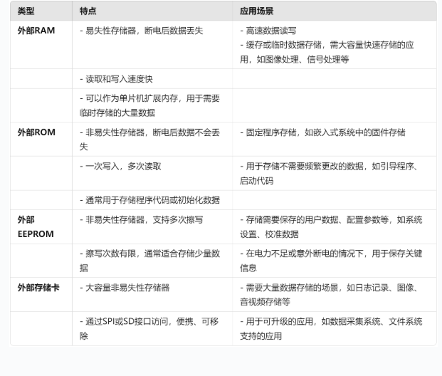
- Address space and bus architecture
Address space is the full range of memory locations directly accessible by an MCU. Every memory location has a unique hexadecimal address. For example the RP2040 inside Raspberry‑Pi Pico is a 32‑bit microcontroller. Its address space is 32‑bit wide, giving 2^32 unique addresses, equal to 4 294 967 296 bytes (~4 GB), ranging from 0x00000000 to 0xFFFFFFFF.
This 4 GB address space is partitioned into functional regions including ROM, SRAM, peripherals and XIP (Execute‑In‑Place). Address ranges map to different memory blocks and peripherals so developers can manipulate hardware resources directly.
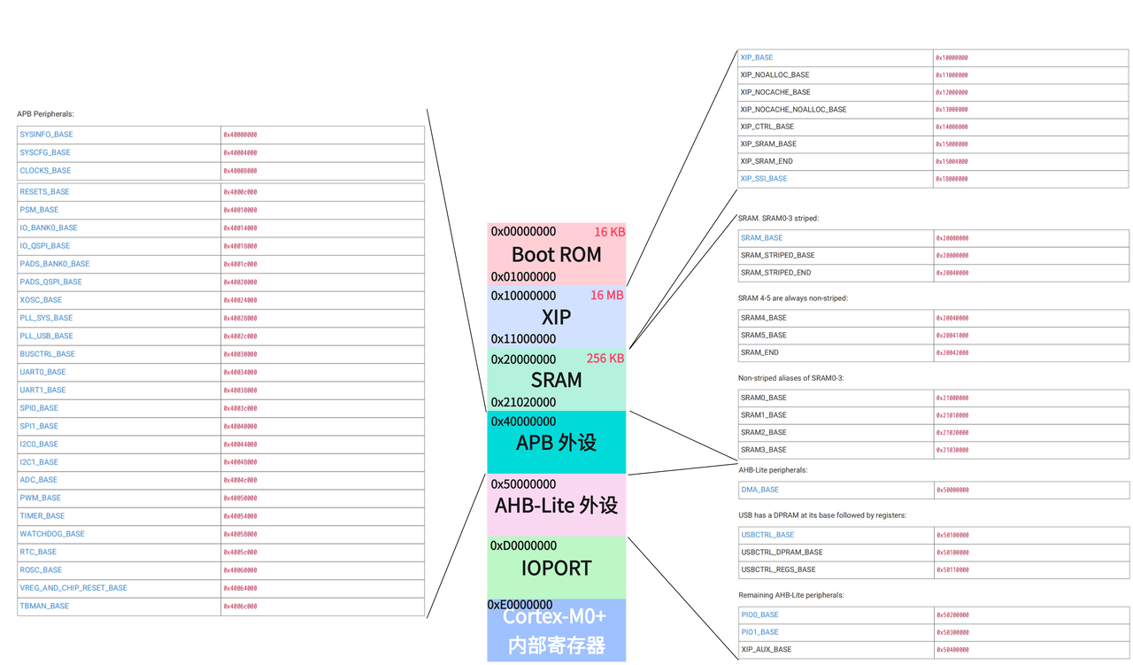
Major partitions:
Boot ROM (Read‑Only Memory) Upon power‑on or reset RP2040 first executes boot code from Boot‑ROM, responsible for hardware initialization and launching user application code.
XIP (Execute‑In‑Place register region) XIP maps external QSPI Flash memory, holding user program and data. XIP permits RP2040 to fetch and execute code directly from Flash without copying code into RAM. RP2040 communicates with external Flash over the QSPI bus.
SRAM (Static Random‑Access Memory) Stores runtime temporary variables, stack and intermediate program data.
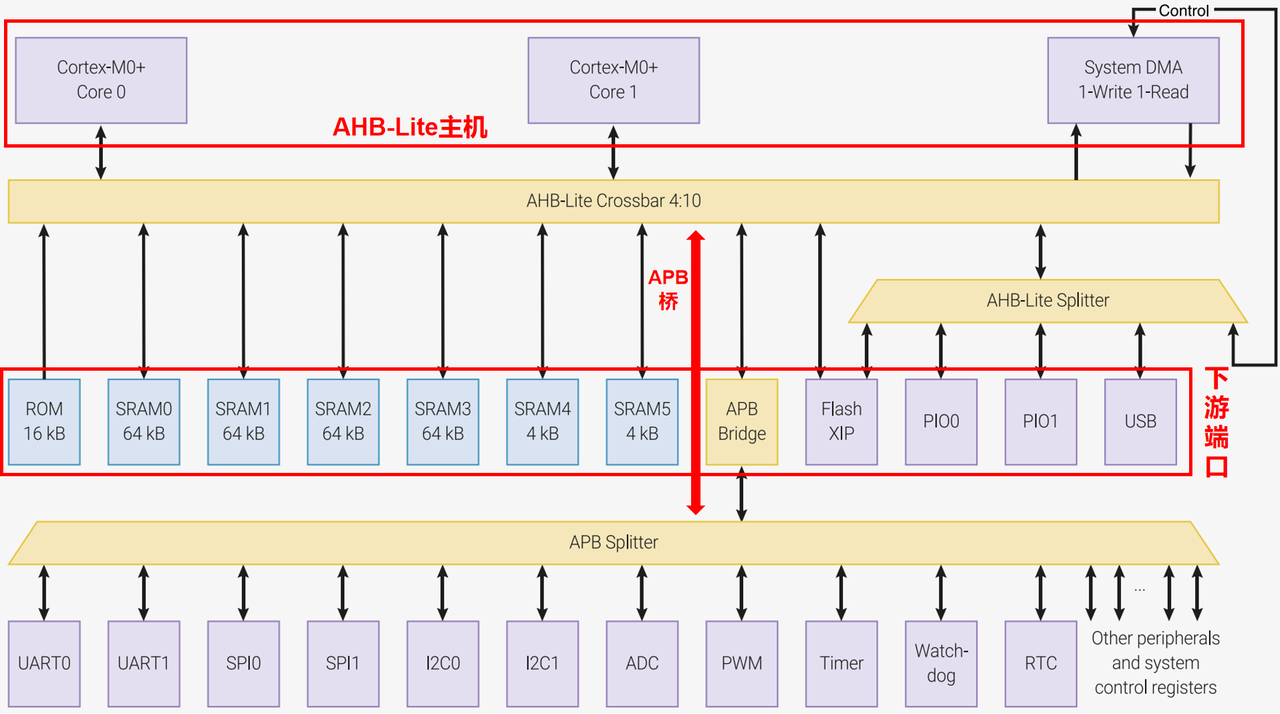
APB Peripherals (low‑speed peripheral bus) Connects low‑bandwidth peripherals such as GPIO controllers, timers and ADC. APB peripherals are controlled by reading‑writing memory‑mapped registers.
AHB‑Lite Peripherals (high‑speed peripheral bus) Register mapping for high‑throughput peripherals including DMA controller, USB controller and PIO (Programmable Input‑Output). These units handle high‑volume data transfers.
IOPORT (Input‑Output port registers) Contains SIO (Single‑cycle Input‑Output) registers for fast manipulation of GPIO pins and simple peripherals.
Cortex‑M0+ internal registers Holds ARM Cortex‑M0+ core‑internal registers: interrupt controller, SysTick system timer, debug interfaces etc. These control core MCU functions such as interrupt handling and system timing.
APB and AHB‑Lite buses are communication channels interconnecting CPU, memory and peripherals (UART, SPI, I2C etc). They carry data, address and control signals. The CPU accesses bus‑mapped addresses to configure peripherals and read hardware status.