



MCP4725 Deep‑Dive: Pins, Registers, Modes & Application Circuits
MCP4725 chip full interpretation
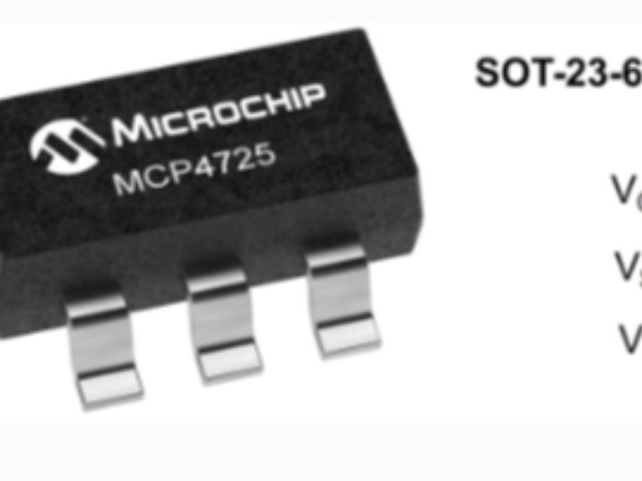
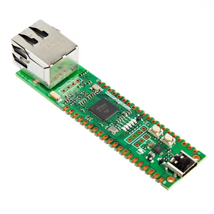
- Introduction to MCP4725
MCP4725 is a single‑channel 12‑bit Digital‑to‑Analog Converter (DAC) manufactured by Microchip. It features non‑volatile EEPROM storage. It is widely used in applications requiring precise analog output such as audio‑signal generation, sensor‑signal conditioning and voltage reference adjustment.
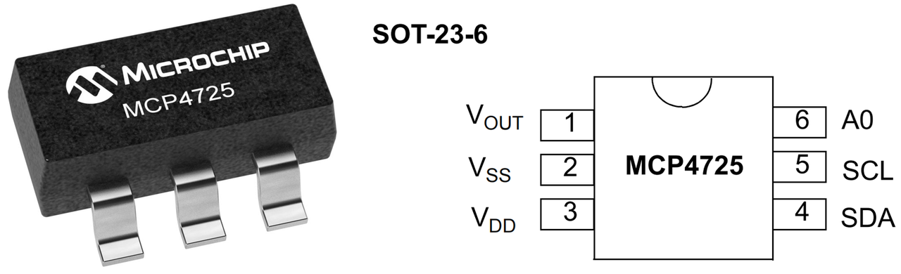
Key features of MCP4725:
12‑bit resolution MCP4725 provides 12‑bit resolution, delivering 4096 distinct output voltage levels. Suitable for high‑precision signal‑generation scenarios.
I²C interface Communication is performed over the I²C bus. Simple integration with microcontroller hosts; DAC output can be controlled via standard I²C protocol.
EEPROM storage On‑chip non‑volatile EEPROM stores DAC register values. Output settings are retained even after power‑off or system reset.
Output voltage range Output spans from 0 V to Vcc. Output accuracy depends on reference voltage Vref, which typically equals supply voltage.
Low power consumption Low‑power device well‑suited for battery‑powered applications.
Compact package Available in SOT‑23 or MSOP‑8 packages for space‑constrained hardware designs.
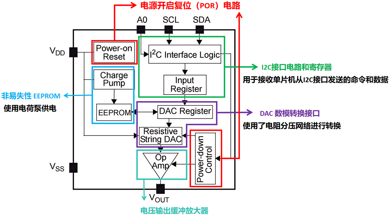
Internal block diagram:
- MCP4725 Pin‑out Description
MCP4725 pin‑function table:
- MCP4725 Electrical Characteristics
Electrical‑parameter specifications:
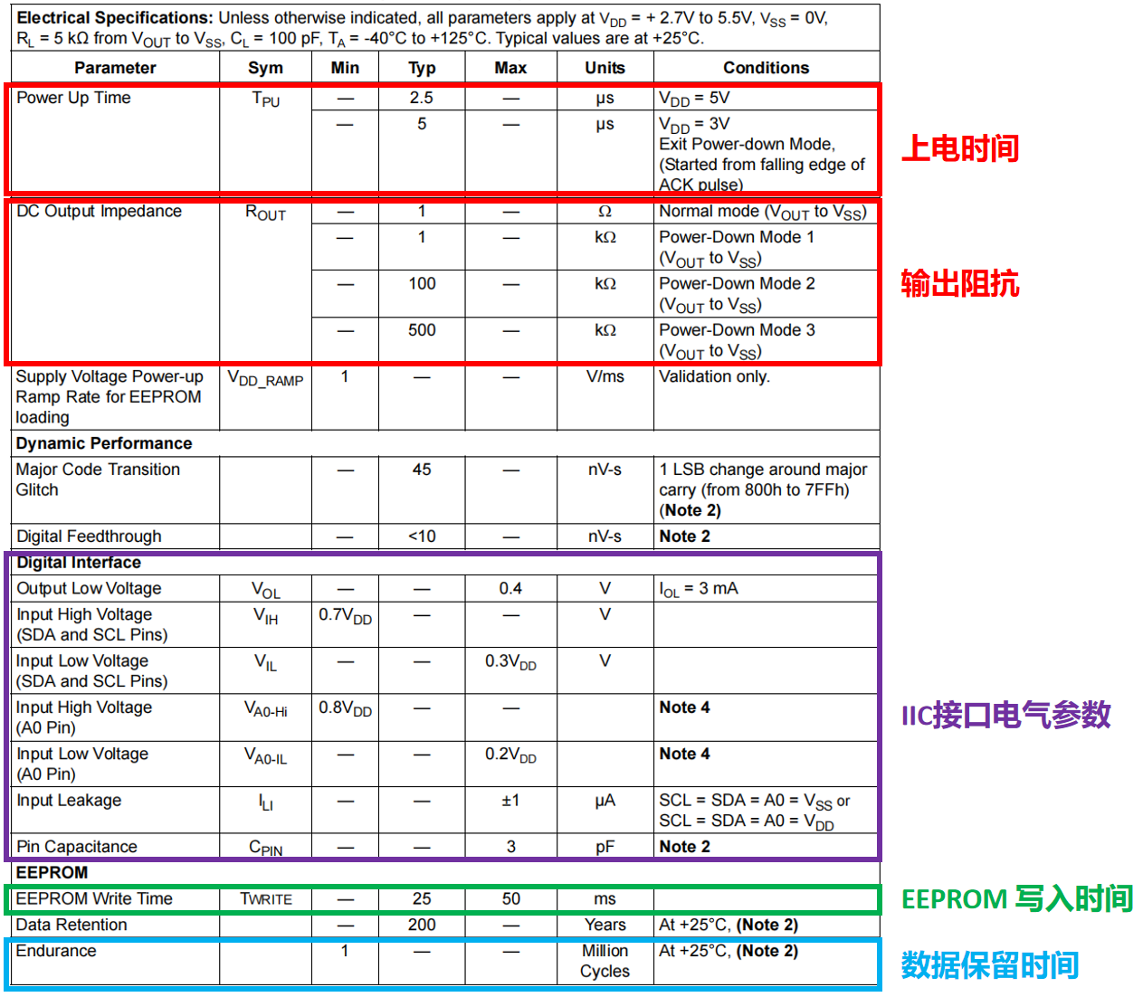
Important parameters:
Operating Voltage (VDD) Valid supply‑voltage range for normal DAC operation: 2.7 V to 5.5 V.
Supply Current (IDD) Typical active‑mode supply‑current consumption: 210 µA.
Power‑Down Current (IDDP) Typical current draw in power‑saving mode: 0.06 µA.
Integral Non‑Linearity Error (INL) Deviation between real DAC output and ideal linear transfer curve. Maximum ±14.5 LSB, quantifies output linearity. Larger INL increases deviation between real output and expected value.
Differential Non‑Linearity Error (DNL) Error between analog outputs of two consecutive digital codes. Typical ±0.2 LSB. Small DNL means even output‑voltage steps across digital‑code transitions.
Gain Error (GE) Deviation of real amplifier gain from ideal gain. Typical −0.1 % (maximum 2 %). Large gain error shifts output voltage away from expected levels.
Output Voltage Settling Time (TS) Time required for DAC output voltage to stabilize after a code change. Typical value 6 µs. Short settling time means fast response to input‑code updates.
Power‑on Time Interval from power application until device is fully ready. Short power‑on time benefits frequently‑restarting systems.
Output Resistance (ROUT) Internal resistance at DAC output pin. Low output resistance (1 Ω) in normal mode stabilizes output voltage; high impedance in power‑down mode changes output‑drive capability.
EEPROM Write Time Time consumed for EEPROM‑write operations.
Data Retention Time Period for which EEPROM preserves stored values without power supply.
- MCP4725 Operating Modes
Two operating modes are available: normal mode and power‑down mode. Mode is selected by programming the power‑down bits PD1 and PD0 inside the configuration register. These two bits can also be stored inside non‑volatile EEPROM.
Normal mode Device performs regular digital‑to‑analog conversion.
Power‑Down / Power‑Saving mode Device enters low‑power state; most internal circuits are disabled. No conversion takes place and VOUT output is de‑activated. Output stage connects to a predefined resistive load determined by PD bits. This prevents undesired output voltages during power‑up or power‑down sequences.
Power‑down bit assignments:
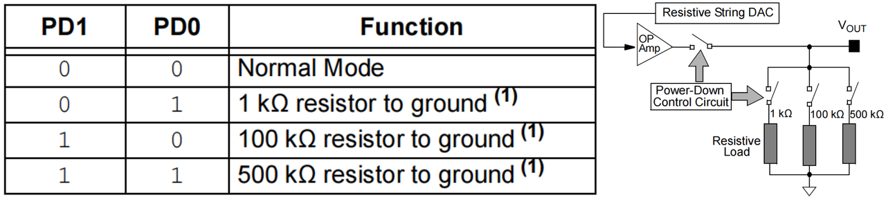
PD1 = 0, PD0 = 0, Normal mode PD1 = 0, PD0 = 1, 1 kΩ pull‑down resistor to GND PD1 = 1, PD0 = 0, 100 kΩ pull‑down resistor to GND PD1 = 0, PD0 = 1, 500 kΩ pull‑down resistor to GND
Selecting appropriate resistor values controls leakage current at output pin during power‑down state.
- MCP4725 EEPROM Storage
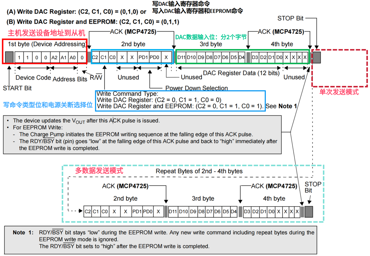
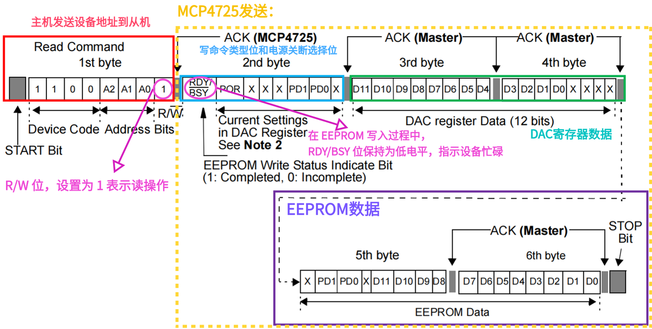
MCP4725 integrates 14‑bit EEPROM memory: 2 configuration bits plus 12‑bit DAC input data. These bits can be read or written via I²C commands. EEPROM write operation is triggered by the EEPROM‑write command (data bits C2 = 0, C1 = 1, C0 = 1). During writing, status bit RDY/BSY stays low; it goes high once writing completes. Any further write commands received while busy are ignored.
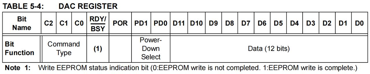
DAC register data bits
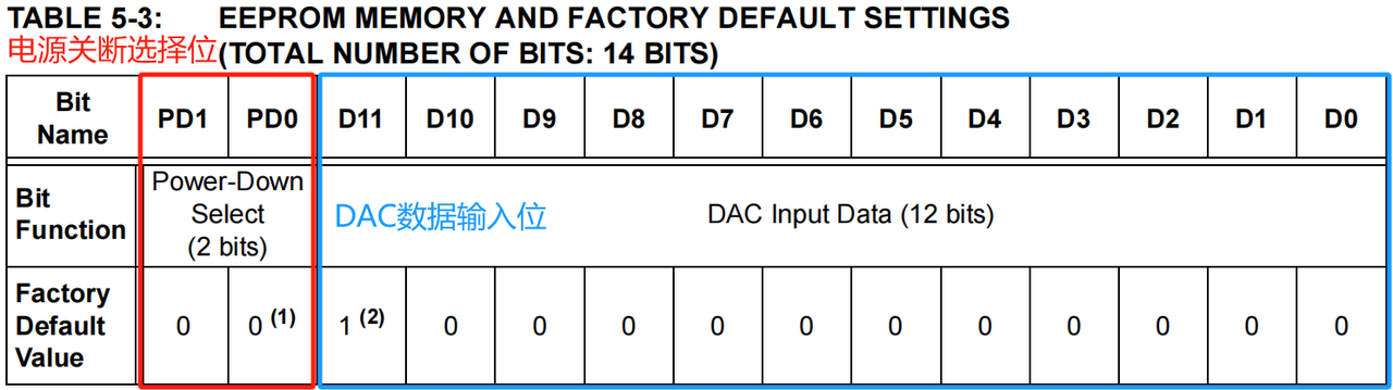
EEPROM memory layout and factory‑default values
- MCP4725 Operation
MCP4725 communicates as an I²C slave device with a host MCU. The host reads and writes the DAC input register and EEPROM using I²C commands.
The MCP4725 I²C slave address consists of four fixed bits (1100 = device identifier) plus three address bits A2, A1, A0. A2 and A1 are hard‑wired during manufacturing and default to "00". The A0 bit is determined by the logic level applied to the A0 physical pin.
Pin A0 may be tied to VDD, VSS, or driven by a digital logic signal.
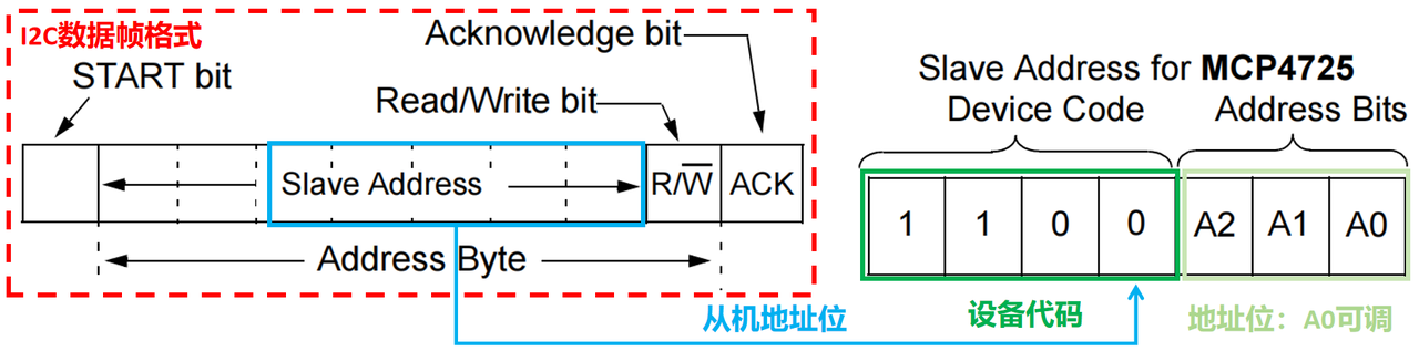
MCP4725 I²C address bit definition
6.1 MCP4725 Write Commands
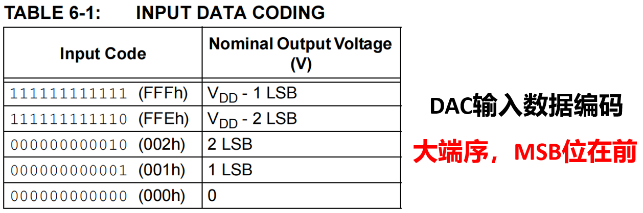
Analog‑output codes are transmitted over I²C. MCP4725 uses unsigned‑binary input codes; output voltage ranges from 0 V to VDD. Output‑voltage formula:
$$ V_{OUT} = \frac{D}{2^{12}} \times V_{DD} $$
Where D = DAC input data, ranging from 0 to 4095.
Write commands load configuration bits and DAC codes into DAC registers or write values into EEPROM. Three write‑command‑type bits (C2, C1, C0) select command function.
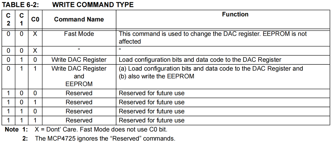
Three write‑command types:
Fast‑mode Write Command (C2=0, C1=0, C0=X) Updates only the DAC register; EEPROM content remains unchanged. Updates power‑down‑select bits (PD1, PD0) and the 12‑bit DAC input code. VOUT updates on the falling edge of the ACK pulse of the third byte. ‑ After sending three‑byte command, send STOP condition to complete single write transaction. ‑ Alternatively send Repeated‑Start after three‑byte command, then transmit new second‑byte / third‑byte data to perform multiple consecutive updates.
Write DAC Input Register Command (C2=0, C1=1, C0=0) Provides identical function as fast‑mode write, but separates command‑type / power‑down bits from DAC‑data bytes. D11‑D0 DAC data are contained inside third and fourth bytes; the four least‑significant bits of byte four are don’t‑care bits. Device executes write upon receiving fourth byte. Host may issue STOP or Repeated‑Start after transmission.
Write DAC Input Register and EEPROM Command (C2=0, C1=1, C0=1) Loads configuration and data bits into DAC register and simultaneously writes those values into EEPROM. RDY/BSY pin goes low during EEPROM programming and returns high upon completion. Host can poll RDY/BSY status via read commands.
6.2 MCP4725 Read Commands
Read operations fetch content from DAC output register and EEPROM. When host transmits address byte with R/W bit set high (R/W = 1), MCP4725 enters read mode and outputs current DAC‑register and EEPROM data onto the SDA line.
- MCP4725 I2C General‑Call and High‑Speed Mode
7.1 General Call
General Call is a special I²C broadcast mechanism. Host transmits the General‑Call address instead of addressing one specific slave. All connected slaves receive this message. MCP4725 responds to selected General‑Call commands. General‑Call address = 0x00. Command function is defined by the second data byte.
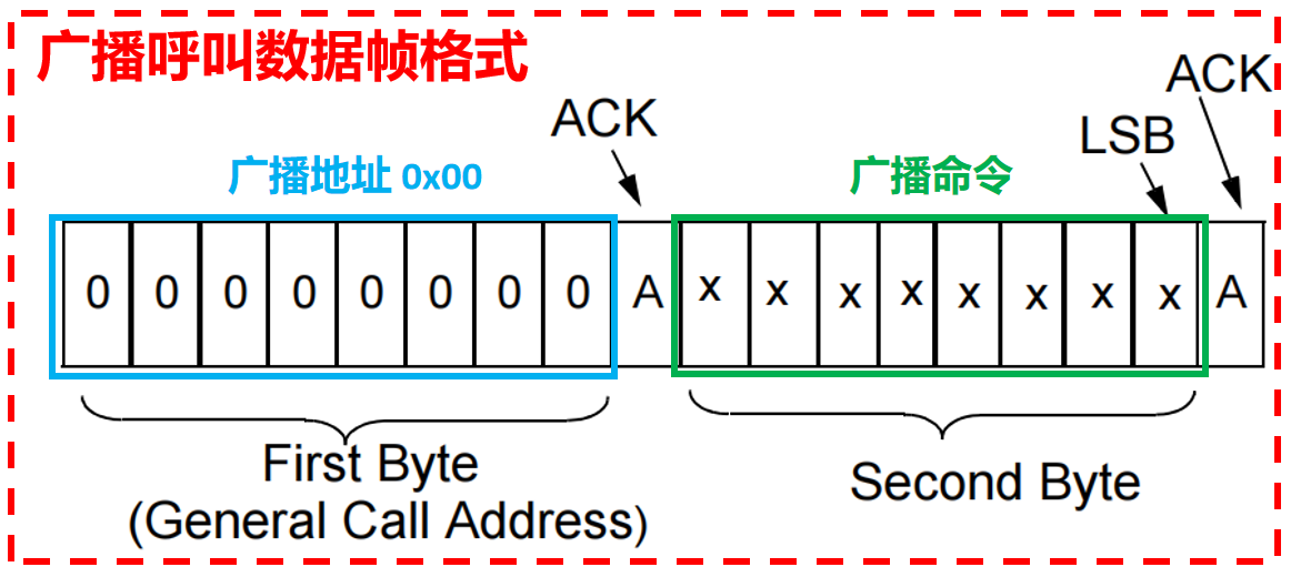
General‑Call frame format
Supported General‑Call operations:
General Call Reset Second byte = 00000110 (06h). MCP4725 aborts ongoing conversion and executes internal reset similar to power‑on reset (POR). Values stored inside EEPROM are re‑loaded into DAC registers, restoring power‑on default state.
General Call Wake‑up Second byte = 00001001 (09h). Resets PD1 / PD2 power‑down bits to normal‑mode (PD1, PD2 = 0,0). EEPROM stored power‑down settings remain untouched.
Multiple MCP4725 chips can share one I²C bus. General‑call commands allow synchronous reset or wake‑up of all devices to simplify system initialization.
7.2 High‑Speed Mode
HS Mode is one of three defined I²C operating modes for high‑throughput applications, supporting transfer speeds up to 3.4 Mbit/s, faster than standard‑mode (100 kbit/s) and fast‑mode (400 kbit/s). To enter HS Mode, host sends special address byte 00001XXX where XXX is unique HS‑master code. MCP4725 does not ACK this byte but switches into HS‑Mode operation. HS‑mode I²C reduces bus‑occupation time and improves response speed for multi‑device high‑speed communication scenarios.
- Typical MCP4725 Applications
8.1 Simple Voltage Output
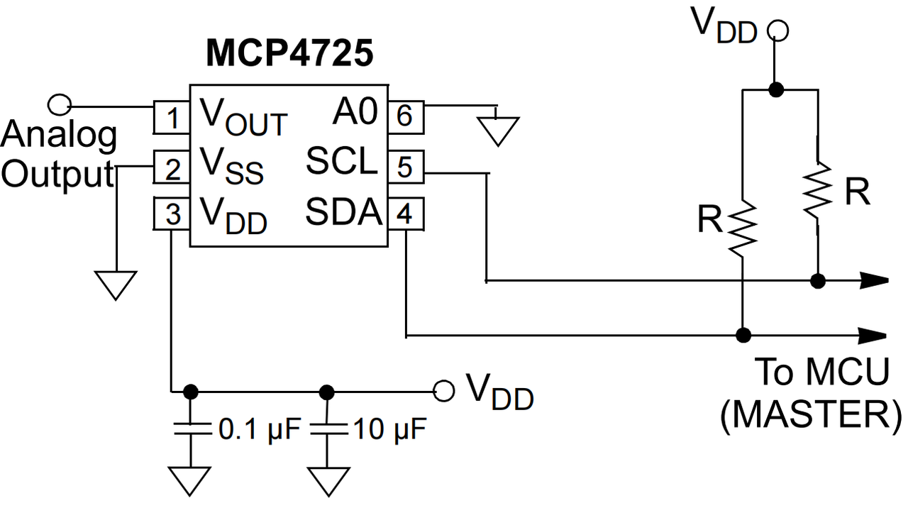
Vout is analog‑voltage output. Pin A0 can be tied to GND, VDD or a MCU digital pin to configure I²C address. Two pull‑up resistors (typically 1 kΩ ~ 10 kΩ) are attached to I²C bus lines. Power‑supply input VDD is filtered with one 10 µF tantalum capacitor plus one 0.1 µF ceramic capacitor; these capacitors should be placed within 4 mm of the VDD pin on PCB.
Schematic for simple voltage‑output circuit:
8.2 Reducing DAC Output Step Size
When VDD = 3.3 V, MCP4725 output step size equals 3.3 V / 4096 ≈ 0.805 mV. Some applications demand much smaller output steps e.g. 200 µV. A voltage‑divider network scales down DAC output amplitude and suppresses noise.
Example circuit for fine threshold adjustment in optical‑sensor detection:
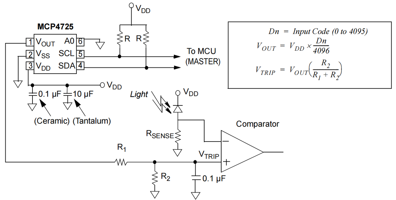
R1 and R2 form voltage divider converting DAC VOUT into lower threshold voltage VTRIP. $$ V_{TRIP} = V_{OUT} × (R2 / (R1 + R2)) $$
Comparator other input connects to sense resistor RSENSE and photodiode. RSENSE develops voltage proportional to photodiode photocurrent under illumination. Comparator compares VTRIP against RSENSE voltage to generate threshold‑detection output for light‑intensity monitoring.
8.3 Window DAC Construction
For sensor applications requiring extremely high resolution within a narrow voltage band, a divider network with pull‑up / pull‑down resistors implements a “window DAC”. It narrows effective output‑voltage swing while greatly improving step resolution.
Example circuit for over‑current detection:
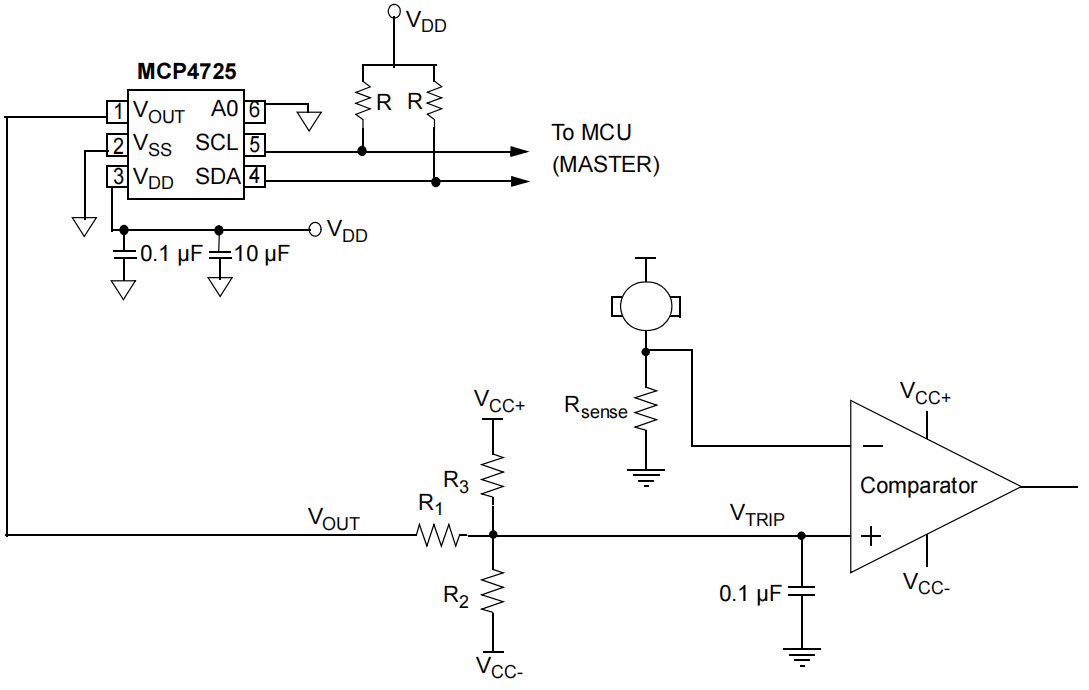
MCP4725 generates analog VOUT from digital input code Dn: $$ V_{OUT} = V_{DD} \times \frac{Dn}{2^{12}} $$
R1, R2, R3 build divider network converting VOUT into comparator threshold VTRIP. Circuit can be simplified using Thevenin equivalent formulas: $$ R_{23} = \frac{R_2 R_3}{R_2 + R_3} $$ $$ V_{23} = \frac{(V_{CC+} \times R_2) + (V_{CC-} \times R_3)}{R_2 + R_3} $$
Final comparator‑input threshold: $$ V_{TRIP} = \frac{V_{OUT} \times R_{23} + V_{23} \times R_1}{R_2 + R_{23}} $$
Current‑sense resistor Rsense measures load‑current. Comparator judges over‑current condition by comparing Rsense voltage drop against VTRIP.
8.4 Bipolar‑Voltage Output
An external operational‑amplifier circuit implements bipolar output. Resistor values set output swing, gain and noise performance. R1 / R2 configure amplifier gain; R3 / R4 set output offset level.
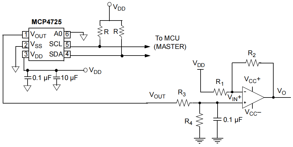
Op‑amp buffers and conditions MCP4725 output signal. $$ V_{IN+} = \frac{V_{OUT}R_4}{R_3 + R_4} $$ $$ V_O = V_{IN+} \left(1 + \frac{R_2}{R_1}\right) - V_{DD}\left(\frac{R_2}{R_1}\right) $$
For larger offset levels, connect R4 to VDD instead of VSS and use pull‑up resistor in place of R4.
8.5 Current Output
A voltage‑follower op‑amp plus sense resistor converts DAC voltage output into digitally‑controlled current source. This circuit drives LEDs, laser diodes or other constant‑current loads. DAC output voltage programs the magnitude of load current.
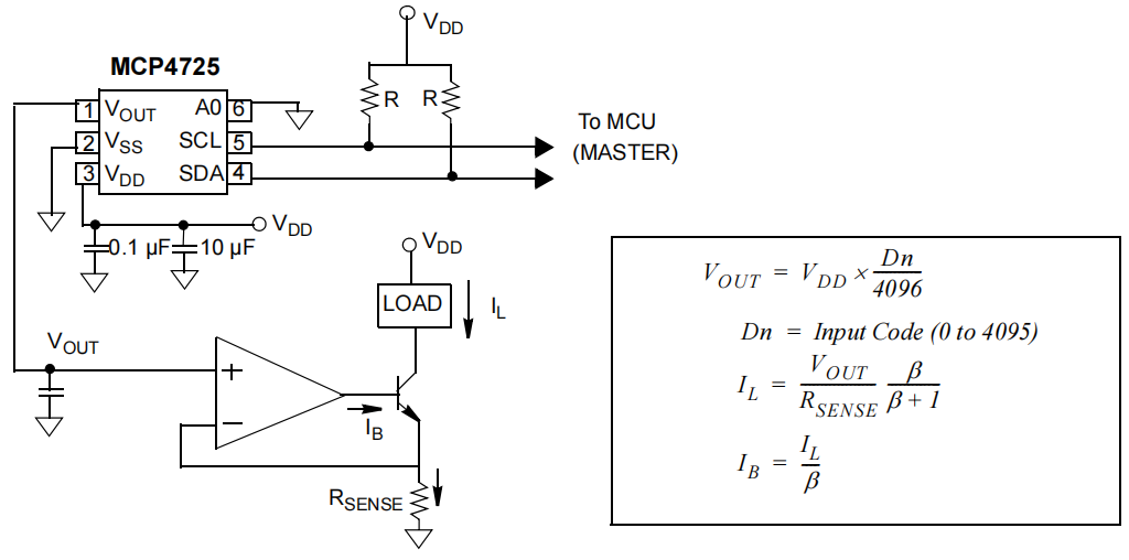
Op‑amp adjusts base current of the bipolar transistor. The sense‑resistor voltage‑drop forms feedback, forcing stable constant load‑current regardless of supply variations.