



MCP41010 Deep‑Dive: SPI Protocol & Hands‑on Implementation
MCP41010 principle SPI driver practical cases
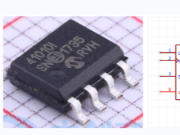
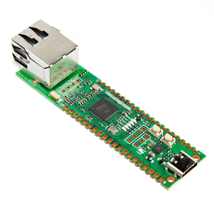
- Introduction to MCP41010 Digital Potentiometer
MCP41010 is a single‑channel, 8‑bit resolution digital potentiometer, available in 10 kΩ, 50 kΩ and 100 kΩ total‑resistance variants, controlled via SPI interface.
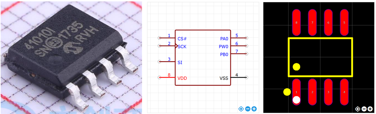
Main features:
256‑tap adjustment 256 adjustable tap positions for precise resistance setting.
High accuracy Maximum Integral Non‑Linearity and Differential Non‑Linearity of ±1 LSB, guaranteeing accurate resistance control.
Low power consumption Built on low‑power CMOS technology; maximum quiescent supply current is only 1 µA, suitable for low‑power applications.
Single‑supply operation Operating supply‑voltage range: 2.7 V to 5.5 V.
Software power‑down function On‑chip software power‑down feature can disconnect the entire resistor network to minimize power consumption.
Mid‑scale reset On power‑up, the wiper resets to the mid‑position (0x80), ensuring consistent initial state.
MCP41010 has eight pins, key pin descriptions:
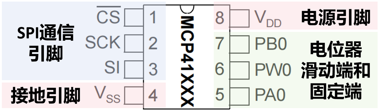
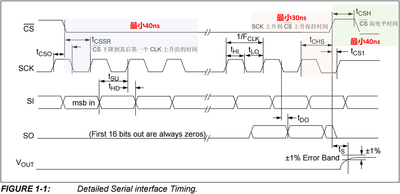
Chip‑select pin CS SPI chip‑select pin for device selection. SPI interface activates when CS goes low and starts receiving data. After data is loaded into the shift register, a high‑going transition on CS latches and executes the command.
Clock pin SCK SPI clock pin for synchronizing data transfer. Data is sampled on the rising edge of SCK via the SI serial‑data‑input pin.
Data‑input pin SI SPI serial‑data‑input pin for receiving commands and data bytes.
Power‑supply pin VDD Positive power‑supply input pin, operating voltage 2.7 V‑5.5 V.
Ground pin VSS Device ground pin connected to power‑supply negative rail.
Fixed terminals PA0 and PB0 Two ends of potentiometer‑0 resistor array. The wiper terminal PW0 slides between PA0 and PB0. The resistance between PA0 and PW can be adjusted from 0 Ω up to full‑scale resistance.
Wiper output terminal PW0 Wiper tap point of the resistor network. Control commands adjust resistance distribution between PA0 and PB0. Output voltage or resistance is available at this pin.
- MCP41010 Internal Structure and Operating Principle
MCP41010 internal blocks include power‑supply input, control logic, 16‑bit shift register, resistor array, tap‑control register and SPI interface pins.
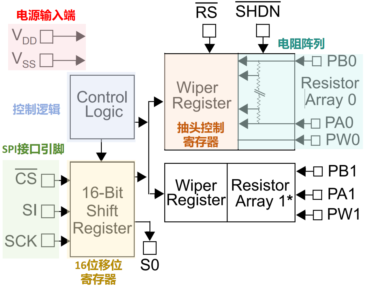
Function of each block:
Power‑supply input (VDD and VSS) Provides operating supply for single‑supply operation (2.7 V‑5.5 V). Supply voltage and current specifications are listed in the datasheet.

Control logic Decodes incoming SPI commands and data, updates the internal tap‑control register accordingly.
16‑bit shift register Receives external commands and data via SPI, shifting bits synchronized to SCK clock. After receiving a full 16‑bit word, control‑logic decodes the command and sets the wiper tap point of the resistor array.
Resistor array Fixed resistor ladder network with 256 equal‑value tap segments.
Tap‑control register Stores 8‑bit wiper‑position data (0x00 ~ 0xFF). The wiper divides the resistor array into two resistance segments between PA and PB, with PW as wiper output.
In short, resistance adjustment or voltage‑divider functionality of MCP41010 is realized by its resistor‑ladder network.
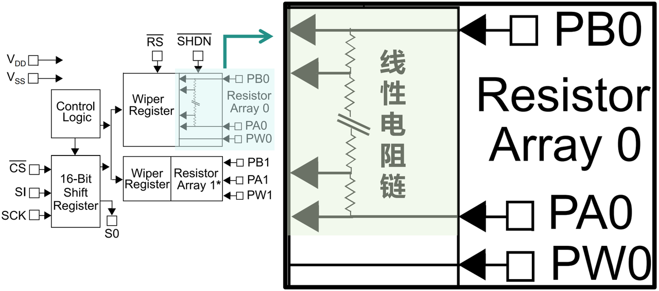
The resistor array consists of series‑connected fixed‑value resistor cells (for MCP41010 10 kΩ variant each unit is ~52 Ω), forming a linear resistor chain whose two ends connect to PA and PB pins. The MCU sends target resistance values over SPI. The on‑chip control‑logic updates the 8‑bit tap‑control register (0x00‑0xFF). Each digital value corresponds to one tap node on the ladder. The wiper PW can switch between these nodes, changing resistance between PA‑PW or PW‑PB.
- MCP41010 SPI Communication Protocol
MCP41010 requires a 16‑bit word sent from MCU over SPI for every operation. The first 8 bits form the command byte, the second 8 bits form the data byte. Transmission starts by pulling CS chip‑select low. All data bits are sampled on rising edges of SCK; SCK idles low. After finishing the 16‑bit transfer, CS is pulled high. MCP41010 writes the data byte into the tap‑control register and clears the 16‑bit shift register.
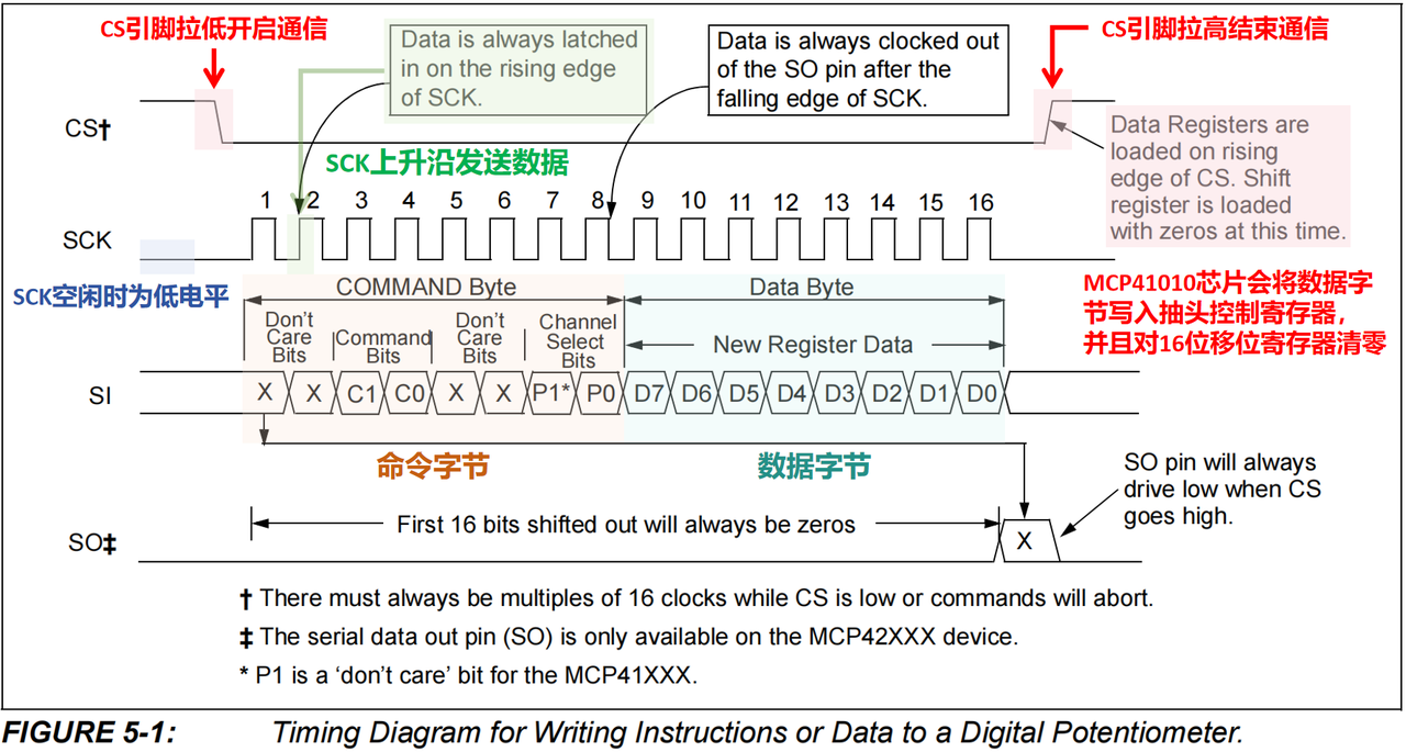
The command byte (first 8 bits) contains command‑select bits (C1, C0 at bit4‑bit5), potentiometer‑select bits (P1, P0 at bit0‑bit1), plus unused don’t‑care bits which have no effect on execution.
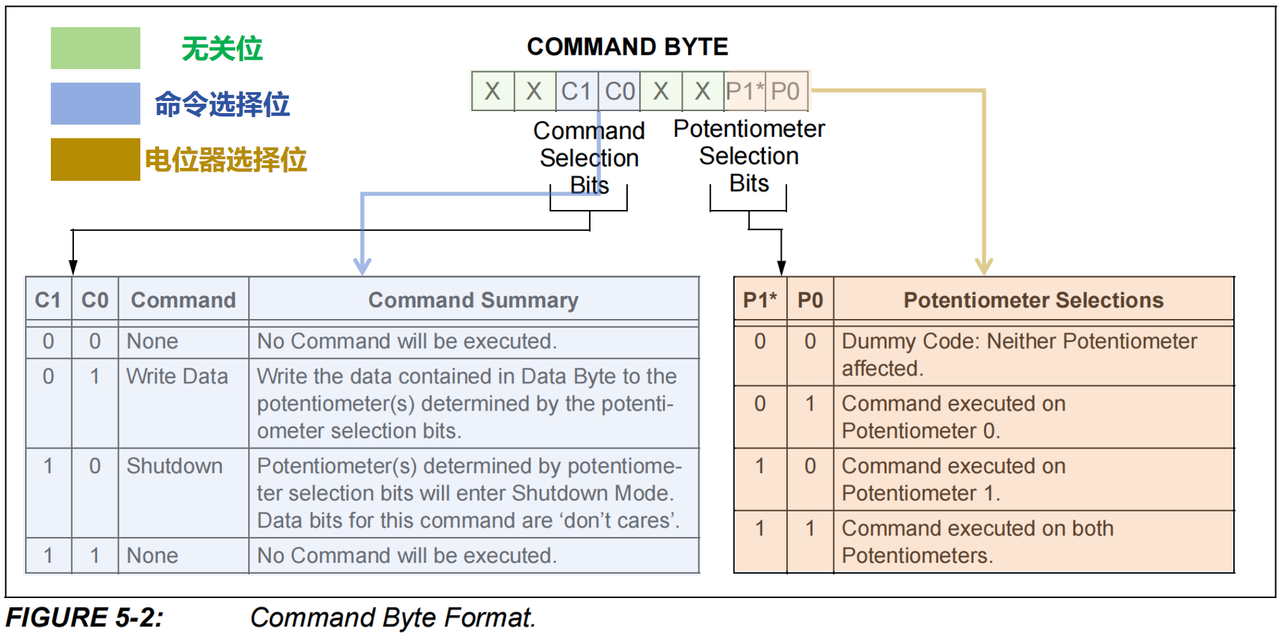
Meaning of command‑select bits C1, C0 (bit4‑bit5):
C1,C0 = 00 or 11: No operation executed. C1,C0 = 01: Write data byte into the selected potentiometer. C1,C0 = 10: Put selected potentiometer into power‑down mode; data byte bits are don’t‑care.
For MCP41010 single‑channel digital potentiometer, potentiometer‑select bits (P1, P0, bit0‑bit1) are always set to 01. The data byte (second 8 bits) sets new tap value, valid range 0‑255.
MCP41010 SPI electrical specifications:
Maximum SPI clock frequency is 10 MHz. Key timing parameters are marked below.
- MCP41010 Operating Modes and Application Examples
MCP41010 supports two operating modes.
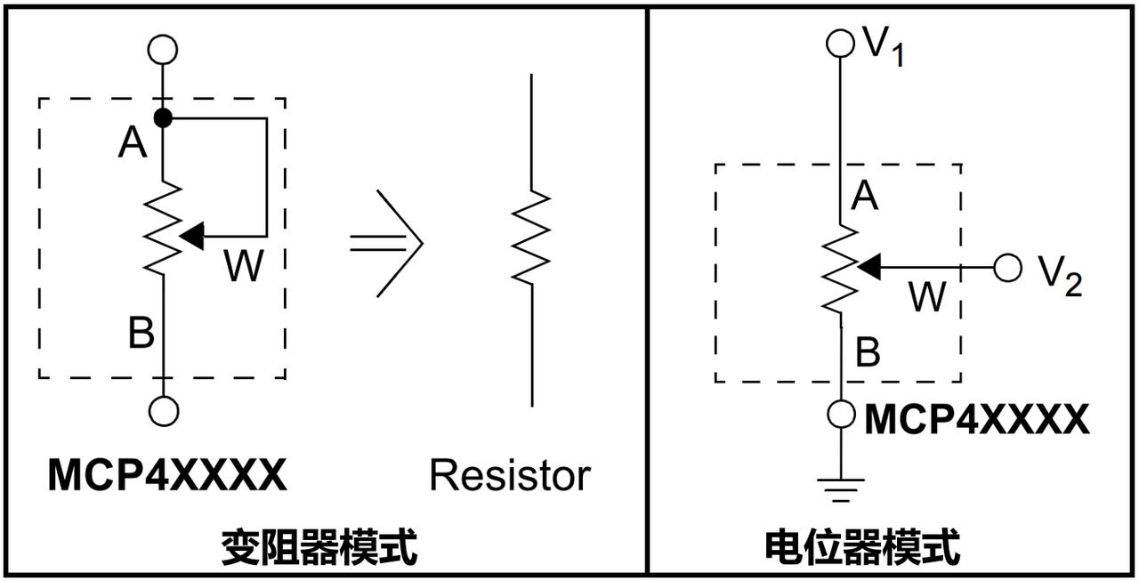
Rheostat mode In rheostat mode MCP41010 acts as a two‑terminal variable resistor. PA and PW terminals are shorted together, PB connects to the other circuit node. Adjusting tap position changes resistance between PA/PW and PB. Minimum value is 0x00 (~52 Ω), maximum value is 0xFF (near full‑scale resistance). Each LSB step equals total‑resistance / 256. Important note: wiper current must stay within 1 mA to avoid damaging internal circuitry.
Potentiometer mode All three terminals PA, PB, PW are connected to the circuit forming a voltage divider. PA and PB connect to power or signal input; PW outputs divided voltage. Adjusting tap position changes output voltage at PW. $$ V_W = V_A \times \frac{R_{AW}}{R_{AB}} + V_B \times \frac{R_{WB}}{R_{AB}} $$ Where $V_A$ and $V_B$ are input voltages at PA and PB; $R_{AW}$ and $R_{WB}$ are resistances on each side of wiper; $R_{AB}$ is total resistance between PA and PB.
Example of gain‑adjustable amplifier circuit using MCP41010 digital potentiometer and MCP606 op‑amp:
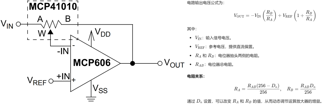
MCP606 is configured as inverting amplifier. Setting wiper‑tap position of MCP41010 changes divider ratio and thus amplifier gain.
MCP41010 10 kΩ version uses ~52 Ω per tap step. For higher‑precision fine trimming, two MCP41010 devices can be cascaded: one for coarse adjustment, one for fine adjustment.
In this topology MCP1 (coarse‑adjustment) sets main resistance range, MCP2 (fine‑adjustment) performs small‑step trimming. MCP1‑PW connects to MCP2‑PA. MCP2‑PW serves as final output. Both MCP1‑PB and MCP2‑PB tie to GND, PA terminals receive input signal. They share the same SPI bus and use separate CS chip‑select pins for independent control. For example for 0‑10 kΩ total adjustment range: MCP1 handles coarse 0‑9 kΩ range, MCP2 handles fine 0‑1 kΩ trimming.
- MCP41010 Usage Notes
MCP41010 is a resistor‑ladder digital potentiometer. On‑chip stray capacitance and parasitic inductance limit usable signal bandwidth. According to datasheet and practical testing, signal gain degrades significantly above 1 MHz, causing amplitude roll‑off or waveform distortion.
If you need amplitude control for high‑frequency signals inside op‑amp circuits, use high‑bandwidth digital potentiometers such as AD5292 or MAX5481, or substitute with Programmable Gain Amplifier (PGA).
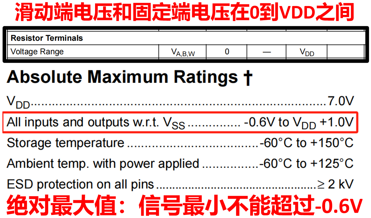
Also note MCP41010 is single‑supply device (typical 2.7 V‑5.5 V VDD). Its signal‑handling range is limited between 0 V and VDD. Negative‑voltage input signals (e.g. zero‑centered sine‑wave) will suffer signal distortion.