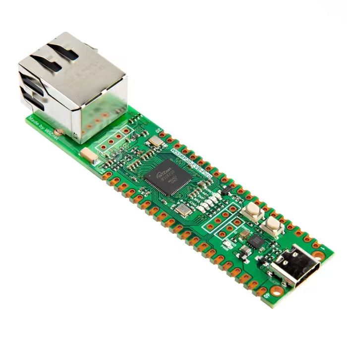
【Preliminary Note】The original hardware example in this article was written based on the RP2040. The actual hardware used in this hands-on demonstration features the W55RP20 as the main controller chip. The circuit logic and UF2 flashing operation principles are universally applicable, with only the main controller model differing. The original chip model mentioned in the circuit descriptions below is provided for reference purposes only.
Tweet:
Basic Structure and Concepts of Timers
The clock serves as the "fundamental beat" for all hardware (including timers) operation of the Raspberry Pi Pico: different peripherals require clocks of varying frequencies to function, and the clock system of the Pico operates in two steps:
Clock Source Acquisition: Acquire raw clock signals from multiple stable "basic clock sources"(e. g., crystal oscillators, oscillators);
Clock Distribution: The process of distributing the original clock signal to different peripherals (such as timers, UARTs, ADCs) after subjecting it to frequency division (frequency reduction) and enabling (on-off control).
Next, we will briefly introduce the basic structures and concepts of the general-purpose timer, PWM timer, and Systick system tick timer. In the Raspberry Pi Pico, in addition to the common general-purpose timer, PWM timer, Systick system tick timer, RTC real-time clock, and WDT watchdog timer, the following peripherals also have their own independent timers:
PIO finite-state machine: It is equipped with a 32-bit timer that can generate interrupts, and its operating frequency is equal to the system clock frequency (clk_sys, the core clock for the processor and bus, typically 125MHz);
DMA: It has four internal pacing timers that operate independently, and their clock is correlated with the clock of the DMA peripheral (typically clk_peri).
1. General-purpose timer
The universal timer of Raspberry Pi Pico has the following features:
64-bit standalone increment counter: with a fixed frequency of 1 MHz, the count increments by 1 every 1 microsecond;
4 alarm modules: An interrupt will be generated when the lower 32 bits of the 64-bit counter match the set value of the alarm.
The counter can be read from a pair of latch registers, so there is no need to consider race issues when multiple processors access it simultaneously.
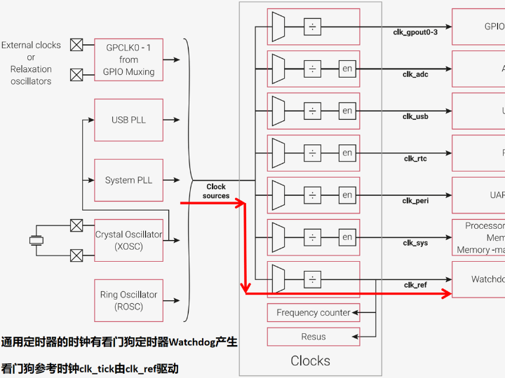
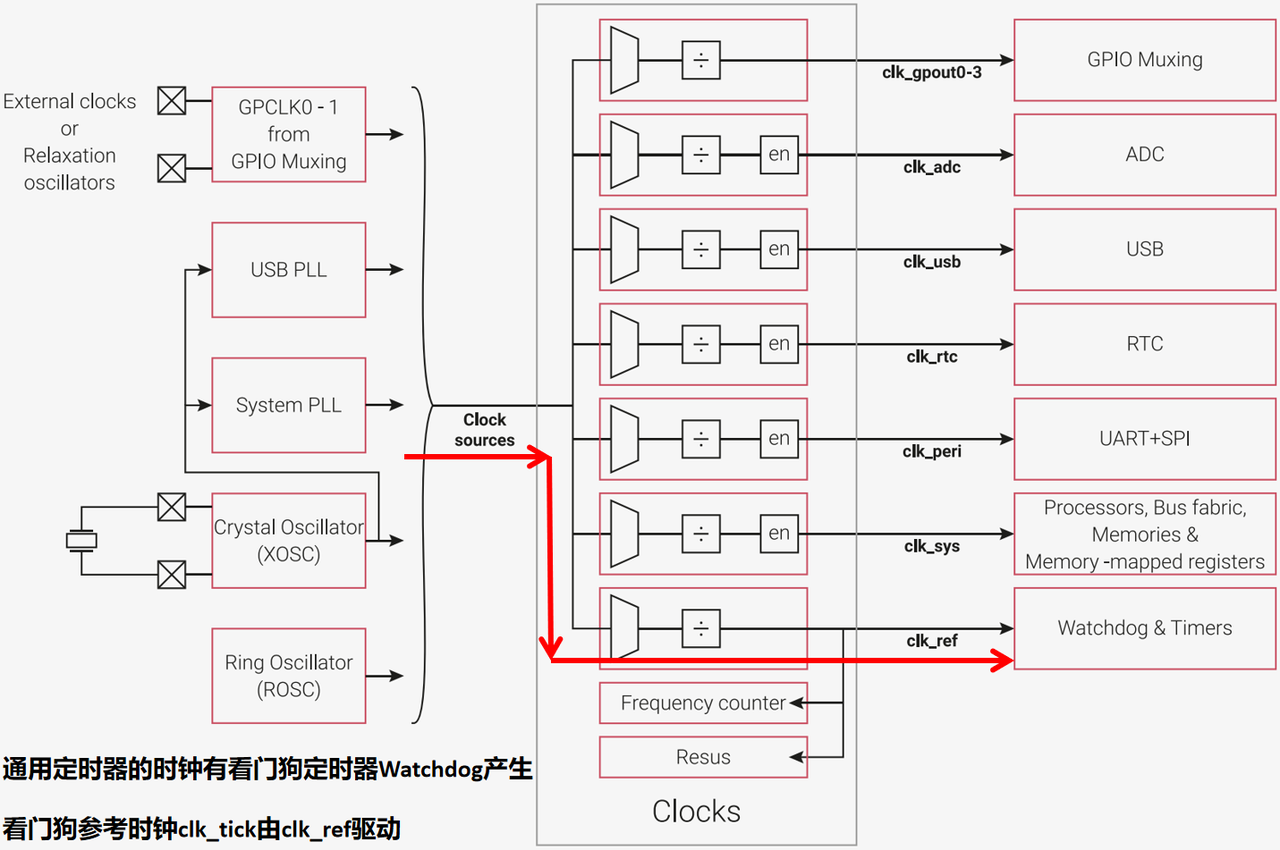
The clock input of the general-purpose timer is provided by the watchdog timer at a frequency of 1 MHz:
The red module on the left side of the diagram is the "original clock source" of Pico, which provides base clocks with different characteristics:
Crystal Oscillator (XOSC): An external crystal oscillator (typically 12 MHz), which serves as the most stable clock source;
Ring Oscillator (ROSC): An on-chip ring oscillator that features fast startup but relatively low accuracy.
USB PLL/System PLL: Phase-locked loop circuits that can multiply the base clock to a higher frequency (for example, the System PLL can output 125MHz as the system core clock);
GPCLK0-1: External clock input to reuse from GPIO pins;
External clocks/Relaxation oscillators: Other external clocks or relaxation oscillators.
The module on the right side of the diagram is the "Clock Distribution Unit": it selects a clock source from the "Clock sources" on the left, adjusts the frequency via the "frequency divider (marked as ÷ in the diagram)", controls on/off through the "enable switch (en)", and then sends the clock to the corresponding peripheral. The key association related to timers is as follows:
clk_ref clock: assigned to "Watchdog & Timers";
Clock of the general-purpose timer: It is obtained after the clk_ref is processed by the watchdog, with a frequency of 1MHz.
1.1 Counter Unit
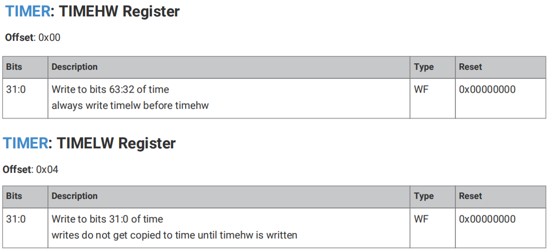
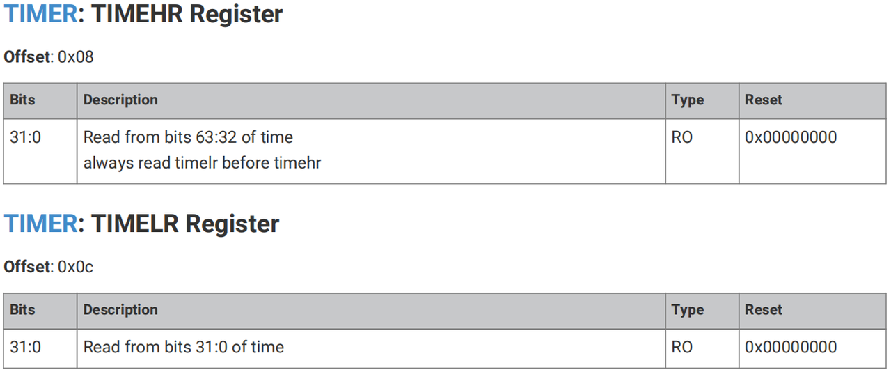
The timer features a 64-bit counter, while the RP2040 only has a 32-bit data bus. This means that reading and writing the TIME counter value each require operations via a pair of registers (the base address of the timer registers is TIMER_BASE 0x40054000):
Write the time via the TIMEHW register (for writing upper 32-bit data) and the TIMELW register (for writing lower 32-bit data):
Use the TIMEHR register (to read the upper 32 bits of data) and the TIMELR register (to read the lower 32 bits of data) to read the time:
It should be noted that although it is theoretically possible to enforce a new time value by writing to the TIMEHW and TIMELW registers, this practice is discouraged. This is because the timer value is expected to be incremented monotonically by the Pico SDK.
1.2 alarm Unit
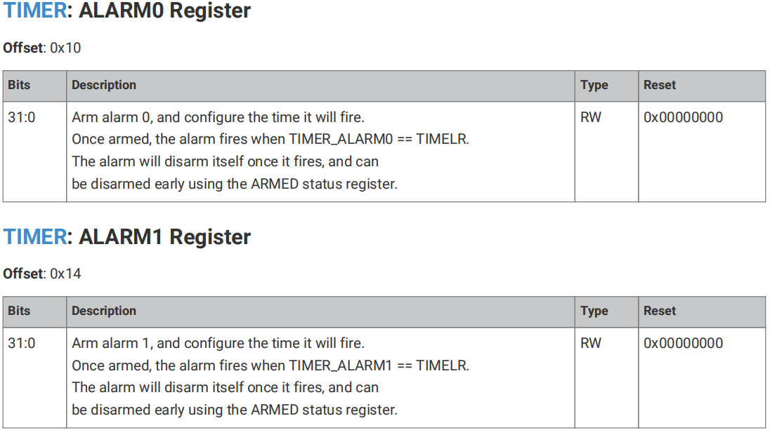
The timer has 4 alarm units, and each alarm unit can output an independent interrupt. Since the alarm units match the lower 32 bits of the 64-bit counter, the upper time limit for the alarm units to count is 2^32 us = 4295 s = 72 min.
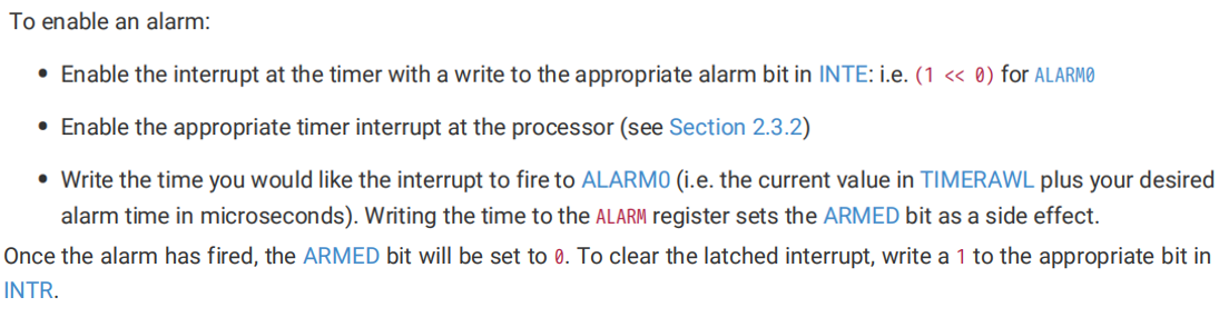
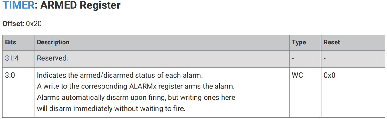
If the alarm unit needs to be enabled, the following registers shall be configured:
ALARMx (x = 0~3) Register: Used to set the alarm time; when the set time is reached, a fire event will be triggered and an alarm will be generated.
ARMED Register: Indicates whether each alarm generates an alert
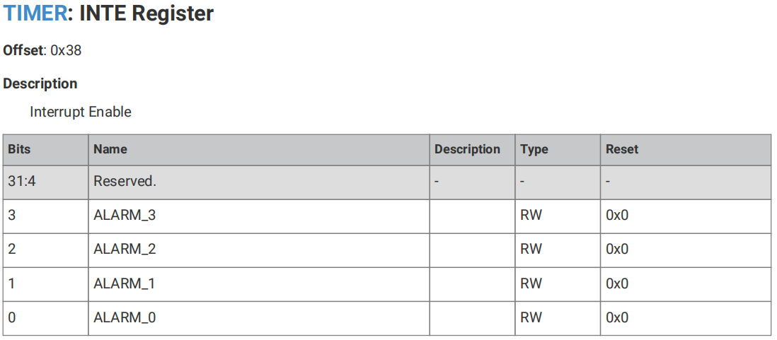
INTE register: enables or disables the alarm interrupt
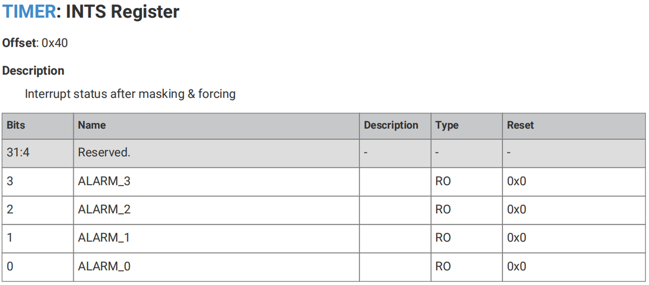
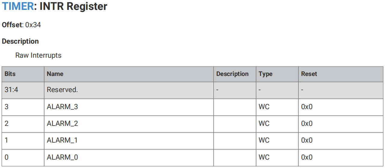
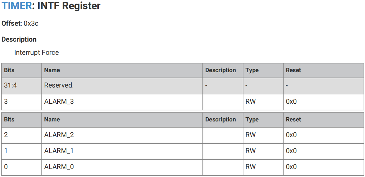
INTR register, INTF register, INTS register: Check the alarm interrupt status or force an interrupt to be generated
2. PWM Timer
2.1 Basic Structure and Characteristics of PWM Timer
The PWM timer incorporates 8 "nearly independent" 16-bit programmable counters, which share the same 125 MHz input clock (system clock) while featuring mutually independent clock dividers.
The PWM timer of Raspberry Pi Pico has the following features:
Each counter channel has two outputs (16 PWM channels in total), which can be connected to any of all GPIO pins.
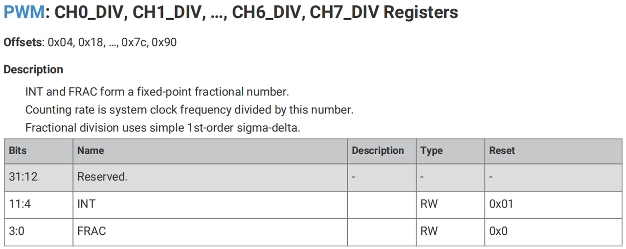
The frequency divider features 8-integer and 4-decimal frequency division, and the signal output frequency adjustable via 16-bit PWM ranges from 125 MHz to 7 Hz.
The adjustable duty cycle range for each PWM output channel is 0 to 100.
can generate interrupt requests or trigger DMA
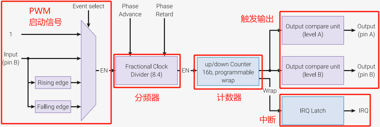
One of the two channels of each counter can be used as an input to serve as the start signal for PWM output; this input supports rising-edge triggering, falling-edge triggering, or high-level triggering, and this function can be applied to measure the frequency and duty cycle of external signals.
Phase is adjustable when the timer increments
All channels can be started synchronously and enabled to implement power control
The correspondence between each GPIO and PWM channel is as follows:
The same PWM output can be selected on two GPIO pins; the identical signal will appear on each GPIO.
2.2 Start Signal of PWM Channel
Here, the B pin of the PWM channel can be used as the start signal for PWM. It should be noted that when the B pins of multiple PWM channels are used simultaneously, the signals on these B pins are processed through an OR operation before serving as the PWM start signal.
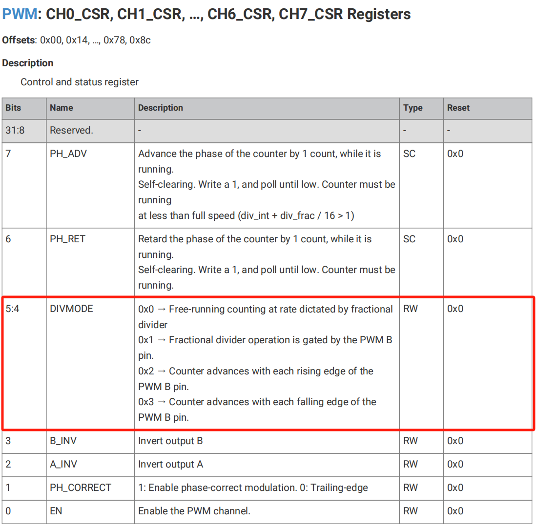
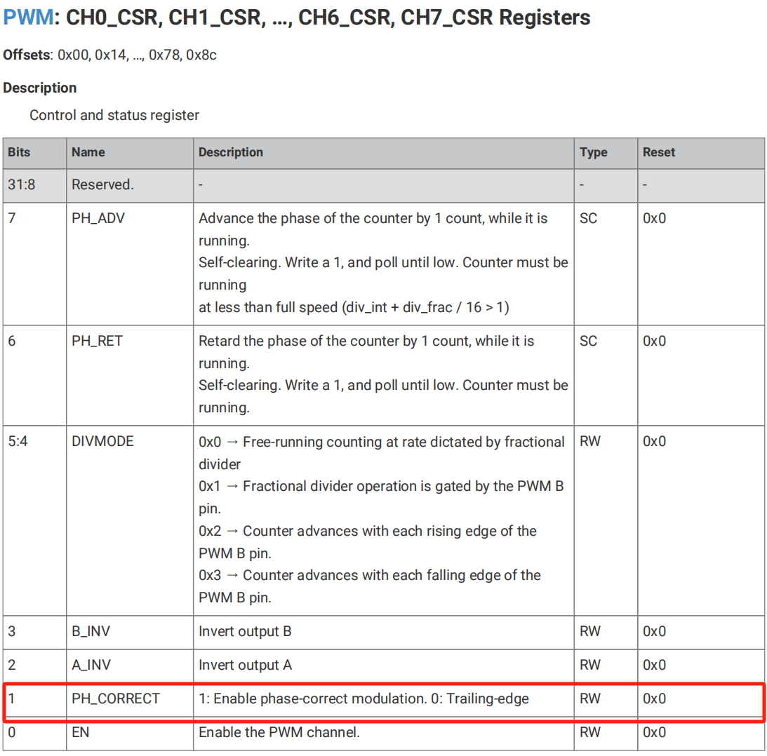
We can configure the DIVMODE bit in the CSR register to select rising-edge triggering, falling-edge triggering, or high-level triggering:
2.3 Working Principle and Counting Modes of PWM Timer
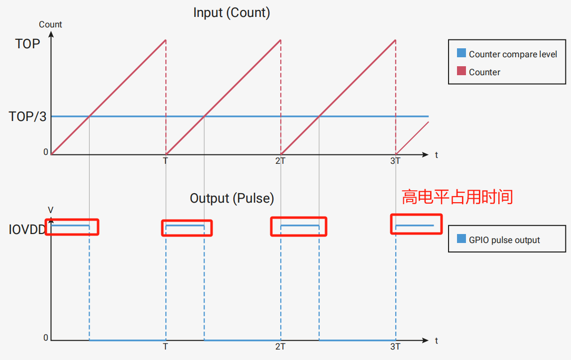
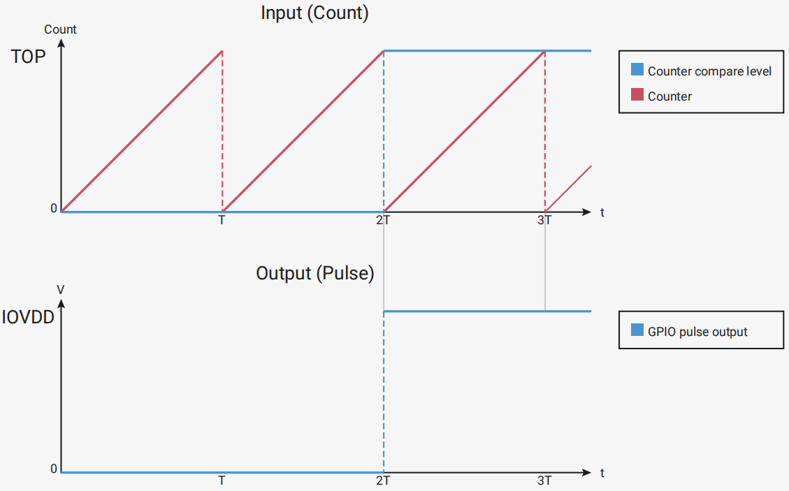
Simply put, the operating principle of a PWM timer is as follows: there is a timer inside the PWM, which increments along with the clock cycle, and with each increment, it compares the current count value of the counter with the preset count value:
When the count value of the current counter reaches the preset count value: The GPIO pin corresponding to the PWM channel outputs a high level
When the count value of the current counter > the preset count value: the GPIO pin corresponding to the PWM channel outputs a low level
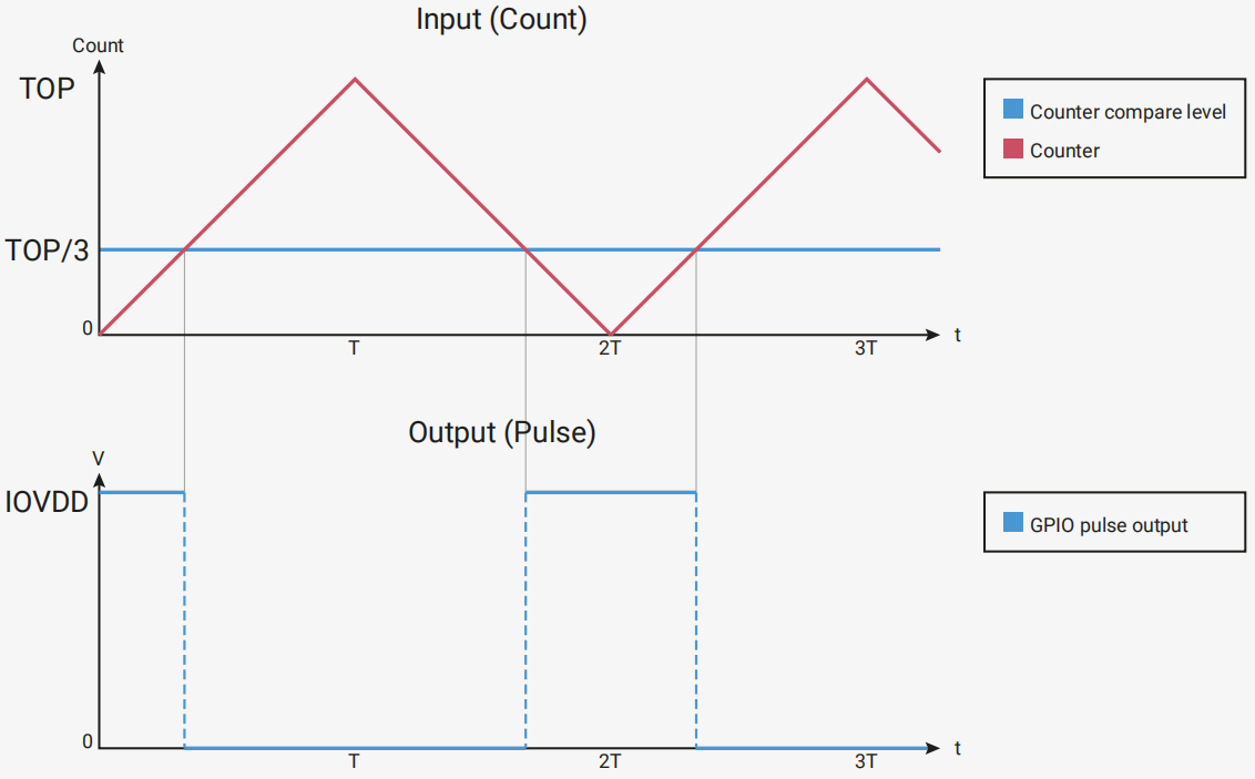
The figure above shows the up-counting mode of the PWM timer (the output is pulled low when the set value is reached), and the PWM timer also supports the center-aligned counting mode:
The two counting modes can be switched via the PH_CORRECT bit of the CSR register:
2.4 Modification of PWM Parameters
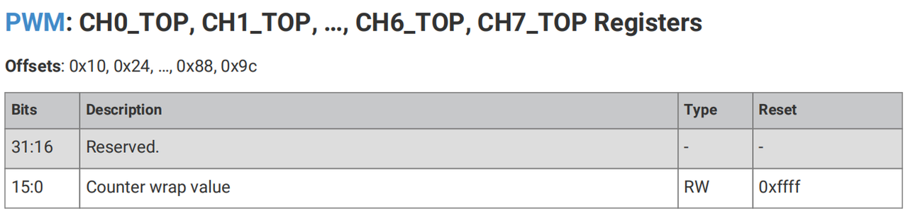
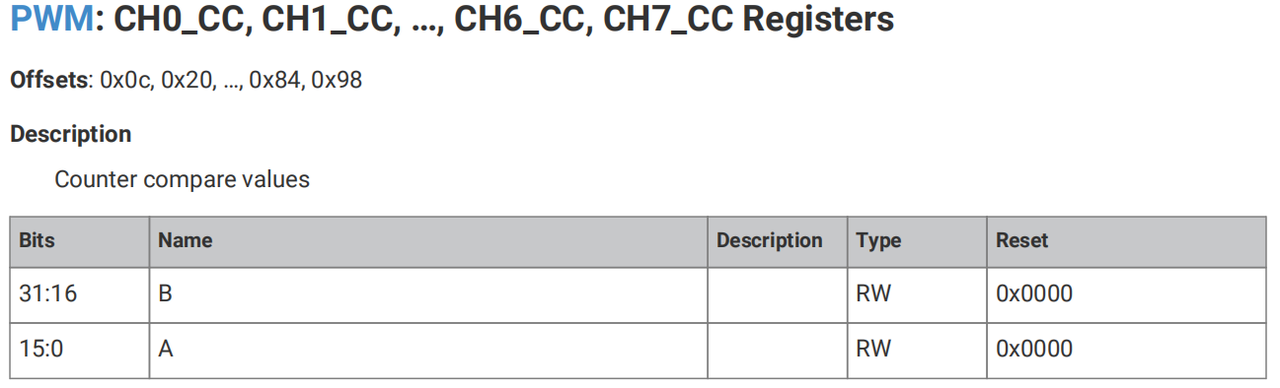
Here, the counting period (i. e., the maximum count value) of the PWM timer is controlled by the TOP register, with a maximum period of 65536 clock cycles; the counter comparison value is controlled by the CC register, and the clock division is controlled by the DIV register.
The PWM output period and frequency can be calculated using the following formula:
The output duty cycle of the PWM timer can vary between 0% and 100%. A CC value of 0 will produce a 0% output, while a CC value of TOP + 1 will produce a 100% output:
2.5 Dual Register Mechanism of PWM Timer
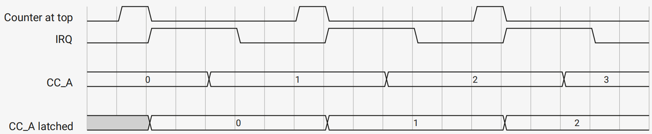
Here, it should be noted that the TOP register and CC register of the PWM timer feature a dual-register mechanism. Simply put, the TOP register and CC register actually consist of the following components: a preload TOP register, a shadow TOP register, a preload CC register, and a shadow CC register. The shadow register is the one that actually functions, while the preload register serves as a buffer for the shadow register to prepare data or instructions in advance.Since timers typically operate in a periodic manner, if every parameter modification we make is directly applied to the actual registers, it will inevitably interfere with the normal counting of the current cycle and the associated output operations.
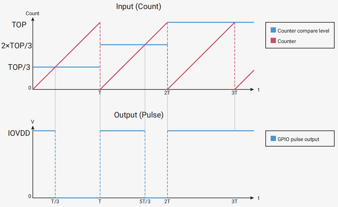
Consider this scenario: when we need to switch the duty cycle of PWM, we have to modify the value in the timer CC register. The ideal situation we expect is as shown in the figure below: when we modify the value in the timer CC register, there is a high probability that the current PWM timer is already in a counting cycle. We expect that the PWM wave output in the current cycle will follow the duty cycle set by the previous preset value, and only when the counter starts a new counting cycle will the output PWM wave generate a PWM wave with the corresponding duty cycle according to the newly set counting threshold this time:
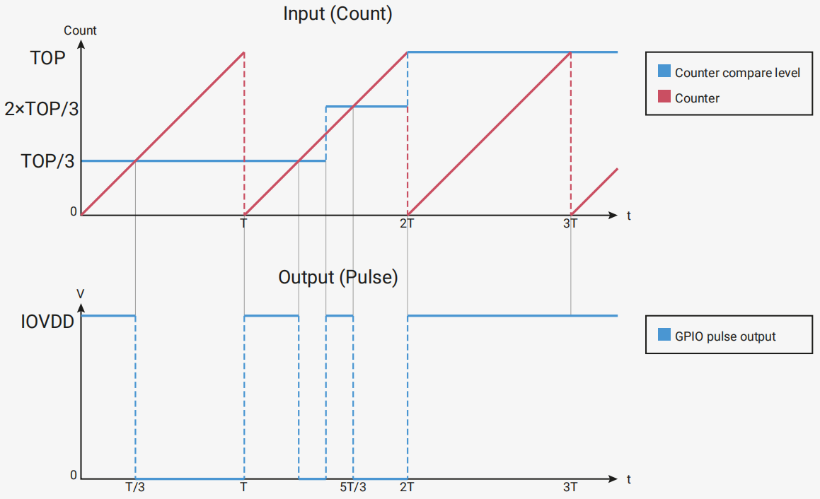
If the dual-register mechanism is not adopted, the count value preset by the user via software will be immediately updated to the CC register of the timer, which will cause abnormalities in the PWM waveform output:
Here, it should be noted that what users always operate via software is only the preload register. After we modify the value in the preload register, the shadow register will not immediately copy the value from the preload register; instead, it will transfer the value from the preload register to the shadow register only when the next update event occurs:
When the timer operates in up-counting mode: When the counter reaches the preset count threshold, the count value is cleared to generate an update event
When the timer is configured in center-aligned mode: An update event is generated when the counter stops counting down and starts counting up again
3. Systick System Tick Timer
3.1 Introduction to the Systick Timer
The SysTick timer, also known as the system tick timer, is a timer embedded in the Cortex-M0 core. All MCUs based on ARM Cortex-M series cores are equipped with this timer. Implementing delay functions or the heartbeat clock of an RTOS by using the core's SysTick timer will not occupy the system timer, thus saving system resources. Since SysTick is implemented inside the CPU core and is independent of MCU peripherals, its code can be ported between chips from different manufacturers.
The Systick timer in the Raspberry Pi Pico has the following features:
The frequency is 1MHz, with counting performed once every 1 microsecond
3.2 Controlling the Systick Timer
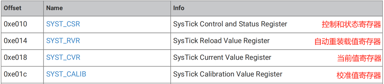
The Systick timer is mainly controlled by the following four registers (the base address of the Cortex-M0 core is PPB_BASE 0xe0000000):
Simply put, the operating principle of the SysTick timer is to count down continuously; when the current count value reaches 0, it automatically loads the initial timing value from the auto-reload register, and then proceeds with the next counting cycle.
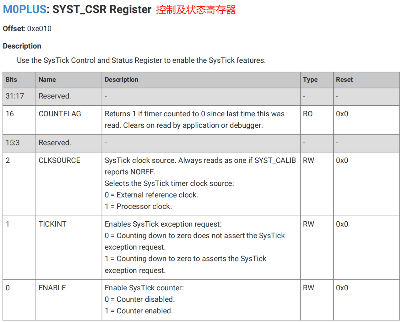
For the SYST_CSR register, there are the following four bits:
COUNTFLAG bit: Its main function is to prevent misreading and over-reading. If SysTick has counted down to 0 since the last time this bit was read, the value read this time will be 1; conversely, if this bit has not been read since the last operation, it will be automatically cleared after being read.
CLKSOURCE bit: It is mainly used to select the clock source, which can be either an external clock or the system clock.
TICKINT bit: Its main function is to select whether to generate an interrupt after the countdown ends.
ENABLE bit: disables or enables the Systick timer
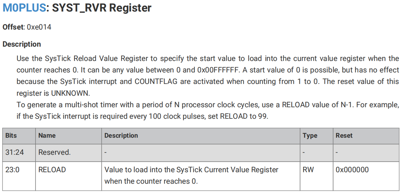
Use the SysTick SYST_RVR register to specify the start value to be loaded into the current value register when the counter reaches 0. It can be any value between 0 and 0x00FFFFFF, and when counting from 1 to 0, the SysTick exception request and count flag will be activated.
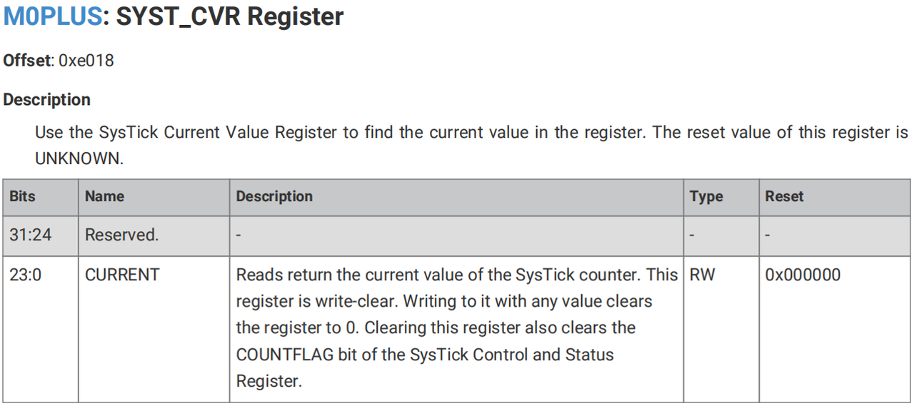
SYST_CVR can be used to obtain the current count value, and writing any value to it will clear the register to 0. Clearing this register will also clear the COUNTFLAG bit of the SysTick Control and Status Register:
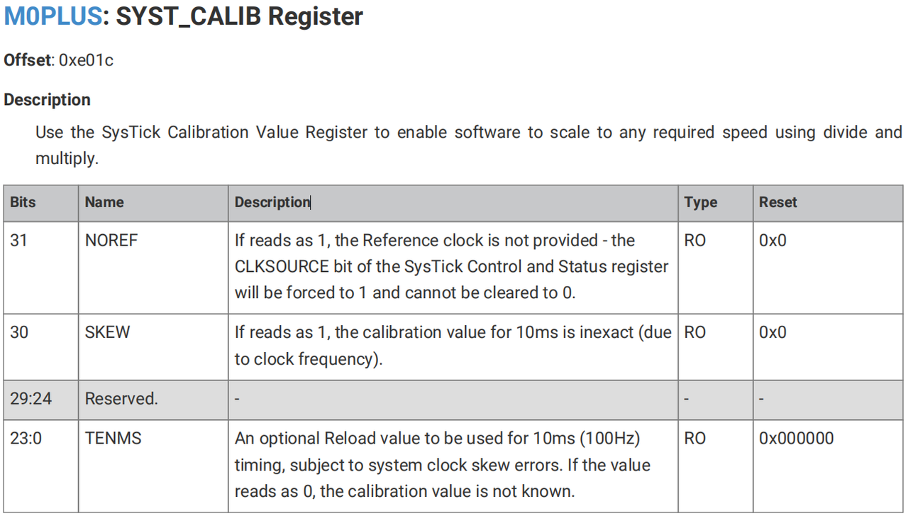
Calibrate or obtain the calibration status using the SysTick calibration value register: