



In‑Depth DAC Explanation: Operating Principles, Performance Parameters, Circuit Types and Practical
DAC conversion full explanation

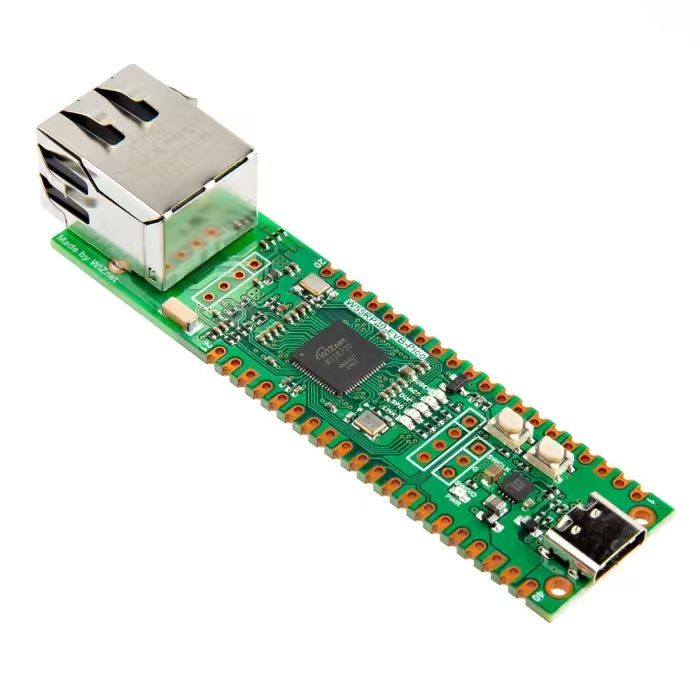
Digital‑to‑Analog Converter (DAC) is an electronic device that converts digital signals into analog signals. DACs are widely used in audio equipment, signal processing, communication systems, measuring instruments and other fields to restore processed digital data back into analog waveforms.

Digital‑audio processing example to explain DAC operation
In digital‑audio systems, the DAC plays a critical role. It converts digital signals stored inside audio files such as CD, MP3 and WAV into analog audio waveforms that can be played through speakers or headphones.
- Recording and digitization Recording devices use ADC (Analog‑to‑Digital Converter) to turn analog sound into digital form. These digital samples are saved as digital‑audio files like WAV or MP3.
- Digital‑signal transmission and processing When you play an audio file on a device, stored digital samples are read and processed by the processor. Processed digital data is then sent to the DAC for analog reconstruction.
- Digital‑to‑analog conversion and amplification The DAC receives processed digital values and gradually generates corresponding analog‑voltage waveforms approximating the original analog audio signal. The reconstructed analog signal is fed into an amplifier to boost signal strength.
- DAC Operating Principle and Basic Architecture
DAC inputs are binary digital signals made up of 0 and 1, obtained by sampling and quantizing continuous‑time, continuous‑amplitude analog waveforms. Three key functional building‑blocks are described below.

Core functional blocks of a DAC
Digital Processing Unit Digital signals are fed into the DAC in binary representation; each bit carries a specific signal weight. This unit receives input data from digital systems and contains input registers, decoding logic and control logic.
D/A Conversion Interface This is the core block of the DAC. It translates processed digital values into corresponding analog outputs using resistor networks, current‑steering arrays or other conversion techniques. Fundamentally, internal DAC circuitry maps each binary bit weight to an analog voltage or current. Weighted currents or voltages from individual bits are summed together to produce the final analog output corresponding to the digital input code.
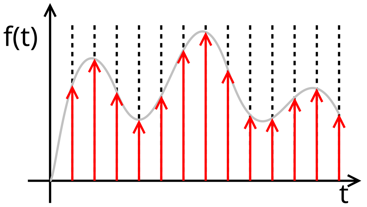
Reconstruction Filter Raw DAC output is normally a stepped waveform, where each sample produces a fixed‑level voltage or current. The reconstruction filter smooths these stair‑step outputs into continuous analog waveforms, removes high‑frequency artifacts generated during conversion, and suppresses aliasing effects.
Additional commonly‑included DAC components:
Output Amplifier Raw DAC analog outputs are usually weak and cannot directly drive loads such as loudspeakers or displays. The output amplifier boosts analog signals to appropriate amplitude for target loads. It also performs impedance matching to ensure reliable signal transfer and reduce reflection and distortion.
Reference Voltage DAC conversion accuracy depends heavily on its internal reference‑voltage source. It supplies a stable voltage benchmark for internal circuitry, guarantees conversion consistency, and defines maximum and minimum output levels.
Clock Generation Circuit Provides clock signals for DAC internal digital logic and sample‑timing control. These clocks set operating speed and data‑processing rhythm for the whole DAC.
- DAC Performance Parameters
DAC performance is defined by the following key specifications:
Resolution DAC resolution is specified in bits, representing how many distinct discrete voltage or current levels can be generated. Higher‑bit resolution yields finer signal representation. Resolution = 2^N, where N is DAC bit count. For example an 8‑bit DAC gives 2^8 = 256 output levels.
Sampling Rate Defines how fast the DAC updates analog outputs, measured in SPS (Samples Per Second). Higher sampling rates support higher‑frequency input signals and suit high‑speed signal‑processing applications.
LSB (Least Significant Bit) LSB corresponds to the analog‑signal increment represented by one least‑significant‑bit digital change. LSB value = (Maximum output voltage − Minimum output voltage) / 2^N. It determines DAC fundamental precision.
Linearity Deviation between actual DAC analog output and ideal theoretical value. Main metrics include INL (Integral Non‑Linearity) and DNL (Differential Non‑Linearity).
Dynamic Range Ratio between maximum‑amplitude output and minimum‑amplitude output, expressed in decibels (dB). Larger dynamic range means wider representable signal swing.
SNR (Signal‑to‑Noise Ratio) Ratio of desired signal amplitude versus noise amplitude at DAC output, measured in dB. Higher SNR indicates cleaner output quality.
Distortion Deviation of reconstructed analog waveform from the original ideal signal, mostly introduced by non‑linear behaviour. Main types are THD (Total Harmonic Distortion) and IMD (Intermodulation Distortion).
- DAC Types
3.1 Overview of DAC Architectures
Multiple DAC hardware architectures exist depending on implementation approach. Common D/A conversion structures:
Weighted‑Resistor DAC This DAC type uses resistor networks for digital‑to‑analog conversion. Each resistor corresponds to one binary bit. Higher‑weight bits use smaller resistance values. Digital codes switch individual resistors on or off. Total combined current generates analog output current, which is converted to output voltage via amplifier. The architecture is conceptually simple but requires highly‑accurate resistors.
R‑2R Ladder DAC Uses only two distinct resistance values R and 2R arranged in a ladder network to convert digital inputs into analog‑voltage outputs. It relaxes resistor‑precision matching requirements and lowers manufacturing demands.
Current‑Steering DAC Digital inputs toggle an array of current‑source switches. Total load current is adjusted to produce analog output. This architecture is well‑suited for high‑speed, high‑precision conversion.
Integrating DAC Employs integrating circuits such as capacitors and operational amplifiers to gradually build analog outputs matching input digital codes. Typically used for high‑precision but relatively low‑conversion‑speed applications.
3.2 Operating Principle of Weighted‑Resistor DAC
Block diagram of weighted‑resistor DAC conversion interface:
Basic weighted‑resistor DAC structure
Three fundamental building‑blocks:
Reference Voltage Provides stable reference level which defines the amplitude range for analog output.
Switches Switches controlled by digital‑code logic. They connect or disconnect individual resistors according to binary input bit value (0 or 1).
Resistors Resistor values follow geometric‑series weighting so each resistor contributes current with a 1/2 ratio relative to the next‑higher bit. Contribution of each resistor current diminishes progressively down the bit positions.
Take an 8‑bit weighted‑resistor DAC as example. Input digital code N = 11111111 = a8 a7 … a2 a1.
All switches are closed. Output voltage Vs is given by Vs = R2 * Ia. Total current: $$ I_a = \frac{E_{ref}}{R_1} \left( 1 + \frac{1}{2} + \frac{1}{4} + \frac{1}{8} + \frac{1}{16} + \frac{1}{32} + \frac{1}{64} + \frac{1}{128} \right) $$
Final output voltage Vs: $$ v_S = E_{ref} \cdot \left( \frac{1}{2^1} + \frac{1}{2^2} + \frac{1}{2^3} + \frac{1}{2^4} + \frac{1}{2^5} + \frac{1}{2^6} + \frac{1}{2^7} + \frac{1}{2^8} \right) $$
Now consider input digital code N = 01100100, with DAC reference voltage Eref = 10 V. Only switches K2, K3 and K6 are closed; all other switches remain open.
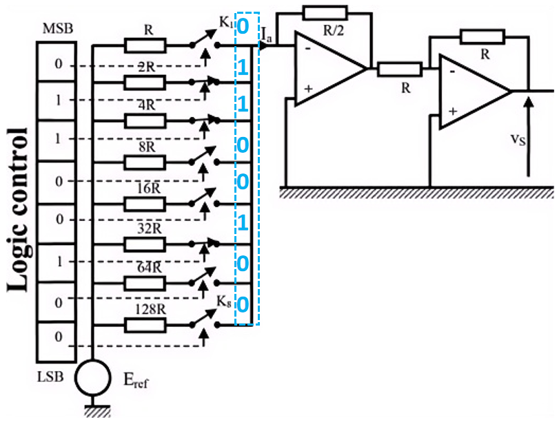
Switch status for input code N = 01100100 in weighted‑resistor DAC
Corresponding analog‑output‑voltage calculation: $$ v_S = E_{ref} \left( \frac{0}{2^1} + \frac{1}{2^2} + \frac{1}{2^3} + \frac{0}{2^4} + \frac{0}{2^5} + \frac{0}{2^6} + \frac{1}{2^7} + \frac{0}{2^8} \right) $$
The computed analog output voltage Vs equals 3.9 V.