



In‑depth Analysis of the 1‑Wire Protocol: Master Core Logic in One Article, from Physical Layer to R
This article details 1-Wire physical layer wiring, open-drain circuit, two power supply modes, standard communication flow, signal timings, ROM commands and uni
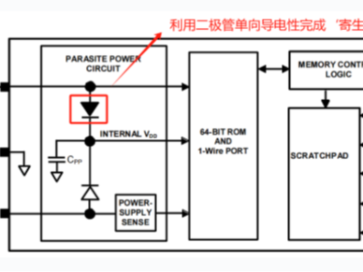
1.1 1-Wire Bus Connection Method
The 1-Wire bus uses only one wire to transmit signals and provide power. Communication is asynchronous and half-duplex, and follows a strict master/slave scheme. One or more slave devices can be connected to the bus at the same time. Only one master device can be connected to the bus.
1.2 Voltage Levels and Open-Drain Output
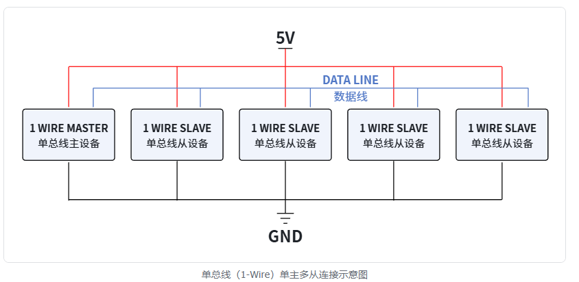
The 1-Wire protocol uses CMOS/TTL voltage levels. The maximum low level is 0.8V, the minimum high level is 2.2V, and communication is performed within a supply voltage range of 2.8V to 6V. The 1-Wire master or slave device is connected to the data line through an open-drain or tri-state port. The bus is at high level when idle; the high level is generated by a pull-up resistor, which is generally 4.7KΩ.
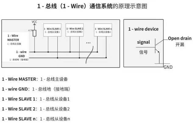
To ensure that some devices on the bus have sufficient current supply while working (for example, when the DS18S20-PAR temperature sensor performs temperature conversion, or when data is written to an E2PROM), in addition to the pull-up resistor, a MOSFET needs to be used on the bus to provide a strong pull-up supply. In most applications, this strong pull-up is not needed.
1.3 Powering 1-Wire Devices
1.3.1 Independent Power Supply
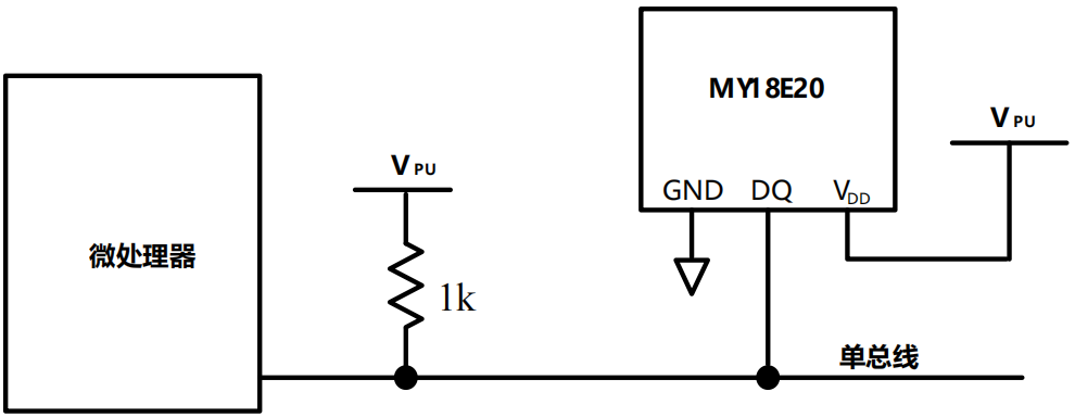
Taking the MY18E20 sensor as an example (i.e., a domestic replacement version of the DS18B20 sensor), we can supply power through the VDD pin from an external power source. The advantage of this mode is that no MOSFET pull-up is needed, and the 1-Wire bus can perform other operations arbitrarily during the temperature conversion process.
1.3.2 Parasitic Power Supply
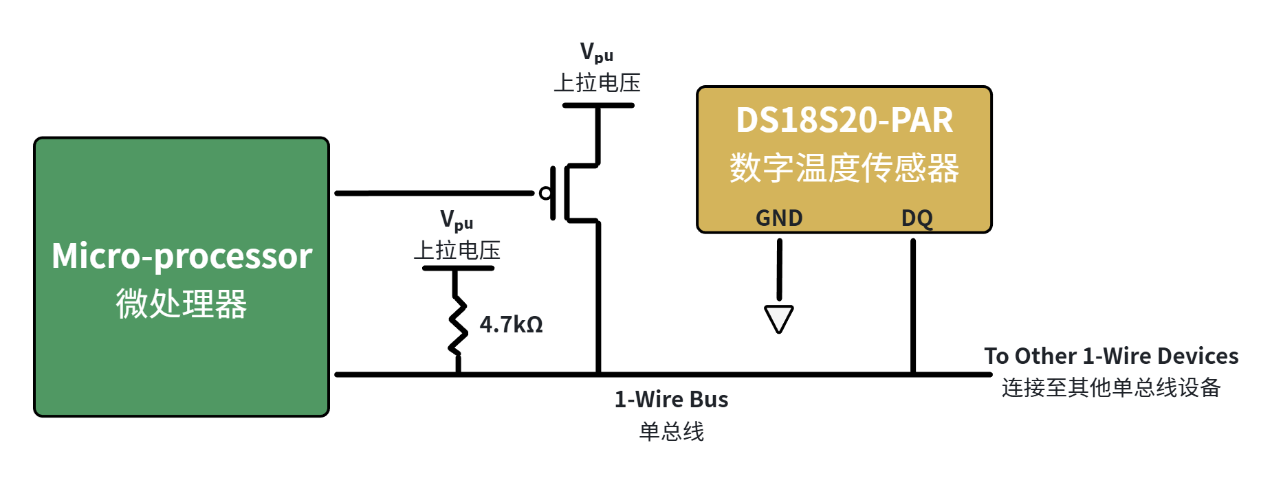
Taking the DS18B20 sensor as an example, we can use the MOSFET pull-up connection method to power the 1-Wire device:
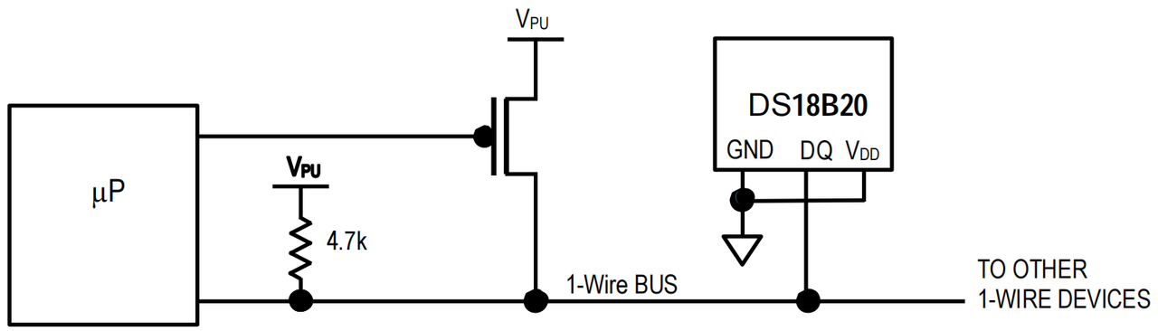
Parasitic power supply is mainly implemented using the unidirectional conductivity of a diode:
When the 1-Wire bus is at high level: through the diode and the pull-up resistor, Vpu supplies power to the chip and charges the capacitor Cpp
When the 1-Wire bus is at low level: the diode is cut off, and the capacitor Cpp supplies power to the chip
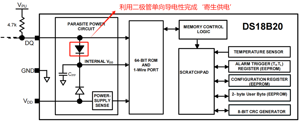
Here, parasitic power supply requires the 1-Wire bus to intermittently provide high level. On one hand, it charges the capacitor Cpp; on the other hand, when the bus remains low for more than 480us, the 1-Wire device will be reset.
2. Protocol Layer
2.1 1-Wire Communication Process
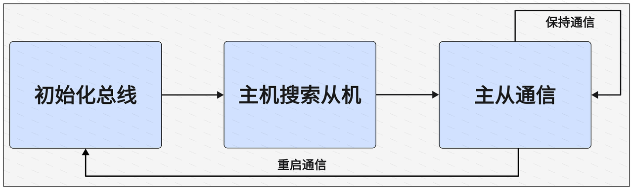
In 1-Wire communication, communication between the master and the slave can be completed in 3 steps:
Initialize the 1-Wire bus: the master sends a reset signal to reset the bus and synchronize the entire bus
Master searches for slaves: the master sends a ROM command to call the slaves; after a slave responds, the master selects a specific slave, and the other devices will exit and ignore the data subsequently sent by the master until the master sends the next reset signal and waits for the call again
Master and slave communicate: the master can send function commands to the slave or read/write data
2.2 1-Wire Communication Signals
The 1-Wire protocol defines the following communication signals:
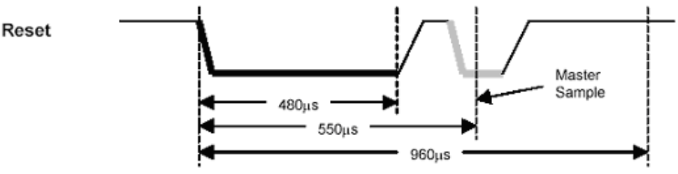
Master reset signal and slave presence signal: the master generates a reset signal by pulling the 1-Wire bus low for 480 ~ 960 us, then releases the bus and enters receive mode. When the master releases the bus, a rising edge is generated as the low level transitions to high level. After detecting the rising edge, the 1-Wire slave waits 15 ~ 60 us, then pulls the bus low for 60 ~ 240 us to generate the presence signal. If the master receives the slave's presence signal, it means the 1-Wire device is ready and the initialization process is complete.
Write data 0 signal: after the data line is pulled low, sample the data line within the 15 ~ 60 us time window. If the data line is low, it is a write 0; if the data line is high, it is a write 1. To generate a write data 0 signal, the master must pull the data line low and keep it low for 60us.

Write data 1 signal: after the data line is pulled low, sample the data line within the 15 ~ 60 us time window. If the data line is low, it is a write 0; if the data line is high, it is a write 1. To generate a write data 1 signal, the master needs to pull the data line low and then pull it high within 15us after the write data 1 signal starts.

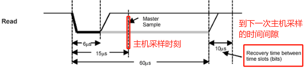
Read data signal: when the master pulls the data bus low, it should keep it low for at least 1us and then release the bus; it must read the data within 15us. Before the next master read signal, the bus should be pulled high for at least 1us.
2.3 ROM Commands
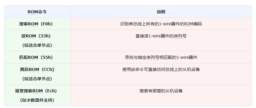
Note that the master must strictly follow the 1-Wire command sequence when accessing a 1-wire device, i.e., initialization, ROM command, function command. If the sequence is disordered, the 1-wire device will not respond to the master (except for the Search ROM command and the Alarm Search command). The 1-Wire protocol defines ROM commands, while function commands are determined according to the functions supported by the specific 1-wire device.
Common ROM commands are as follows:
2.4 Addressing Method
Each 1-Wire slave stores a unique 64-bit serial number in its ROM, which is used as its node address. The master identifies the slaves connected to the bus network through the ROM ID. The ROM ID cannot be changed and is laser-engraved inside the 1-Wire device.
The ROM ID consists of eight bytes and is divided into three main parts: starting from the LSB, the first byte stores the 8-bit family code that identifies the device type.
The next 6 bytes store a customizable 48-bit individual address. The last byte is a CRC check code calculated from the first 56 bits of the ROM code.