Getting Started with Embedded Low-Level Systems: The Actual Purposes of ROM, SRAM and Flash in the R
This article defines address mapping, register mapping and remapping, which establish address indexing rules for all internal chip resources.
COMPONENTS
PROJECT DESCRIPTION
Memory
Here, we will first clarify several core concepts of "mapping"(which serves as the foundation for memory access), before explaining the address mapping tables for memory and SRAM. For the resources inside a chip (including memory, registers, and peripherals) to be accessible, they must first be assigned "house numbers" — and this is precisely the essence of "mapping":
Address mapping: The process of assigning a unique "digital house number"(i. e., system address) to all resources in a chip. For example, the address range of SRAM starts at 0x20000000, and that of ROM starts at 0x00000000. The core and DMA can accurately locate the resources to be accessed via these "house numbers", which essentially functions as a mapping table between resources and their corresponding addresses.
Register mapping: It is a subset of address mapping, which assigns addresses to the registers (small memory units for storing configurations and statuses) inside a chip. For example, "0x40008000 corresponds to the baud rate register of the UART" — when software writes to this address, it can configure the UART, which is equivalent to a "correspondence table between register functions and their addresses";
Remapping: refers to "reassigning house numbers" — for example, if house number A originally corresponds to memory, after remapping, house number A can correspond to a peripheral device, which flexibly adjusts the access address of resources to adapt to different scenarios.
Memory access is entirely based on address mapping. Let's take a specific look at the memory of the RP2040: the RP2040 has built-in ROM and SRAM, and accesses external Flash via the QSPI interface.
1.ROM
16kB Read-Only Memory (ROM) at address 0x00000000. The content in the ROM is fixed once the chip is manufactured, acting as a "pre-installed toolkit that comes with the chip", which contains:
Initialize the boot routine
Flash boot sequence
Flash Programming Routine
USB mass storage device supporting UF2
Utility libraries, such as fast floating-point
The ROM bootloader can be downloaded at the following link: https://github.com/raspberrypi/pico-bootrom
This ROM supports single-cycle read-only bus access and is connected to a dedicated AHB-Lite arbiter, so it can be accessed concurrently with other memory devices. Attempts to write to the ROM have no effect, and no bus fault will be generated.
2.SRAM
The on-chip SRAM totals 264 kB, which is physically divided into six banks, a design that significantly boosts the memory bandwidth for multiple masters (i. e., it allows multiple bus masters such as Core0, Core1, and DMA to "access different banks simultaneously" to avoid resource contention), while software can treat it as a single 264 kB memory region for read and write operations (access to the physical banks is implemented via address mapping).
There are no restrictions on the content stored in each bank: it can hold applications, data buffers, etc.
A bank can be divided into four 16k x 32-bit blocks (each of 64 kB) and two 1k x 32-bit blocks (each of 4 kB).
Each SRAM bank can be accessed via a dedicated AHB-Lite arbiter, which means different bus masters can access different SRAM banks in parallel, allowing up to four 32-bit SRAM accesses (one per master) per system clock cycle.
In memory mapping, the start address of SRAM is 0x20000000, and the base address of each specific bank is as follows:
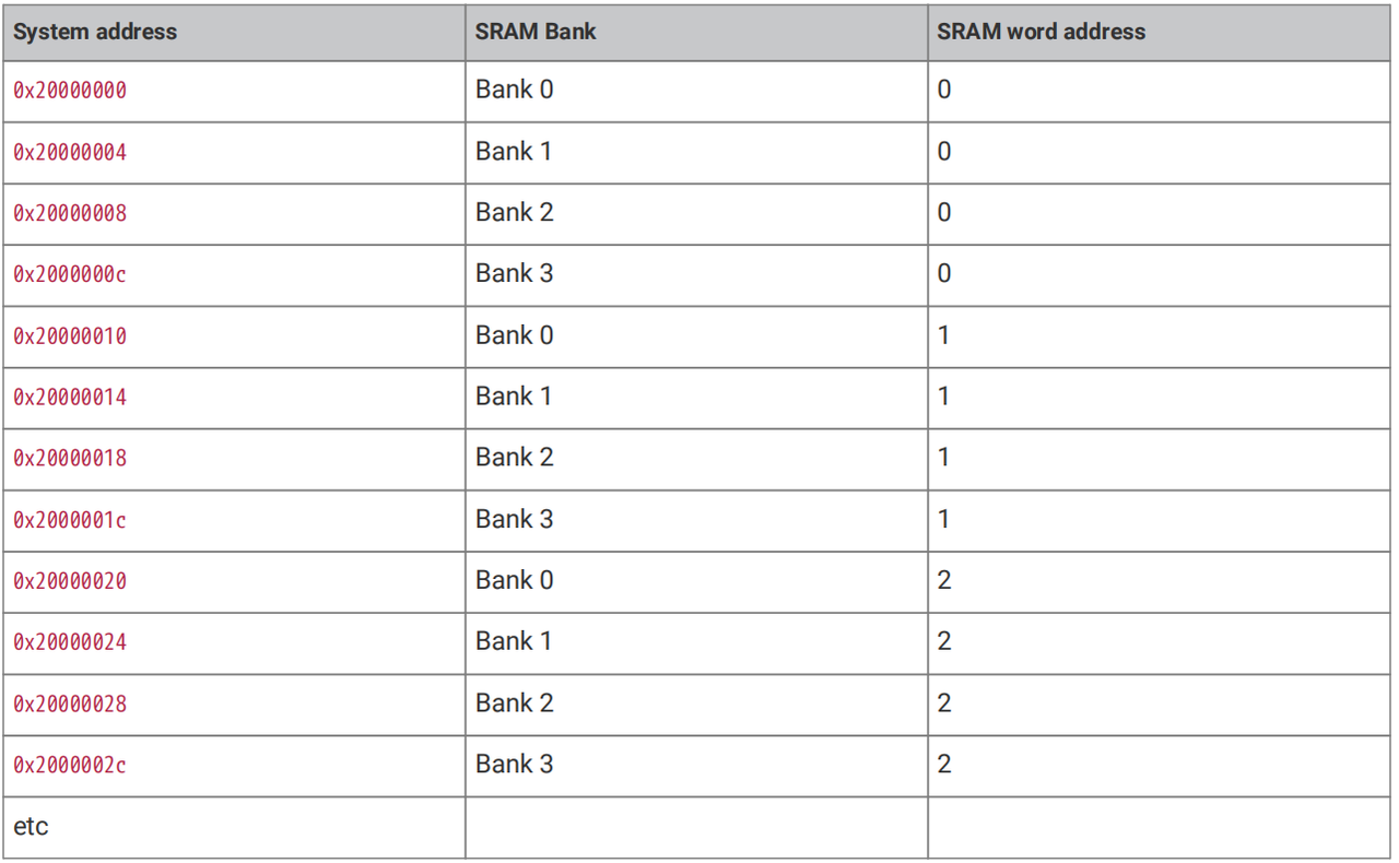
Figure 2.19 RP2040 SRAM Bank System Address to Word Address Mapping Table
We can see that this mapping table contains the following information:
System address: The "house number" of SRAM, through which the CPU core or DMA accesses the SRAM (for example, 0x20000000 is the first house number of SRAM);
SRAM Bank (SRAM physical partition): the actual physical storage block of SRAM (Bank0 to Bank3 are shown here, and there are additionally 2 small 4kB banks);
SRAM word address: A "word" refers to 32 bits (equivalent to 4 bytes), and this address serves as the offset number within the corresponding bank (for example, "word address 0" corresponds to the first 32-bit data entry in the bank).
We can see that as the system address increments by 4 each time (since 32 bits = 4 bytes), different banks are polled in the order "Bank0 → Bank1 → Bank2 → Bank3", and then it returns to Bank0 to increment the "word address" — for example:
0x20000000 (house number) → Bank0, word address 0;
0x20000004 (+ 4) → Bank1, word address 0;
0x20000010 (plus 4) → return to Bank0, word address 1.
The advantage of this mapping is that when multiple modules access different system addresses simultaneously, they are actually accessing different physical banks. For example, when Core0 accesses 0x20000000 (Bank0) and DMA accesses 0x20000004 (Bank1), the two will not interfere with each other, realizing "parallel access" and greatly improving the read and write speed of SRAM.
In addition, there are two small 4kB banks in the SRAM (starting at address 0x20040000) that can be dedicated to the two cores (for example, for storing stack and frequently executed code) — since these are independent banks, core accesses will not be stalled by other modules, thus ensuring operational efficiency.
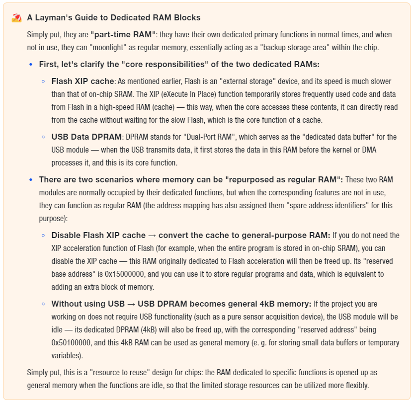
In addition to the on-chip SRAM, there are two dedicated RAM blocks available for use in certain scenarios:
If the flash XIP cache is disabled, the cache will start from 0x15000000
If USB is not in use, the USB data DPRAM can be used as a 4kB memory starting from 0x50100000.
3.Flash
Here, we first introduce two key concepts:
QSPI interface: a "high-speed data line" between the chip and external Flash (faster than ordinary SPI), which is responsible for the communication between the chip and the external Flash.
XIP (Execute In Place): Literally meaning "execute in place", it eliminates the need to copy programs from external Flash to on-chip SRAM, as programs can be run directly by accessing the external Flash, which effectively treats the external Flash as "expanded memory" and saves SRAM space.
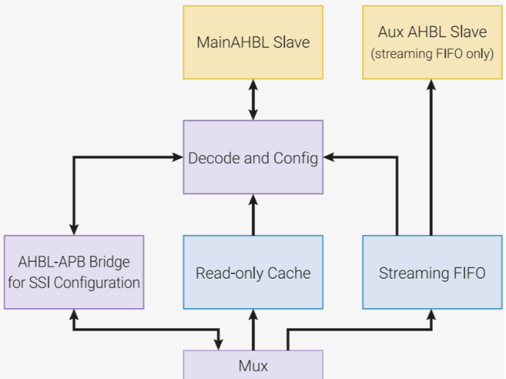
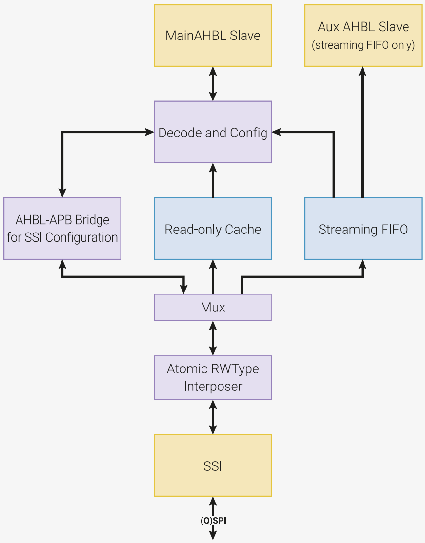
Figure 2.20 Block Diagram of RP2040 External Flash XIP (Execute In Place) hardware Architecture
The core of the entire structure is to enable external Flash to be accessed just like internal memory, accelerate the process with cache, and meanwhile ensure stable communication:
SSI Module: It directly connects to the QSPI interface and serves as the "physical layer" for communication with external Flash — it is responsible for transmitting and receiving QSPI signals, and is the component that actually transfers data with the external Flash.
Atomic RWType Interposer: It ensures that read and write operations on Flash are "completely uninterrupted"(for example, when reading a 32-bit data, the process will not be interrupted by other operations), so as to avoid data reading errors or writing confusion.
Mux Multiplexer: It acts as a "data path switch", selecting whether to read data from Cache or directly from Flash, with priority given to Cache for faster access.
Read-only Cache (Read-Only Cache): Since the speed of external Flash is lower than that of on-chip SRAM, the Cache stores frequently used content from the Flash (such as frequently executed program instructions) here; when the core accesses data, it first checks the Cache, and if the target content exists, it reads directly without waiting for the slow Flash, which greatly improves the speed of XIP.
Streaming FIFO Continuous Data Buffer: When a large volume of consecutive data (such as a lengthy program segment or a large file) is to be read from Flash, the data will first be stored in this FIFO before being transferred to the kernel, which prevents the data transmission from being intermittent and enables smoother consecutive access.
Decode and Config Address Resolution Configuration Unit:
Parse the address sent by the core: determine which location of the external Flash this address corresponds to;
Manage the configuration of the entire XIP hardware: such as enabling/disabling the Cache, setting the communication speed of QSPI, configuring the size of the FIFO, etc.
Main AHBL Slave / Aux AHBL Slave: This XIP hardware is connected to the "interface" of the system bus (AHBL):
Main Interface: responsible for regular Flash access (such as reading scattered instructions/data);
Aux Interface: exclusively responsible for high-speed continuous data transmission of Streaming FIFO, and is specifically designed for high-traffic scenarios.
AHBL-APB Bridge for SSI Configuration: It serves as the configuration interface of the SSI. The core sets parameters (such as the clock frequency and transmission mode of QSPI) for the SSI module via the APB bus, enabling the SSI to communicate with external Flash of different models in a compatible manner.
When the kernel needs to read program instructions from the external Flash:
The kernel sends the address to Decode and Config, and parses out which location in the Flash it corresponds to;
The Mux first checks the Read-only Cache: if the content corresponding to this address exists in the Cache, it is directly returned to the kernel;
If the data is not available in the Cache, the SSI module will read it from the external Flash via QSPI.
The read-back data is first stored in the Cache (to facilitate subsequent reads) and simultaneously passed to the kernel;
When reading a long continuous sequence of instructions, the data will first be stored in the Streaming FIFO and then transferred to the kernel in batches.
All in all, external Flash can be accessed via the QSPI interface using execute-in-place (XIP) hardware, which allows the system to address and access external flash memory in the same way as accessing internal memory.