



Getting Started with Embedded ADC: Analog‑Digital Signals & Peripheral Basics
Beginner‑friendly embedded tutorial explaining analog‑digital signals, ADC internal structure, workflow and key performance parameters.
- Analog Signals and Digital Signals
Signals can be divided into digital signals and analog signals according to continuity and discreteness.

Figure 1‑1 Analog signals and digital signals
Analog signal An analog signal is a continuous‑time signal whose amplitude can take infinitely many values at any time point. It can change seamlessly over time and can represent physical phenomena in the real world. For example, sound, light intensity and temperature are all analog signals.
Digital signal A digital signal is a discrete‑time signal with only a limited set of values, typically 0 and 1. Digital signals are represented in binary form, which makes them especially suitable for computers and digital electronic systems. All data processed inside computers are digital signals. For instance, music stored on CDs or transmitted via streaming services is converted into digital signals consisting of sequences of 0 and 1. Image files such as JPEG and PNG exist as digital signals during storage and transmission, with each pixel represented by numeric values.
Differences between the two: analog signals are continuous and can take arbitrary values in time and amplitude; digital signals are discrete and can only take a finite set of values.
‑ Analog signals are more susceptible to noise and interference, while digital signals have better noise immunity since only two states (0 and 1) need to be distinguished. ‑ Digital signals are easier to store and transmit and can be precisely copied by digital circuits. Analog signals may suffer distortion during copying and transmission.
Analog data from external sensors must be converted into digital signals by an ADC (Analog‑to‑Digital Converter) before processing and transmission inside computers.
For example, imagine you are making a phone call with a friend. Your voice is continuously‑changing analog signal. For telephone transmission, it needs to be converted into digital signals understandable by computers, namely binary numbers made of 0 and 1. Your voice is sampled by the phone; each small segment is converted into digital bits of 0 and 1 and transmitted to the recipient’s phone. The receiving phone converts those digital bits back into analog signals so your friend can hear your voice.

Computers can only recognize and process digital signals. Analog signals collected by sensors require conversion to digital form before computer processing. An ADC samples your voice at fixed time intervals and converts each segment into digital codes composed of 0 and 1. These digital codes are the “digital version” of your voice and can be easily transmitted in the digital domain. At the receiving end, a DAC (Digital‑to‑Analog Converter) converts those digital codes back into sound so your friend hears a nearly identical copy of your speech.
- Introduction to ADC Peripheral
An Analog‑to‑Digital Converter (ADC) is an electronic device that converts analog signals into digital signals. It is widely used in electronic equipment such as sensor interfaces, audio processing and measuring instruments, and plays a critical role in modern electronic design.

Figure 1‑3 Schematic diagram for analog‑to‑digital conversion principle of ADC
ADCs appear in nearly all electronic devices requiring analog‑to‑digital conversion. Common applications include:
Audio equipment Convert sound signals into digital form for processing and storage inside microphones, audio recorders and digital audio players.
Sensor interfaces Convert analog outputs from temperature, pressure, light‑intensity and other sensors into digital signals for data processing and control.
Data‑acquisition systems Use ADC to sample analog signals for monitoring and analysis in laboratory and industrial control scenarios.
Communication systems Digitize analog signals for modulation, encoding and transmission in radio communications.
Image processing Use ADC to convert optical signals into digital signals for image processing and storage inside cameras and image sensors.
2.1 Basic Structure and Working Principle of ADC
The basic building blocks of an ADC are listed below:
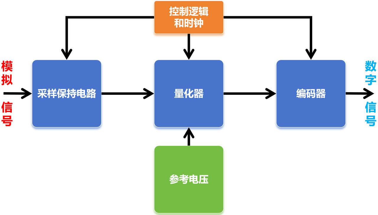
Sample and Hold Circuit The sample‑and‑hold circuit samples the continuous analog input at specific time instants and holds that instantaneous voltage value until the next sampling instant. A stable input is required during ADC conversion to produce accurate digital outputs.
Quantizer The quantizer divides the held voltage from the sample‑and‑hold circuit into several discrete voltage levels corresponding to possible digital outputs. Quantization introduces quantization error, which occurs when an analog value cannot map exactly to one digital value and produces certain distortion.
Encoder The encoder translates quantized discrete voltage levels into binary codes, i.e. digital signals. This step maps input‑signal amplitude onto a fixed set of binary numbers.
Reference Voltage The reference voltage defines the full‑scale quantization range, specifying maximum and minimum input voltages the ADC can handle. Input signals are quantized against this reference voltage to generate proper binary outputs.
Control Logic and Clock Control logic manages ADC operations including sample timing and conversion triggering. The clock synchronizes each step so sampling, holding, quantization and encoding execute sequentially.
The fundamental function of an ADC is to convert continuously‑varying analog signals such as voltage into a sequence of discrete digital values. Its workflow generally consists of three steps:
- Sampling Discretize the analog signal in time by taking samples at fixed time intervals. Sampling frequency determines the highest signal frequency the ADC can capture. According to the Nyquist theorem, sampling frequency must be at least twice the signal bandwidth.
- Quantization Convert sampled analog values into discrete voltage levels. The number of quantization levels is determined by ADC resolution. For example, an 8‑bit ADC has 256 quantization levels.
- Encoding Translate quantized signal levels into binary codes for digital‑system processing and storage. The bit width of the encoded result equals the ADC resolution.
We will use the AD conversion process for a sine wave as an example to illustrate ADC workflow.
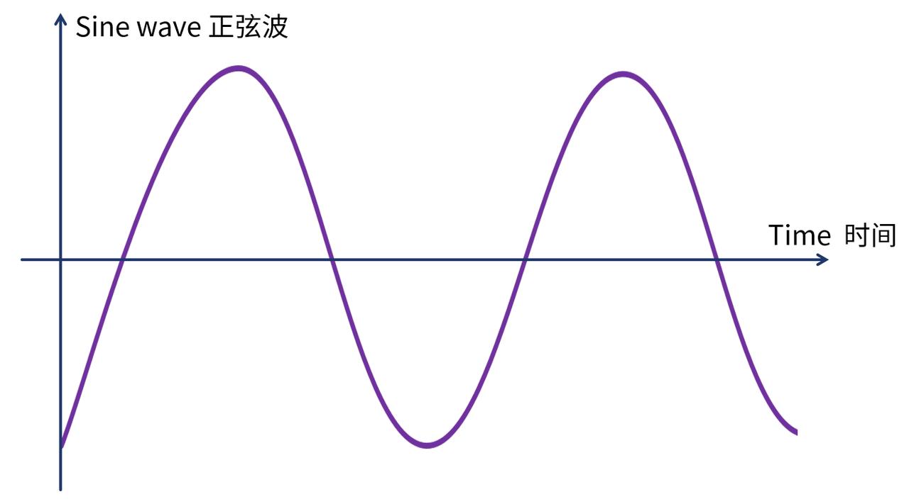
Figure 1‑5 Sine‑wave AD conversion example waveform diagram
This target signal is continuous in both time and amplitude. The analog signal feeds into a sample‑and‑hold circuit built around a sampling switch. The sampling switch toggles open and closed at the sampling frequency. When closed, the signal amplitude at that instant appears at the switch output and is held.
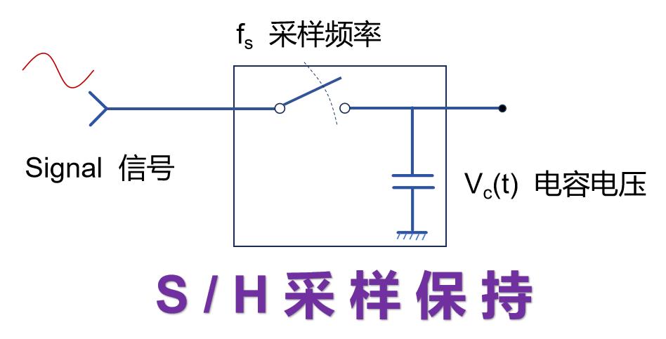
Figure 1‑6 Schematic of sample‑and‑hold circuit
The hold function is implemented by a capacitor connected to the output of the sampling switch. When the switch closes, the capacitor charges to the analog‑signal voltage at that moment. When sampling completes and the switch opens, the capacitor maintains that sampled‑signal voltage until the next sampling instant.
Waveform showing capacitor voltage (sampled signal) versus time:
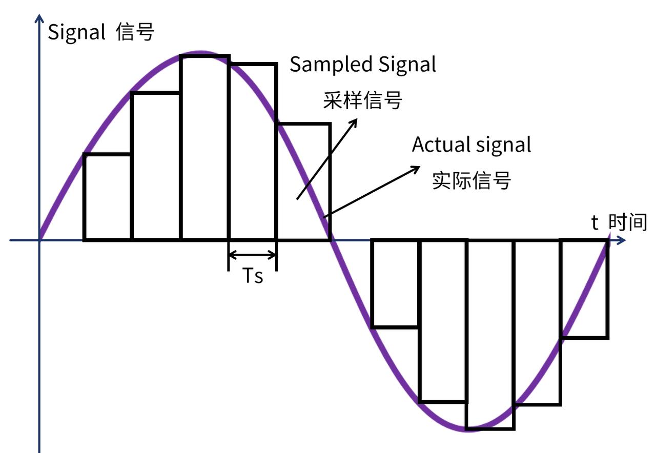
Figure 1‑7 Waveform comparison between sampled signal and original signal: the capacitor voltage forms rectangular pulses whose height equals the signal amplitude at the start of each sampling interval. Amplitude becomes discrete while time remains continuous. The voltage across the capacitor is passed onward for further processing.
It is obvious that sampling cannot perfectly reproduce signal amplitude. Noticeable error exists between sampled voltage and original sine wave. This error is inherent during sampling, though it can be reduced by raising sampling frequency. However, excessively high sampling frequency increases processing and memory requirements.
Figure 1‑8 Amplitude‑error comparison for ADC sampling process: obvious error (purple filled region) between sampled‑voltage bars (black) and original sine‑wave signal (purple).
Capacitor voltage is then fed to the quantizer. As shown above, capacitor output appears as time‑continuous rectangular bars with constant amplitude inside each sampling interval. The quantizer partitions those held voltages into discrete levels; in simple terms, each rectangular‑bar voltage within a sampling interval gets mapped to a binary number composed of 0 and 1.
Assume we have a 3‑bit ADC with 0 V to 1 V input range. The full voltage range maps onto eight 3‑bit binary numbers from 000 to 111. Its resolution is calculated as:
$$ \frac{1,\text{V}}{2^3} = 0.125,\text{V} $$
With 0.125 V resolution, any input amplitude between 0 V and 0.125 V produces digital output 000; voltages between 0.125 V and 0.250 V map to 001; amplitudes between 0.250 V and 0.375 V map to 010. The corresponding transfer curve for this conversion is shown below:
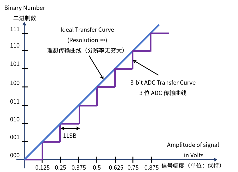
Figure 1‑9 Comparison of transfer curve and ideal curve for a 3‑bit ADC
Quantization error appears in this process. For instance, all analog amplitudes from 0 V to 0.125 V yield the identical 000 code. This causes information loss because every value inside that 0‑0.125 V window is represented by the same digital output. Quantization error can be reduced by decreasing the resolution voltage, i.e. adding more output bits for the same input‑voltage span.
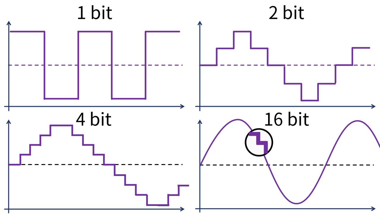
Figure 1‑11 Waveform comparison showing quantization error for different ADC bit widths
Finally, the encoder converts quantized discrete levels into binary codes, producing the final digital signal.
2.2 ADC Performance Specifications
When selecting and using an ADC, pay attention to these key parameters:
Resolution The bit width of ADC binary output determines conversion precision. Higher resolution means more quantization levels and finer output results. Common resolutions are 8‑bit, 10‑bit, 12‑bit, 16‑bit, etc.
Sampling Rate Number of analog‑signal samples taken by the ADC per unit time. Sampling rate defines the maximum signal frequency the ADC can handle. Unit: Samples Per Second (SPS).
SNR (Signal‑to‑Noise Ratio) Ratio between desired input signal and noise components present in ADC output. Higher SNR means better noise immunity and cleaner output signal.
ENOB (Effective Number of Bits) Represents real‑world effective resolution of the ADC, taking SNR and non‑linearity errors into account. Higher ENOB indicates performance closer to ideal behaviour.
THD (Total Harmonic Distortion) Measures harmonic components introduced by non‑linear distortion within ADC output. Lower THD corresponds to better linearity.
DNL (Differential Non‑Linearity) Deviation of voltage difference between adjacent quantization steps from ideal step size. DNL impacts ADC accuracy and resolution.
INL (Integral Non‑Linearity) Maximum deviation between real ADC transfer curve and ideal straight‑line transfer characteristic. INL also affects measurement accuracy.
Input Range Voltage span of analog input signals that the ADC can convert correctly. Signals exceeding input range introduce errors.
Power Consumption Electrical power consumed while the ADC operates. Power consumption is especially important for battery‑powered portable devices.
2.3 ADC Classifications
From the perspective of integration with microcontroller hardware, ADCs fall into on‑chip integrated ADC and external ADC chip categories.
On‑chip integrated ADC An on‑chip ADC is built‑inside a microcontroller or SoC. No extra external interface circuitry is required, occupying little PCB area. It features low power consumption, fast response and low cost. Restricted by die size, power budget and noise environment, on‑chip ADC generally achieves lower resolution and precision than external ADC chips. Typical on‑chip ADC resolution ranges from 8‑bit to 12‑bit.
External ADC chip External ADC chips often deliver higher resolution (16‑bit, 24‑bit or above) and superior measurement precision to satisfy high‑accuracy requirements. Designers may select appropriate external ADC devices such as high‑speed sampling ADC or low‑speed high‑precision ADC according to application requirements. Better power‑supply and signal‑noise isolation can be achieved. Drawbacks include extra external connecting circuitry, increased PCB complexity and footprint, considerations for interface drive capability and signal integrity, as well as relatively higher power consumption.
In short, on‑chip integrated ADC fits ordinary sensor data acquisition, simple audio‑signal processing and low‑cost portable‑device projects. External ADC chips are used in high‑precision measuring instruments, high‑speed data‑acquisition systems, audio‑video processing and professional medical equipment demanding high resolution and accuracy.
Classified according to operating principles, ADCs can be divided into multiple types:
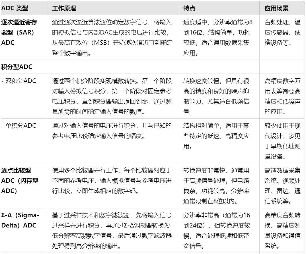
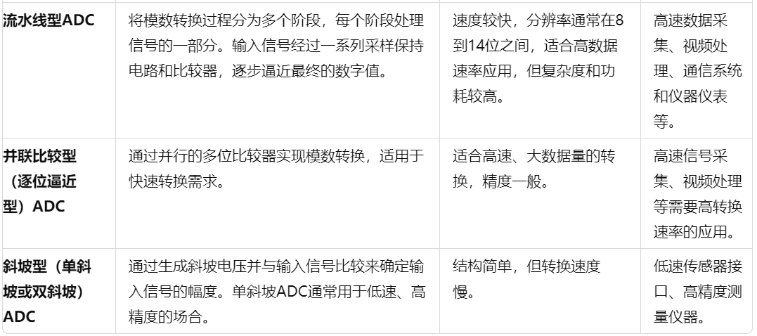
Each ADC type has unique operating principles and suitable application scenarios. Selecting the correct ADC type matching project requirements is critical for efficient data acquisition and processing.