Full Analysis of RP2040 Pinout: Pin Mapping Is the Chip's "Wiring Guide"
This article explains pin mapping and its vital roles in hardware design, coding and resource allocation using RP2040 as an example.
COMPONENTS
PROJECT DESCRIPTION
Pin Mapping
When it comes to chip learning, pin mapping serves as the critical link between "internal chip functions" and "actual physical hardware" — it acts as a "wiring guide" that creates a one-to-one correspondence between functional modules in the chip block diagram (such as GPIO, ADC, UART) and the physical pins on the chip package (i. e., the exposed metal leads of the chip).
The reason why it is necessary to understand the pin mapping is as follows:
It serves as the "operation manual" for hardware design: the block diagram tells you that the chip has functions such as GPIO and ADC, but the pinout will clearly specify "which physical pins on the chip these functions correspond to specifically" — for example, if you want to connect a temperature and humidity sensor (using I2C) to the RP2040, you have to find the physical pins that support the I2C function through the pinout before you can solder and wire correctly;
It serves as the "function index" for program development: when writing a program to control a certain function (such as turning on an LED), you need to determine the "pin number corresponding to that function" through pin mapping, so as to correctly configure the pin in the code;
It serves as a "reference sheet" for function to reuse: many pins support multiple functions (for example, the GPIOx of RP2040 supports ADC at the same time), and the pin mapping marks the to reuse function of each pin, making it convenient for you to select the appropriate pin according to the requirements of your project.
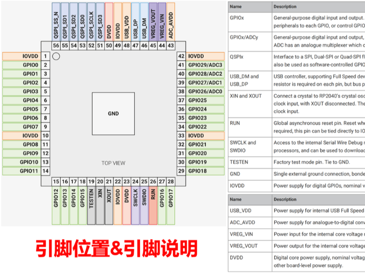
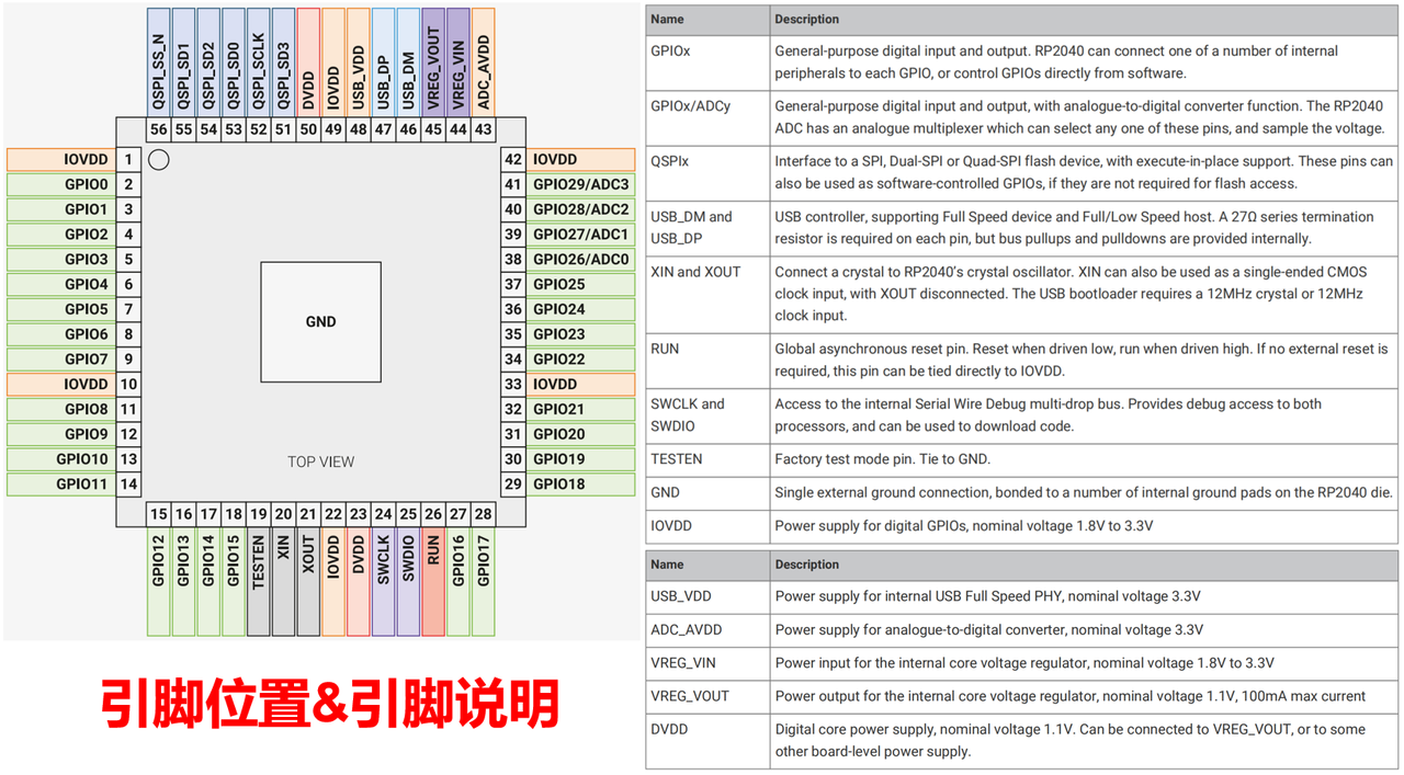
Figure 2.5 Pin Mapping and Function Description Diagram of RP2040 Chip
Take the pinout diagram of the RP2040 as an example: the left side of the diagram shows the physical pin numbers of the chip, while the right side lists the corresponding functions of each pin (for instance, GPIO029/ADC3 means "physical pin 42 corresponds to the GPIO29 function and supports ADC3 sampling at the same time"). Only by mastering this can you translate the "GPIO and ADC functions" you learned from the block diagram into practical hardware connections and program development — this is also a necessary step when learning any chip, moving from "architecture understanding" to "practical application".