From Pipeline to Low Power: How Cortex-M0+ Became the "King of Cost-Effectiveness" for Microcontrol
This article details the Cortex-M0+ core adopted by RP2040, including its main features, supporting modules and applicable embedded scenarios.
COMPONENTS
PROJECT DESCRIPTION
Cortex-M0+ Core
The core is the central processing brain of a microcontroller chip, and all program execution, data computation, and task scheduling of the chip are ultimately completed by the core, which directly determines the core capability boundaries of the chip (such as computing speed, power consumption level, and supported functions), serving as the basis for judging "what scenarios the chip is suitable for"(e. g., low-power devices / complex computing devices) and "what tasks it can perform".
The ARM Cortex-M0+ processor is an ultra-low-power, low-cost microprocessor that supports the ARMv6M instruction set.
The chip has the following features:
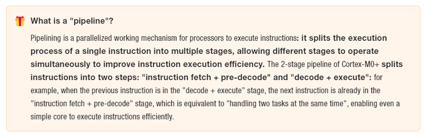
It adopts a 2-stage pipeline structure (instruction fetch + pre-decoding, decoding + execution);
Single-cycle I/O access is supported:
"Single cycle" means that when accessing peripherals such as GPIO, a read or write operation can be completed in only one clock cycle;
With extremely fast IO access speed and ultra-low response latency, it is suitable for scenarios that impose high requirements on IO timing, such as quickly controlling LED blinking and outputting high-frequency signals.
Low power consumption with integrated sleep mode:
Sleep mode is a state in which the processor "temporarily suspends operation and reduces energy consumption": the core will turn off some circuits, lower the clock frequency, and only retain the necessary wake-up detection function.
Significantly reducing power consumption when chips are in idle state is a core requirement for battery-powered devices such as smart bracelets and wireless sensors.
Capabilities of determinism, fixed latency, and interrupt handling:
"Determinacy" means that the interrupt response time is fixed: regardless of what the processor is currently doing, the latency for processing an interrupt (the time from receiving the interrupt signal to starting to execute the interrupt service routine) will not vary erratically.
In real-time systems (such as industrial control and motor speed regulation), it can ensure that urgent tasks (e. g., sensor triggering) receive timely and stable responses, and will not cause failures due to delay fluctuations.
Thumb-2 Technology:
Thumb-2 is an instruction set technology developed by ARM, which combines 16-bit short instructions and 32-bit long instructions (standard ARM instructions are 32-bit);
It not only reduces the code size (as 16-bit instructions occupy less space) but also retains the execution efficiency of 32-bit instructions, striking a balance between "code storage footprint" and "execution speed".
32-bit single-cycle hardware multiplier:
A "hardware multiplier" is a hardware module in a chip that is specifically dedicated to multiplication operations (as opposed to "software multiplication", which simulates multiplication via code); the term "single-cycle" means that a single multiplication of 32-bit numbers can be completed in just one clock cycle. ;;
It significantly accelerates multiplication operations (software-based multiplication may take more than ten cycles), making it ideal for scenarios requiring fast computation, such as data filtering and simple mathematical operations.
The C application binary interface compatibility exception model allows the use of pure C functions as interrupt handlers:
The "exception model" refers to the rules for handling unexpected events such as interrupts and faults; this feature allows developers to write interrupt handlers in C language (without having to write low-level assembly code);
It significantly reduces the development difficulty of interrupt programs, allowing ordinary developers (who do not need to be proficient in assembly language) to easily write interrupt logic.
Input from low-power sleep modes using Wait For Interrupt (WFI), Wait For Event (WFE) instructions, or the interrupt-on-exit sleep return function:
This is the trigger method for entering the "low-power sleep mode":
WFI (Wait For Interrupt): After execution, the core enters a sleep state and will only be woken up upon receiving an interrupt signal;
WFE (Wait For Event): After execution, the core enters a sleep state and will not be woken up until an event signal is received;
It enables developers to flexibly control the chip to enter a low-power state, further reducing power consumption during idle periods and extending the battery life of battery-powered devices.
Commonly used in the following applications:
General data processing and I/O control tasks
Ultra-low power applications
Update/Replacement of 8-bit/16-bit Microcontrollers
Low-cost ASIC and ASSP
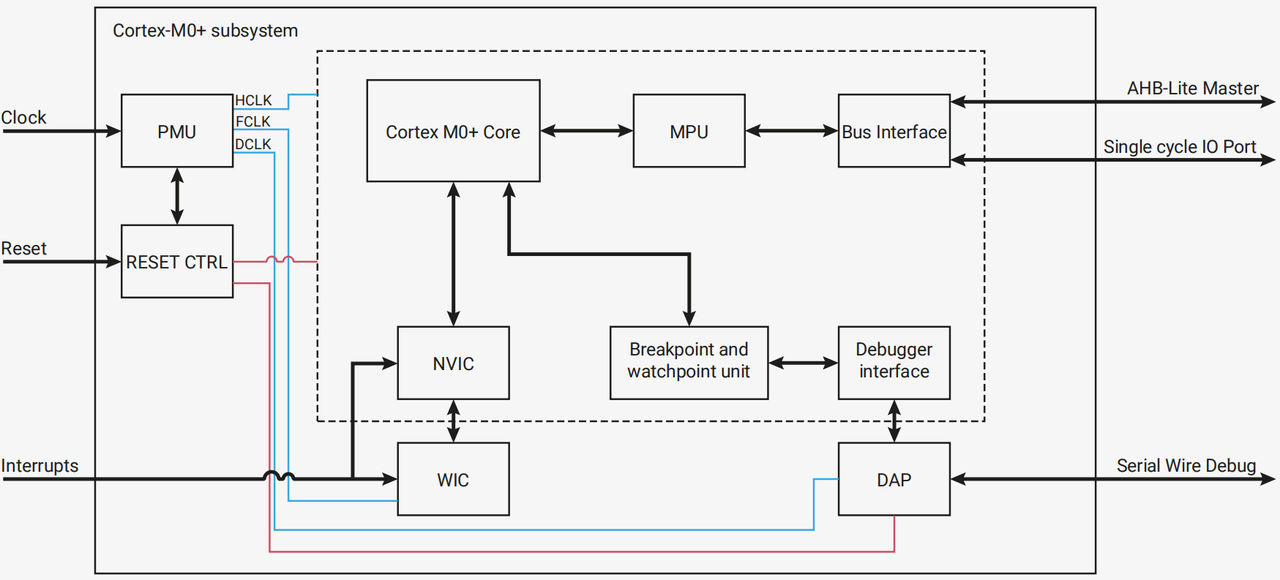
The block diagram of the system unit is as follows:
Figure 2.16 Architecture Block Diagram of System Units for ARM Cortex-M0+ Core
It can be seen that for the kernel to operate properly, different modules are required to provide fundamental support such as power supply, clock, interrupt and debugging for the kernel, so as to ensure its stable operation:
Power Consumption and Clock PMU: It provides the kernel with various clock signals (HCLK/FCLK/DCLK) and controls the power consumption status of the kernel (such as reducing the clock frequency or powering off during sleep), serving as the core module for realizing "ultra-low power consumption".
Reset Control (RESET CTRL): It is responsible for restarting the core. When the program freezes or the chip malfunctions, it triggers a reset to return the core to its initial state for re-operation.
Memory and Access MPU + Bus Interface:
MPU (Memory Protection Unit): It manages the memory access permissions of the kernel, prevents programs from erroneously accessing illegal memory (for example, applications accessing memory exclusive to the kernel), and improves system stability;
Bus Interface: serves as the "bridge" for communication between the core and other modules of the chip (such as SRAM and peripherals) — the core reads memory and controls peripherals through it.
Interrupts and Low-Power NVIC + WIC:
Nested Vectored Interrupt Controller (NVIC): Manages interrupt requests (IRQ), schedules interrupt priorities, and enables the core to respond to urgent tasks in a timely manner;
Wake-up Interrupt Controller (WIC): It acts as a "sleep wake-up module" — when the kernel is in deep sleep, regular interrupts cannot wake it up, but the WIC can detect interrupt signals and pull the kernel back from the low-power state to the working state.
Debug Breakpoint/Watchpoint Unit + DAP:
Breakpoint/Watchpoint Unit: The "handle" for debugging programs — breakpoints suspend the kernel when it executes the specified code, while watchpoints suspend the kernel when it accesses the specified memory/registers, facilitating the identification of program bugs;
DAP (Debug Access Port): it serves as the entry point for external debuggers (such as a computer) to communicate with the core, and enables control over the core's operation and inspection of its status via the SWD (Serial Wire Debug) interface.