



Embedded DDS AD9833: Datasheet, Driver, SPI & Frequency Calculation
AD9833 DDS driver & SPI analysis
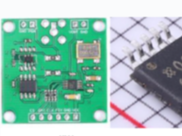
AD9833 is a low‑power digital waveform generator (DDS) chip manufactured by Analog Devices. It is designed for applications requiring precise frequency and phase control and can generate sine, triangle and square‑wave signals. AD9833 is commonly used in signal sources and test‑equipment projects.
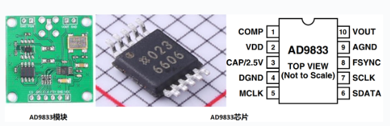
Key features:
Frequency and phase programmability Frequency range: 0 MHz to 12.5 MHz Phase programmability: supports precise phase‑adjustment for output signals
Power consumption Only 20 mW power draw under 3 V supply.
Resolution 28‑bit frequency register delivers frequency resolution as fine as 0.1 Hz with a 25 MHz reference clock. With a 1 MHz reference clock, resolution reaches 0.004 Hz.
Output waveforms Supports sine‑wave, triangle‑wave and square‑wave outputs.
Power‑supply requirements Operating supply‑voltage range: 2.3 V to 5.5 V.
Interface 3‑wire SPI communication interface supporting clock rates up to 40 MHz, compatible with standard DSP and micro‑controller peripherals.
Power management SLEEP power‑down function. Unused internal blocks can be shut down to save power. For example, the DAC block can be disabled while clock‑signal generation remains active.
- AD9833 Basic Architecture
Block diagram of AD9833:
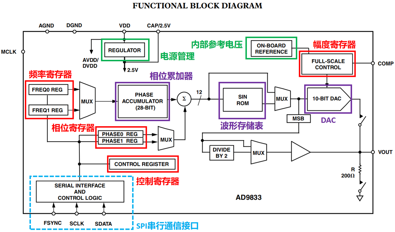
Internal block descriptions:
Frequency registers (FREQ0 REG and FREQ1 REG): Set frequency of the generated output signal.
Phase registers (PHASE1 and PHASE0): Generate phase values for waveform synthesis.
Multiplexers (PHASE MUX and FREQ MUX): Select outputs from frequency‑register and phase‑register banks.
Phase accumulator: 28‑bit digital accumulator. It continuously adds frequency‑control words (from FREQ0 REG / FREQ1 REG) on each clock cycle.
Waveform lookup table: Stores amplitude sample values used for waveform reconstruction.
DAC Digital‑to‑Analog Converter: 10‑bit DAC that converts digital samples into analog output signals.
Power‑management unit (REGULATOR and ON‑BOARD REFERENCE): Includes voltage regulator and internal 2.5 V voltage reference.
Full‑scale‑control amplitude register: Adjusts output‑signal amplitude level.
Serial‑interface and control‑logic block: Provides serial‑communication interface and chip‑wide configuration logic.
- AD9833 Electrical Specifications
AD9833 electrical‑parameter table:
Parameters are grouped into four categories:
Signal‑output‑related parameters The integrated DAC is 10‑bit. Maximum sample rate is 25 MSPS. Output voltage ranges from 38 mV up to 0.65 V. Output voltage varies with temperature with a temperature coefficient of 200 ppm/°C. Linearity errors include ±1.0 LSB Integral Non‑Linearity and ±0.5 LSB Differential Non‑Linearity.
DDS signal‑generation‑related parameters Signal‑to‑Noise Ratio: 55 ~ 60 dB. Total Harmonic Distortion ranges from −66 dBc to −56 dBc. Spurious‑Free Dynamic Range (SFDR): −60 dBc for wide‑band measurements; −78 dBc within the narrow ±200 kHz observation window.
SPI‑communication‑related parameters Input high‑level and low‑level thresholds change with supply voltage. Input high‑level VINH: 1.7 V ~ 2.8 V. Input low‑level VINL: 0.5 V ~ 0.8 V. Maximum input current IINH / IINL equals 10 mA. Input pin capacitance is 3 pF.
Power‑supply‑related parameters Supply‑input voltage: 2.3 V ~ 5.5 V. Typical active‑mode operating‑current: 4.5 mA ~ 5.5 mA. In sleep mode with DAC disabled while MCLK remains active, supply current drops to 0.5 mA.
- AD9833 Pin‑out and SPI Communication Parameters
3.1 AD9833 Pin Description
AD9833 pin‑assignment diagram:
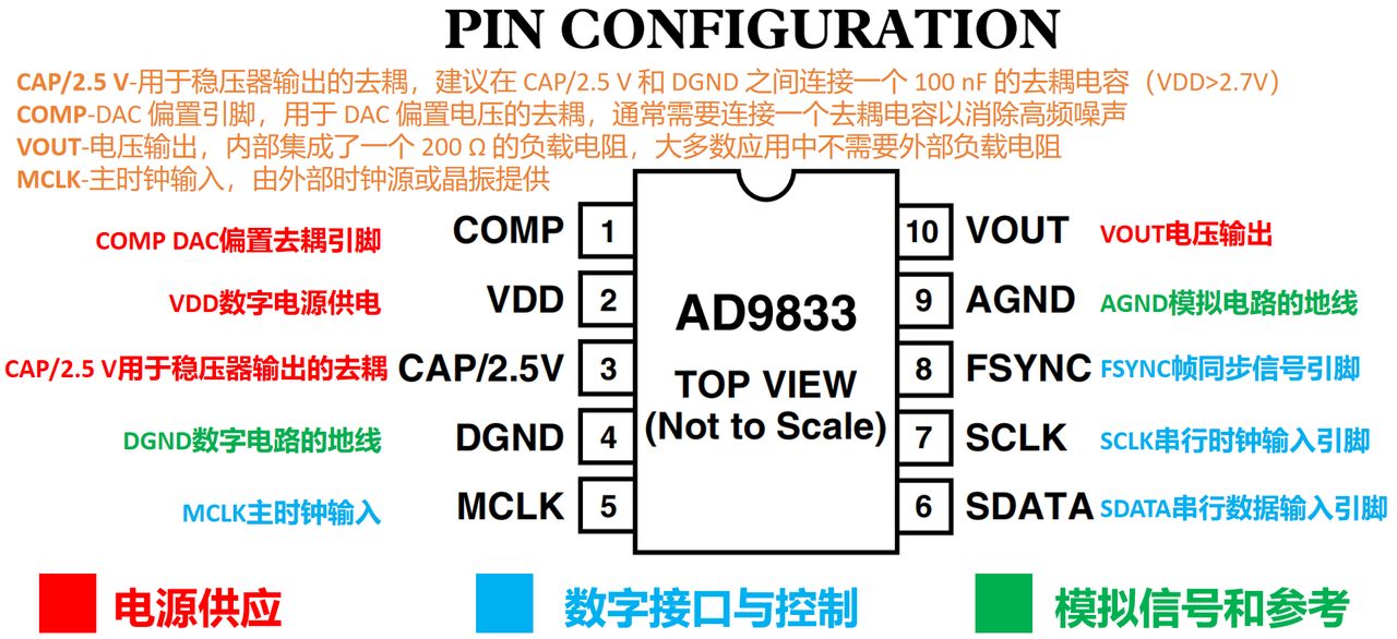
Pin‑number and function table:
3.2 AD9833 SPI Electrical Timing and Communication Flow
SPI timing‑characteristic table:
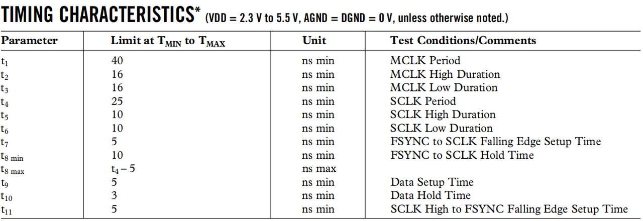
Definition of each timing parameter:
SPI timing‑sequence diagram:
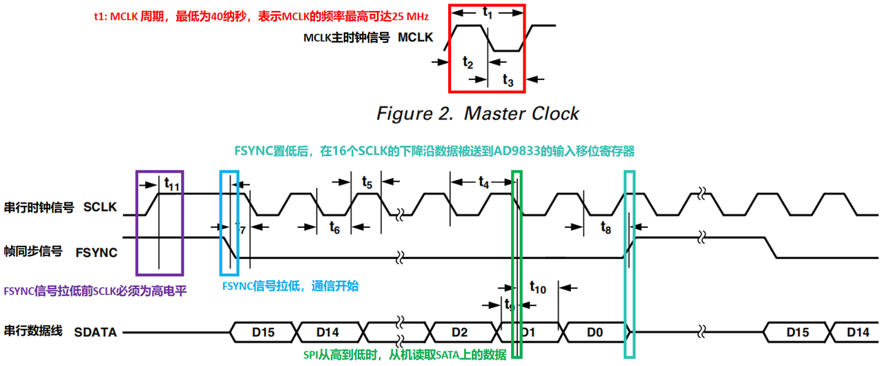
Definition of four main signals and timing parameters:
Master clock signal MCLK is the main input clock for AD9833 and sets overall system speed. Minimum MCLK period t1 is 40 ns, corresponding to maximum 25 MHz clock frequency. Minimum high‑level duration t2 and low‑level duration t3 are each 16 ns.
Serial‑clock signal SCLK is the serial clock controlling data sampling and transfer. One bit of SDATA is transferred per SCLK cycle. Minimum complete SCLK period t4 is 25 ns, so maximum SPI clock rate reaches 40 MHz. Minimum SCLK high‑time t5 and low‑time t6 are both 10 ns.
Frame‑sync signal FSYNC marks the start of a data frame. Minimum setup time t7 from FSYNC falling edge to first SCLK falling edge is 5 ns. Hold‑time t8 from last SCLK falling edge to FSYNC rising edge is minimum 10 ns and maximum (t4 − 5 ns).
Serial‑data line SDATA carries serial‑bit stream. Data setup time t9 from stable SDATA to SCLK falling edge ≥ 5 ns. Data hold‑time t10 from SCLK falling edge until SDATA change ≥ 3 ns. Setup‑time t11 from SCLK high to FSYNC falling edge ≥ 5 ns.
AD9833 uses 3‑wire SPI with host controller. Communication sequence:
- Communication start
- Host pulls FSYNC low to activate communication; AD9833 is ready to receive data.
- Host generates SCLK clock to drive data‑transfer timing.
- Data transmission
- After FSYNC goes low, AD9833 input shift register accepts bits. Each SCLK falling edge shifts one bit from SDATA into the chip.
- Full 16‑bit packet transmission requires 16 SCLK clock cycles.
- Data hold and end‑of‑transmission
- After completing 16‑bit transfer, FSYNC may be pulled high to terminate one frame.
- For successive multi‑packet transfers, keep FSYNC low and stream multiple 16‑bit words. FSYNC is pulled high only after the 16th SCLK falling edge of the final packet.
- After loading new register values, allow 7‑8 MCLK cycles before output waveform updates accordingly.
Important note: AD9833 SPI uses CPOL = 0, CPHA = 1 (SPI Mode 1). Unlike standard SPI chip‑select, FSYNC is asserted briefly before each frame; SCLK only runs while FSYNC stays low. This protocol resembles variants used by I²S, TDM and certain DSP peripherals.
In short: before every write transaction you must drive SCLK high manually, then assert the frame‑sync pin low before starting data communication.
- AD9833 Device Control
4.1 AD9833 Control Register
AD9833 contains one 16‑bit control register for configuring operating modes.
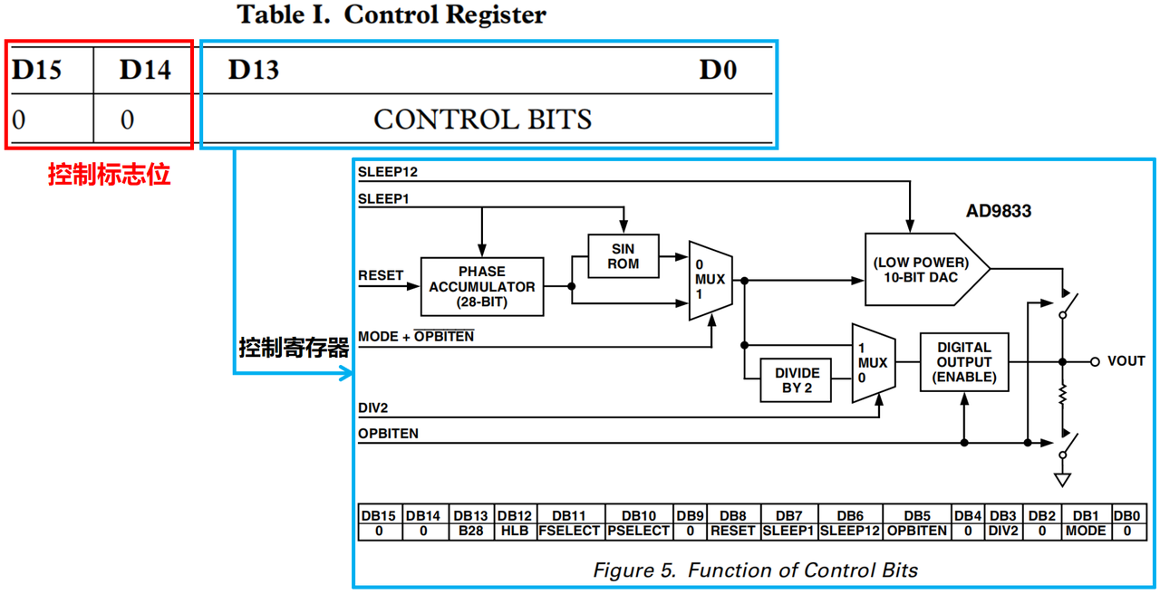
The register contains flag and control bits. When modifying control‑register content, the two highest bits D15 and D14 must both be written as zero.
Bit‑field definition for control register:
Brief bit‑function summary:
D13 (B28): Frequency‑register write mode control B28 = 1: full 28‑bit frequency word is written over two consecutive transactions. B28 = 0: allows separate writes to upper 14 bits (MSB) or lower 14 bits (LSB).
D12 (HLB): Select high‑14‑bit or low‑14‑bit frequency‑register segment. Valid only when B28 = 0.
D11 (FSELECT): Select frequency‑register source for phase accumulator. 0 = FREQ0, 1 = FREQ1.
D10 (PSELECT): Select phase‑register source for phase‑accumulator output. 0 = PHASE0, 1 = PHASE1.
D8 (RESET): Resets all internal registers to zero; analog output holds mid‑scale value. When RESET = 0 waveform generation commences.
D7 (SLEEP1): SLEEP1 = 1 disables internal MCLK; DAC output freezes at present level.
D6 (SLEEP12): SLEEP12 = 1 powers‑down the on‑chip DAC block.
D5 (OPBITEN): Works together with D1 (MODE) to configure VOUT behaviour. When OPBITEN = 1, VOUT is disconnected from DAC reconstruction output and instead outputs either MSB or MSB/2 of DAC raw data. Bit D3 (DIV2) selects which variant.
D3 (DIV2): Used jointly with OPBITEN. DIV2 = 1: output MSB directly onto VOUT pin. DIV2 = 0: output MSB/2 onto VOUT pin.
D1 (MODE): Combined with OPBITEN for VOUT configuration. MODE = 1: bypass SIN ROM and produce triangle‑wave output. MODE = 0: route phase values through SIN ROM for sine‑wave generation.
All write transactions begin by writing to the control register. The two most‑significant bits of each 16‑bit word determine target register. Typical initialization workflow for AD9833:
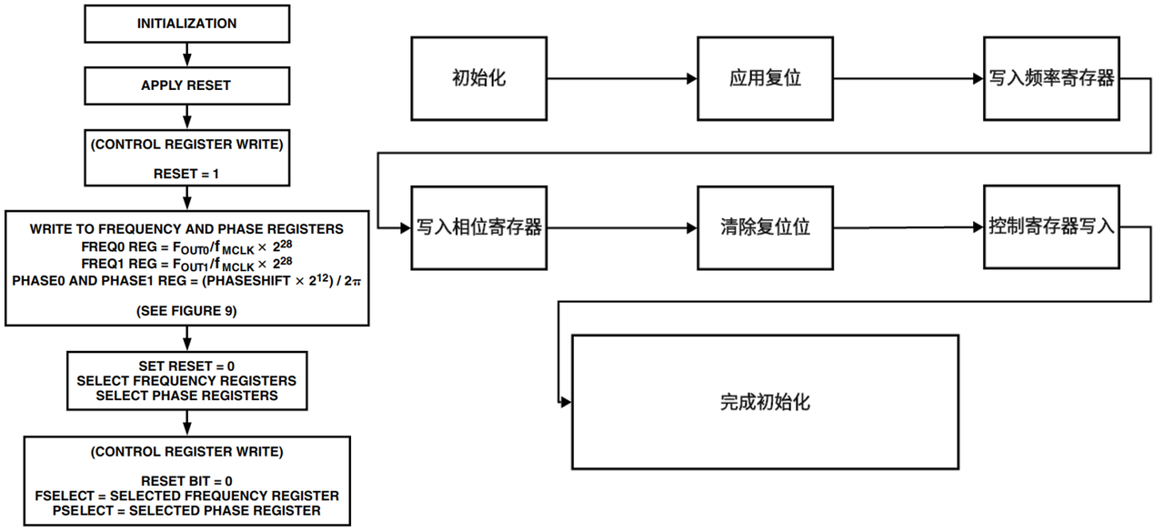
- Power‑on reset: Assert RESET bit to 1 after power‑up to guarantee known initial state for frequency, phase and control registers.
- Register configuration: Program control‑register bits. After finishing control‑register setup (control‑address bits set to '00'), configure other registers to select output waveform (sine / triangle / square), then program frequency‑register and phase‑register values (using appropriate control‑address bit combinations).
- Enable output: Clear RESET bit to start waveform generation.
4.2 AD9833 Frequency and Phase Registers
AD9833 includes two frequency registers and two phase registers to govern output‑signal frequency and phase.
- Frequency registers
- FREQ0 (28‑bit): Selected when FSELECT = 0. Sets output frequency proportional to MCLK clock.
- FREQ1 (28‑bit): Selected when FSELECT = 1. Sets output frequency proportional to MCLK clock.
- Phase registers
- PHASE0 (12‑bit): Selected when PSELECT = 0. Its value is added to phase‑accumulator output to produce phase offset.
- PHASE1 (12‑bit): Selected when PSELECT = 1. Its value is added to phase‑accumulator output for phase offset adjustment.
Write‑sequence diagram for frequency and phase registers:
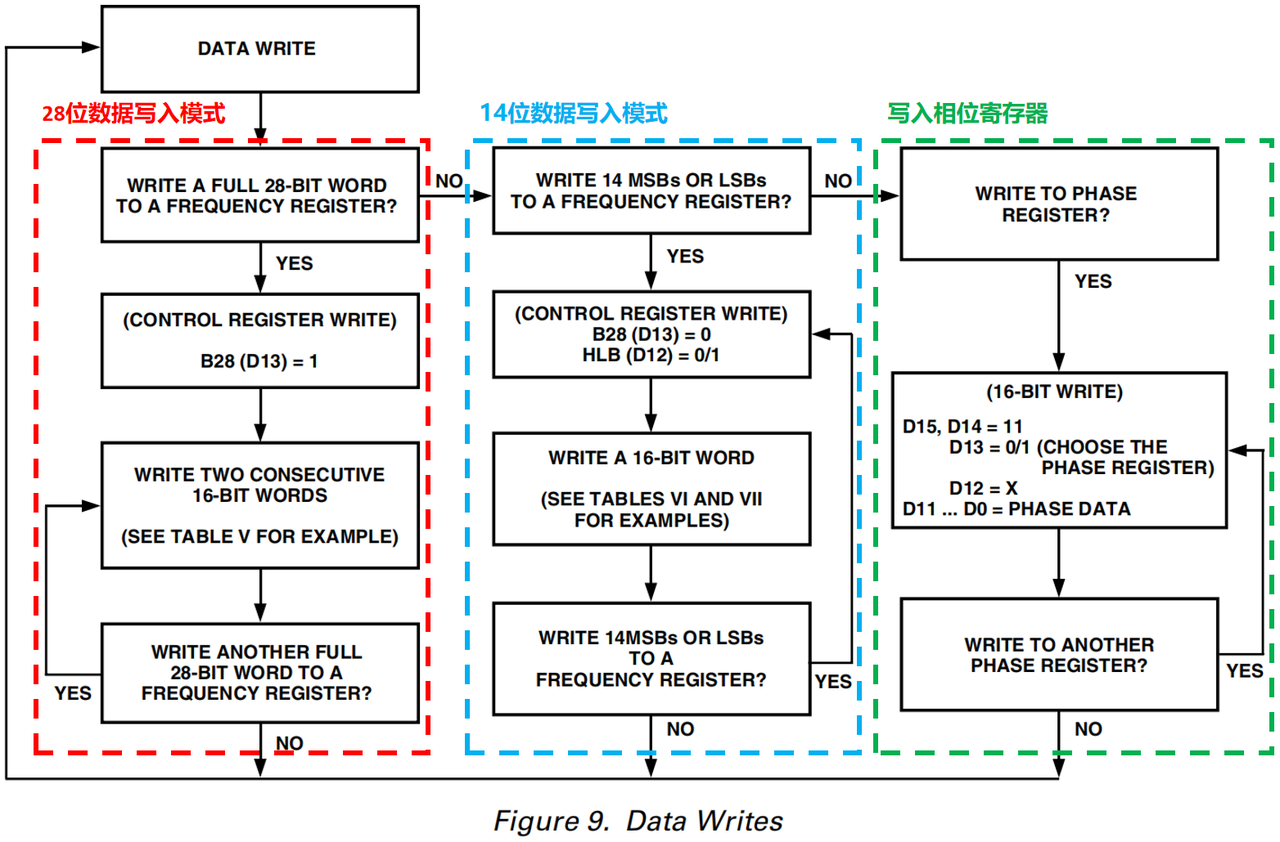
Two available write modes for frequency registers: 14‑bit partial‑write mode and full 28‑bit write mode. Configure B28 (D13) and HLB (D12) in control register to choose mode, then transmit frequency data. Afterwards program phase register: set D15 and D14 bits in control word to indicate phase‑register target, use D13 bit to pick PHASE0 or PHASE1, then send phase value.
4.2.1 Writing to frequency registers
Frequency registers store 28‑bit binary numbers defining output frequency. Frequency formula: $$ f_{\text{OUT}} = \frac{f_{\text{MCLK}}}{2^{28}} \times \text{FREQREG} $$
Where FREQREG = content of selected frequency register; fMCLK = master‑clock frequency; fOUT = generated output frequency.
Because SPI transfers 16‑bit words per transaction, loading a complete 28‑bit frequency register requires two write operations. Set control‑word bit B28 (D13) = 1 for full‑28‑bit writes. Write sequence:
- Step 1: transmit lower 14 bits of frequency word.
- Step 2: transmit upper 14 bits of frequency word.
Partial‑update mode: set B28 = 0. The 28‑bit register acts as two independent 14‑bit segments: upper‑MSB 14 bits and lower‑LSB 14 bits. Modify MSB‑segment for coarse frequency tuning; modify LSB‑segment for fine frequency tuning.
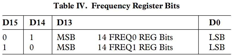
Control‑word D15 / D14 select target frequency register:
D15 = 0, D14 = 1: write to FREQ0 register, modify MSB 14‑bit segment. D15 = 1, D14 = 0: write to FREQ1 register, modify LSB 14‑bit segment.
4.2.2 Writing to phase registers
Phase‑offset formula: $$ \text{Phase offset} = \frac{2\pi}{4096} \times \text{PHASEREG} $$
PHASEREG represents value stored in selected 12‑bit phase register.
For phase‑register writes both D15 and D14 inside control word must equal 1. Bit D13 selects target register:
D13 = 0: write to PHASE0 register. D13 = 1: write to PHASE1 register.
4.3 AD9833 Sleep Function and Low‑Power Registers
Sleep capability is controlled via dedicated bits inside control register to shut‑down partial or full internal hardware for power saving. SLEEP1 and SLEEP12 bits determine which functional blocks remain powered.
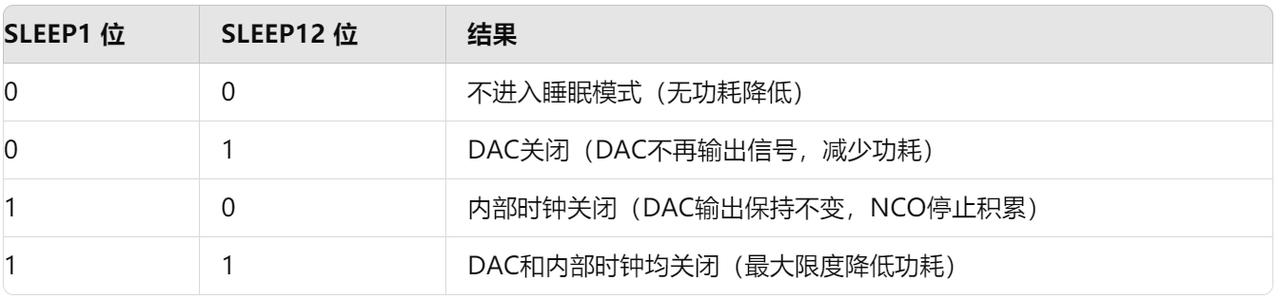
When SLEEP1 = 0, SLEEP12 = 1: DAC block is powered‑down. Suitable for applications only requiring MSB bit output.
When SLEEP1 = 1, SLEEP12 = 0: internal MCLK clock is disabled; NCO phase accumulation halts and DAC output holds static value. New frequency / phase / control words can still be written into registers. After clearing SLEEP1 bit MCLK resumes; register changes take effect after internal latency.
4.4 AD9833 Output Modes
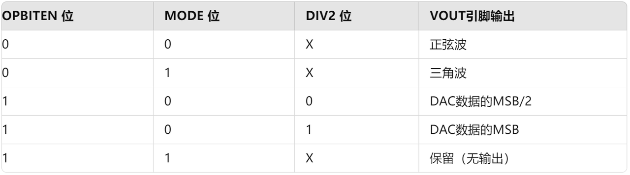
VOUT pin can output MSB bit stream, sine‑wave or triangle‑wave signals. Output behaviour is determined by OPBITEN (D5), MODE (D1) and DIV2 (D3) bits inside control register.
Important notes for waveform output:
‑ Sine‑wave / triangle‑wave amplitude range is 38 mV ~ 650 mV. Square‑wave maximum amplitude reaches 3.3 V. To achieve larger sine / triangle swing an external op‑amp amplifier stage is required; a digital potentiometer may be added for amplitude adjustment.
‑ Maximum output waveform frequency is 12.5 MHz derived from Nyquist sampling theorem. AD9833 maximum input MCLK is 25 MHz. To faithfully reconstruct a periodic signal sampling rate must be at least twice signal frequency, so each output cycle needs minimum two samples, yielding maximum output frequency = half MCLK = 12.5 MHz.
When adding digital potentiometers for amplitude control pay attention to potentiometer bandwidth. Limited‑bandwidth pots such as AD5260, X9C103, AD5292 (~1 MHz bandwidth) degrade high‑frequency signal amplitude. For signals approaching 10 MHz use high‑frequency variable‑gain amplifiers e.g. AD8367 (500 MHz bandwidth) instead.
4.4.1 Square‑wave / DAC MSB output
Set OPBITEN (D5) = 1. VOUT outputs MSB bit stream which forms square‑wave clock signal. DIV2 (D3) bit chooses whether square‑wave frequency is divided‑by‑two.
4.4.2 Sine‑wave output
To generate sine‑wave on VOUT: set MODE (D1) = 0 and OPBITEN (D5) = 0. Phase data passes through SIN ROM for amplitude lookup before feeding into DAC.
4.4.3 Triangle‑wave output
For triangle‑wave output set MODE (D1) = 1. SIN ROM is bypassed; raw truncated NCO digital values go directly to DAC to produce linear 10‑bit triangle‑wave.
Important: For any waveform‑output mode SLEEP12 bit must be 0 to keep DAC block enabled so analog signal can drive VOUT pin.