DS1302 RTC Hands‑on Guide: Features, Registers, Timing & PCB Layout
Practical embedded RTC tutorial covering DS1302 features, registers, communication timing and PCB layout design.
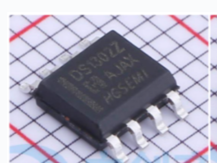
DS1302 is a widely‑used real‑time clock (RTC) chip. It keeps track of time including seconds, minutes, hours, day‑of‑week, date, month and year, and supports leap‑year compensation up to year 2100. It is commonly used in electronic projects requiring accurate time logging, such as data loggers, clocks, timers and automation systems.
Main characteristics are as follows:
Low power consumption In backup mode, DS1302 draws very low supply current, making it suitable for battery‑powered applications.
Serial interface It uses a simple three‑wire serial interface for data communication, reducing pin count requirements.
On‑chip RAM It contains 31‑byte internal RAM for user‑data storage.
Dual‑power supply design Supports primary power and backup power, so the clock continues running when main power is disconnected.
Temperature‑compensated timing Paired with an external crystal oscillator, DS1302 achieves good time accuracy, with typical accuracy of ±1 second per day.
Calendar functions Counts seconds, minutes, hours, date, weekday, month and year with leap‑year compensation. The clock supports either 24‑hour format or 12‑hour format with AM/PM indication.
Wide operating supply‑voltage range 2.0V ~ 5.5V.
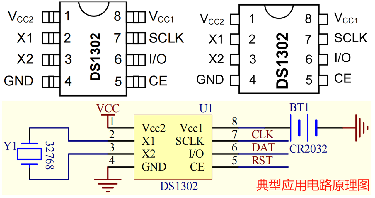
DS1302 communicates with microcontrollers via three wires: I/O data line, SCLK clock line and RST reset line. A typical application schematic is shown below:
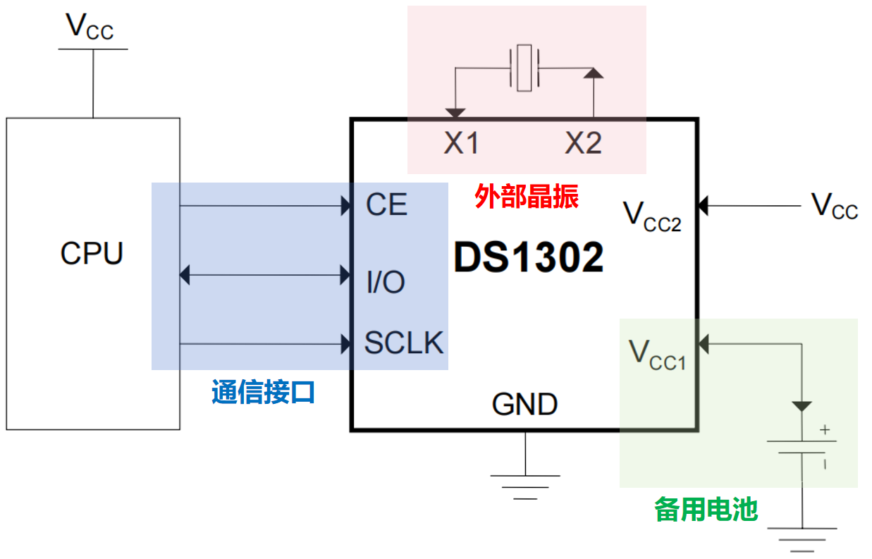
Generally, VCC2 of DS1302 is connected to a CR2032 coin‑cell battery to maintain clock operation after main power fails. In addition, DS1302 requires an external crystal oscillator, typically a 32.768 kHz passive crystal, to provide stable clock signals.
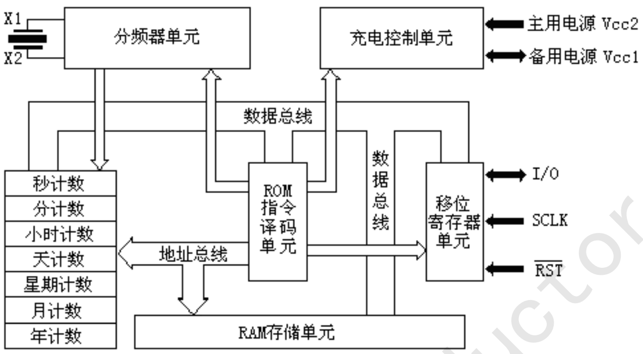
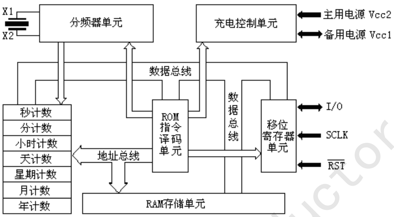
The above is the internal block diagram of the DS1302 chip. Its core functional unit consists of multiple counters. Driven by clock signals from the divider block, these counters track seconds, minutes, hours, date, month and year. The on‑chip RAM can store non‑volatile user data to retain status across system restarts.
DS1302 pin definitions and typical application circuit schematic:
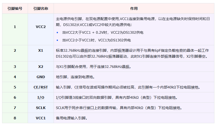
Pin names and functions are listed below:
DS1302 uses command bytes to control data read and write operations. Command‑byte format and functions:

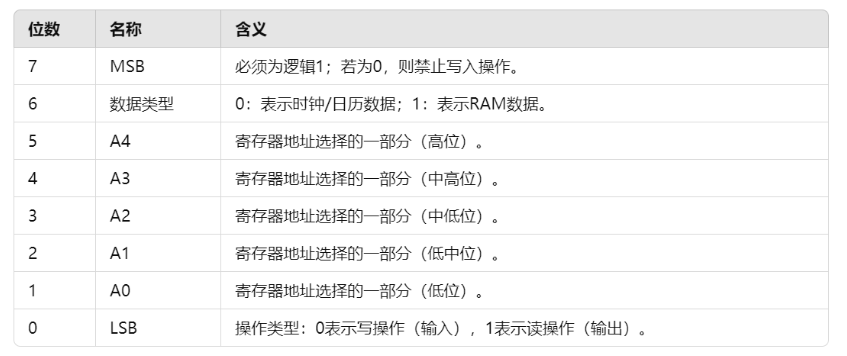
When communicating with the DS1302 chip, first pull the RST signal line high. Under each SCLK clock pulse, the shift register serially receives an 8‑bit command byte coming from the I/O pin. Received command bytes undergo serial‑to‑parallel conversion inside the shift register. Converted command bytes are sent to the ROM instruction decoder, which parses the command byte to determine the target internal register address and read‑write direction.
After the 8 SCLK cycles used for sending the command byte from the microcontroller, the DS1302 outputs 8 data bits over the following 8 SCLK cycles:
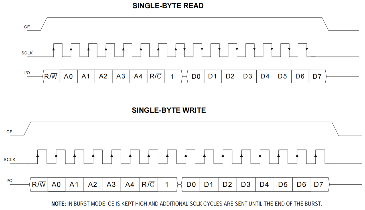
When the CE pin is high, all data transmission is enabled. CE also controls shift‑register access and terminates data transfers. Input data must be valid on the rising edge of SCLK, while output data is driven on the falling edge. On power‑up, CE must stay low. When driving CE high, the SCLK pin must be held low.
Continuous SCLK pulses allow burst read/write of multiple bytes, up to 248 bytes total, for calendar‑clock registers or RAM locations. Burst mode is activated by setting address bits 1‑5 to logic 1. Within burst mode, bit 6 selects target memory type (clock/calendar or RAM), and bit 0 defines read‑or‑write direction.
Write clock‑calendar registers In burst‑write mode, you must write the first eight registers sequentially (address 0 to 7). Clock‑calendar registers form a contiguous data structure; incomplete writes may result in inconsistent time values.
Write RAM registers For RAM registers, you do not need to write all 31 bytes. Only bytes requiring updates need to be written.
DS1302 internal register definitions and addresses:
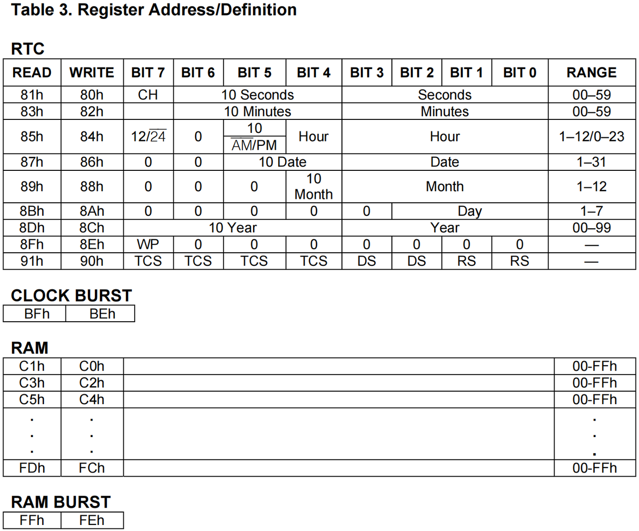
Registers are grouped as below:
Clock‑calendar registers Store time‑and‑date information with addresses from 81h to 8Dh. Fields include seconds, minutes, hours, date, month, weekday and year. Each field is split into tens‑digit and units‑digit sub‑fields. For the seconds field, there are 10 Seconds (tens digit) and Seconds (units digit). DS1302 uses Binary‑Coded‑Decimal (BCD) format for time‑and‑date storage. For example for time “12:34:56”, register values are: seconds(56) = 01010110, minutes(34) = 00110100, hours(12) = 00010010.
Seconds register field Bit 7 is the clock‑halt bit. When set to logic 1, the crystal oscillator stops and DS1302 enters low‑power backup mode with supply current below 100 nA. Writing bit 7 to logic 0 restarts the clock oscillator.
Hours register field DS1302 supports 12‑hour or 24‑hour mode selected by bit 7 of the hours register. Hour values must be re‑initialized every time you toggle between 12‑hour and 24‑hour modes. When bit 7 = 1: 12‑hour mode, bit 5 indicates AM/PM status. When bit 7 = 0: 24‑hour mode, bit 5 acts as an additional tens‑hour bit for values 20‑23.
Control register The control register (8Fh) implements write‑protection. Bit 7 is the write‑protect bit. Logic 1 disables writes; logic 0 enables write operations to protect on‑chip data. The WP bit must be cleared before attempting any write operations to the device.
Trickle‑charge register The trickle‑charge register (91h) configures the trickle‑charging circuit. Only pattern 1010 enables the trickle charger; all other patterns disable it. This register manages safe and effective battery charging during main‑power loss and is seldom used in common applications, so detailed description is omitted here.
On‑chip RAM DS1302 provides 31‑byte RAM registers from address C0h to FDh for arbitrary user‑data storage. Each RAM byte ranges from 00h to FFh.
Clock‑calendar burst register Clock‑calendar burst mode enables sequential read/write of multiple registers to simplify data transfer. Starting from bit 0 of address 0, you can read or write the first eight clock‑calendar registers consecutively.
RAM burst register RAM burst mode supports sequential read/write for up to 31 RAM bytes. Data transfers start from bit 0 of address 0 without needing individual register accesses.
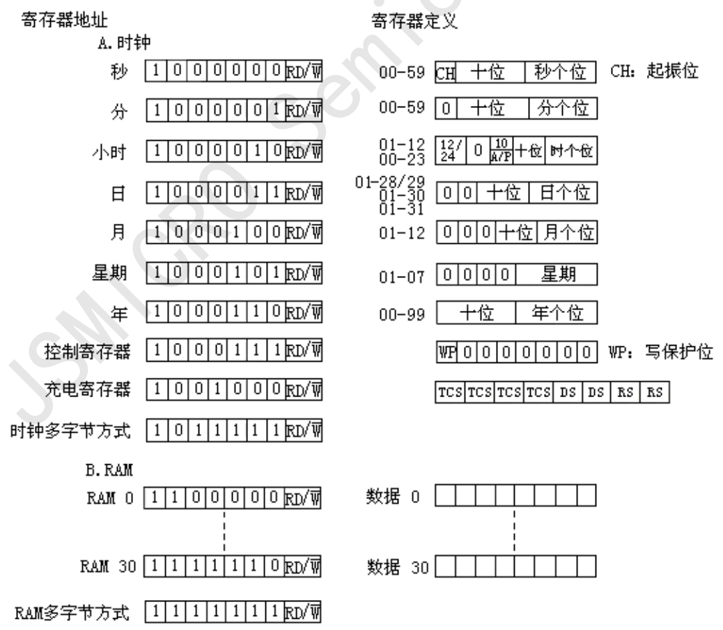
Register addresses correspond to bits 7 through bit 1 inside the command byte, as shown below:
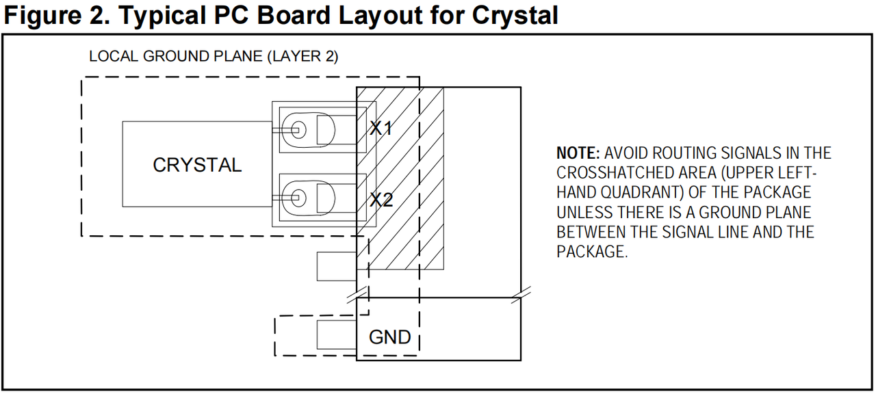
When laying out PCB traces for the DS1302 external crystal oscillator, apply guard‑ring grounding layout: surround crystal signal traces (X1 and X2 pins) with ground copper to form a ground guard‑ring for suppressing electromagnetic interference.