



DS1232 Explained: Watchdog Timer & Power‑Monitor Unit
Detailed introduction for DS1232 supervisor chip, covering internal modules, watchdog timer and power‑supply monitoring working principle.
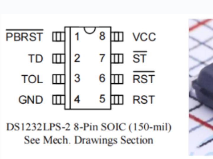
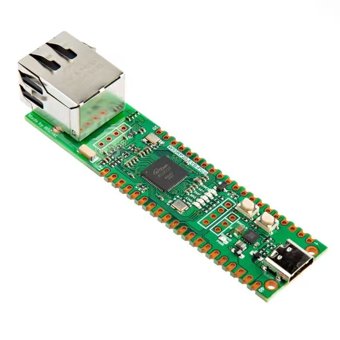
- DS1232 Chip Introduction
DS1232 is a microprocessor monitor chip released by Maxim.
Its main functions are as follows:
Watchdog‑timer function If the MCU does not feed pulse signals to the ST (strobe) pin within the specified time window, the chip generates a reset signal.
Power‑supply voltage monitoring and reset function When VCC supply voltage drops below the reset threshold (approx. 4.37V or 4.62V depending on part number), the chip automatically outputs a reset signal (RST).
Manual reset interface Users can connect an external push‑button to the PBRST pin to trigger manual reset.
Therefore, DS1232 is widely used in single‑chip microcontrollers and embedded systems requiring high reliability.
- DS1232 Pin Introduction
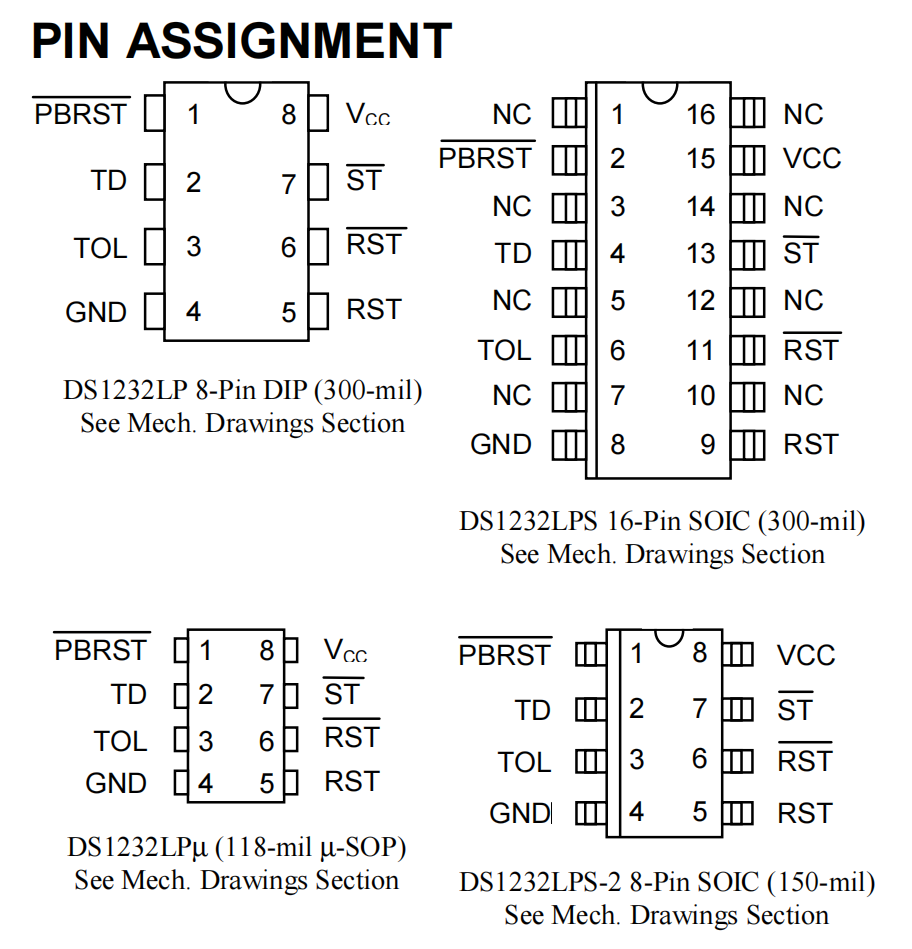
Pin‑out descriptions for DS1232 are shown in the table below:
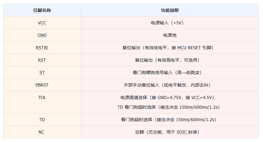
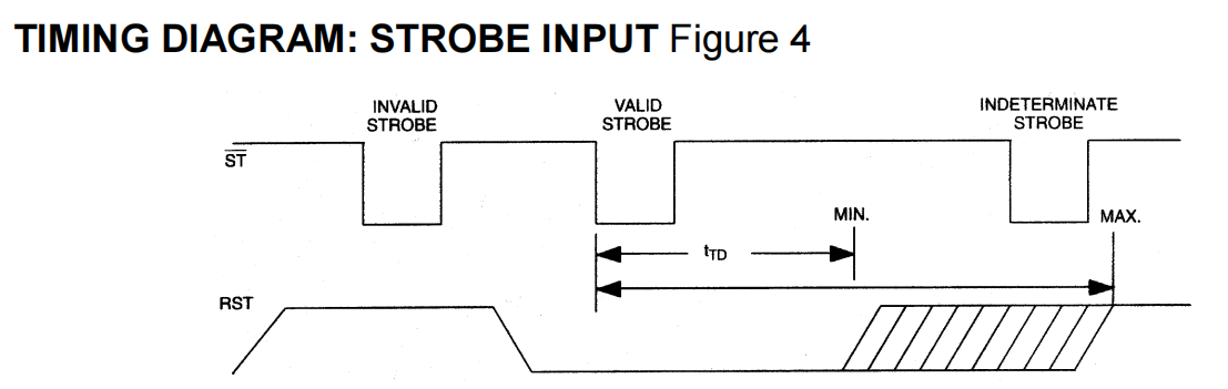
During system operation, the DS1232 requires continuous pulse sequences fed into the ST pin. Pulse interval is configured via the TD pin. If the pulse interval exceeds the value set by TD pin, the chip outputs reset pulses on the RST and /RST pins to reset the microcontroller. This function is commonly known as watchdog, and sending these trigger pulses is called “feeding the dog”.
- DS1232 Internal Structure and Working Principle
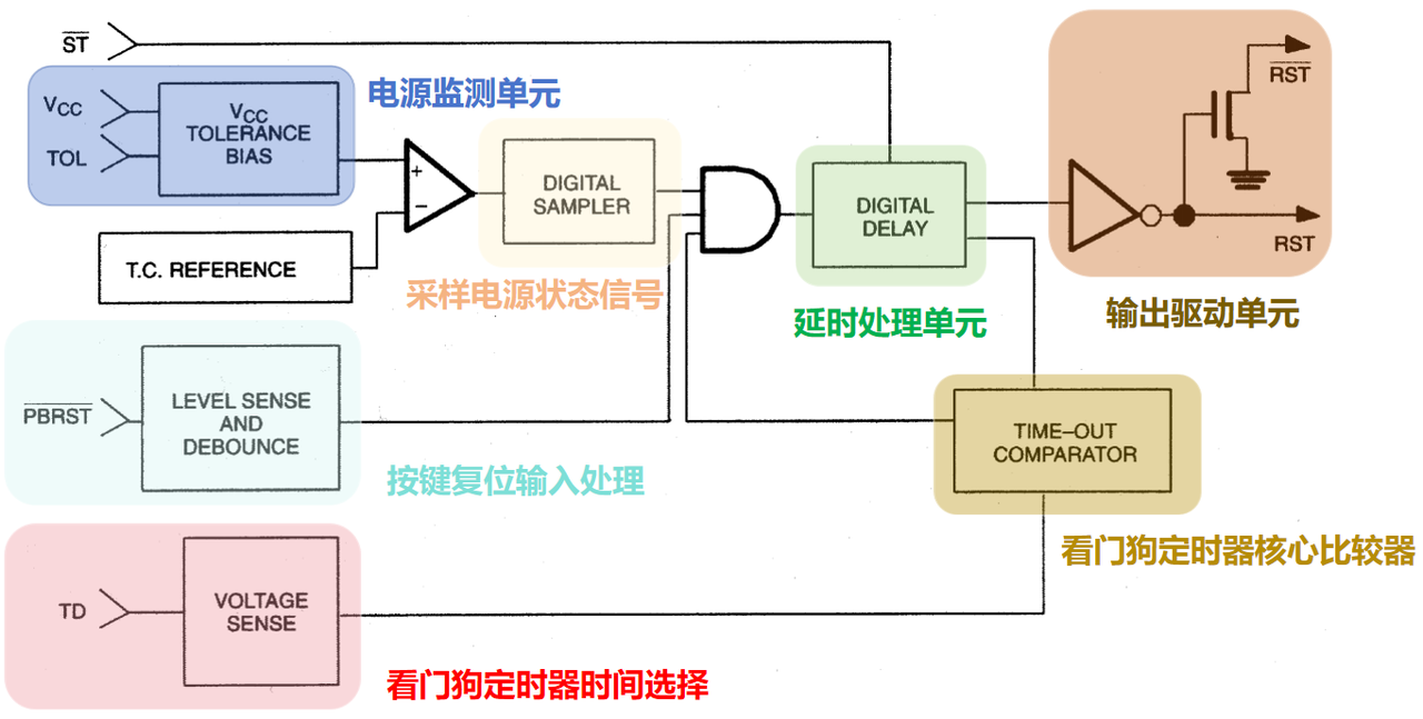
Internal modules of DS1232 are listed below:
Power‑supply monitoring unit (VCC Comparator + Reference + TOL) Detects whether power‑supply voltage is within normal range.
Principle: Compare VCC voltage against internal temperature‑compensated reference voltage. Threshold is selected by the TOL pin: TOL=GND: threshold 4.75V TOL=VCC: threshold 4.5V
Trigger condition: When VCC falls below threshold, signal propagates to subsequent logic and forces system reset.
Digital sampler for power‑status signal Digitally samples outputs from power comparator to filter transient interference, preventing false resets caused by power glitches or noise. Reset is triggered only when supply voltage stays below threshold continuously.
Push‑button reset input processing (Level Sense and Debounce, PBRST) Triggers manual system reset.
Principle: The PBRST pin connects to push‑button, triggered by low level. Internal circuit implements hardware debounce to avoid multiple false resets caused by mechanical switch bounce. After button release, reset output stays active for 250 ms to guarantee reliable MCU reset.
Watchdog timeout selection (Voltage Sense, TD)
Function: Sets watchdog timeout period.
Principle: Configured by hardware connection of TD pin: TD=GND: 150 ms TD=Floating: 600 ms TD=VCC: 1.2 s
MCU must send a falling‑edge pulse to the ST pin within this window (feed‑dog operation), otherwise reset will be asserted.
Watchdog timeout comparator core (Time‑Out Comparator) Judges whether MCU performs feed‑dog operation within allowed time.
Principle: If no falling‑edge event arrives on ST within configured timeout → MCU is regarded as hung → reset request is generated. Valid edge transition on ST → internal timer is cleared and restarts counting.
Digital delay unit (Digital Delay) Guarantees minimum duration of reset output pulses.
Principle: No matter reset source (power‑supply failure, push‑button reset or watchdog timeout), Digital Delay ensures reset output lasts for at least 250 ms, preventing abnormal MCU boot from too‑short reset pulses.
Output driver unit (Output Driver, RST/RST̅) Sends reset control signals to microcontroller.
Principle: Provides two complementary outputs: RST (active‑low) /RST (active‑high) Allows users to select reset polarity matching target MCU requirements.
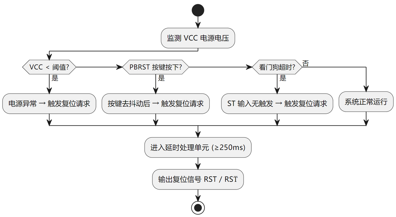
DS1232 monitors VCC voltage through its power‑monitoring unit. Reset is asserted immediately upon voltage fault, and reset signal is held for at least 250 ms after power recovers for system stability. It supports push‑button reset input; internal debounce also generates minimum 250 ms reset pulse. Its built‑in watchdog timer asserts automatic reset if no trigger pulse from processor arrives within configured timeout (150 ms / 600 ms / 1.2 s). All reset requests pass through digital‑delay block and are driven by output driver as RST//RST signals to deliver reliable reset control for microprocessors.
- Reference application circuit and notes
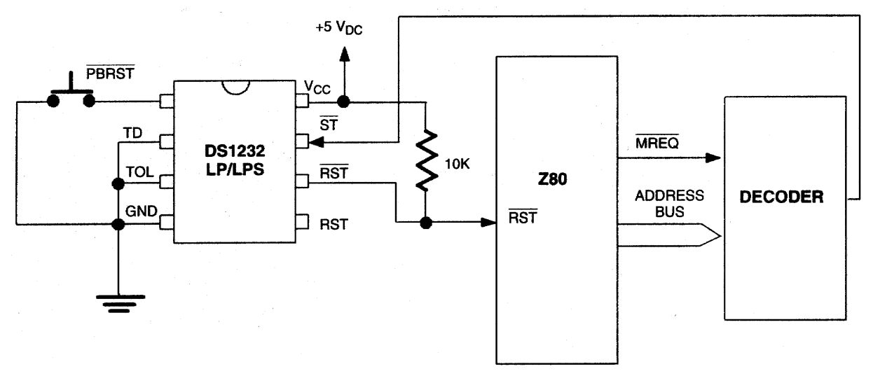
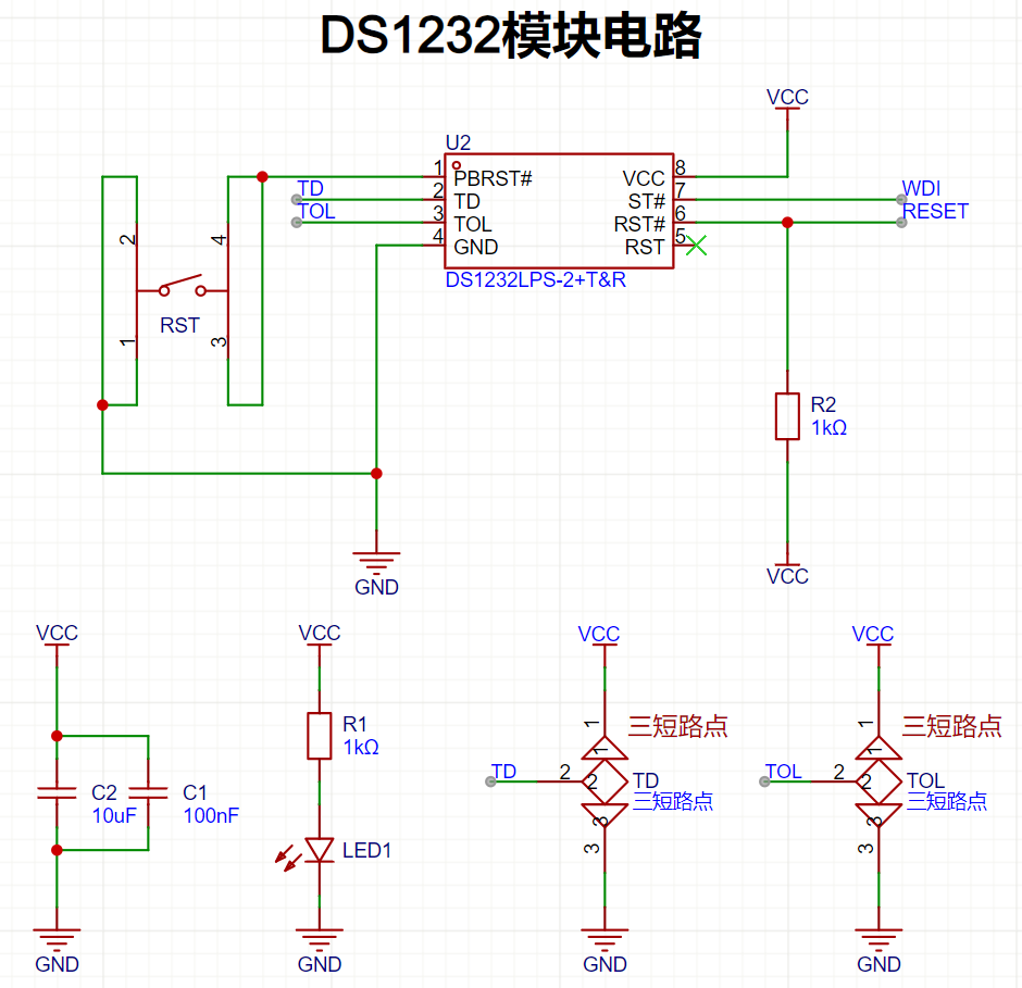
Above diagram shows peripheral application circuit for DS1232. It monitors VCC undervoltage and generates reset signals(RST active‑high, /RST active‑low) on fault, together with built‑in watchdog function.
- MCU must generate high‑to‑low feed‑dog pulse on ST pin within timeout window defined by TD pin; otherwise the module outputs reset for minimum 250 ms. PBRST is external push‑button reset input which forces reset when pressed.
- C1/C2 are power‑supply decoupling capacitors. R1+LED indicates power presence. R2 is pull‑up resistor for open‑drain /RST output. TD and TOL pins use solder‑jumpers or dip‑switches to select watchdog timeout and voltage‑threshold settings.
Note DS1232 is designed for 5 V systems. If your MCU uses 3.3 V IO levels, implement level‑translation circuitry or select 3.3 V monitor chip to avoid damaging the MCU.
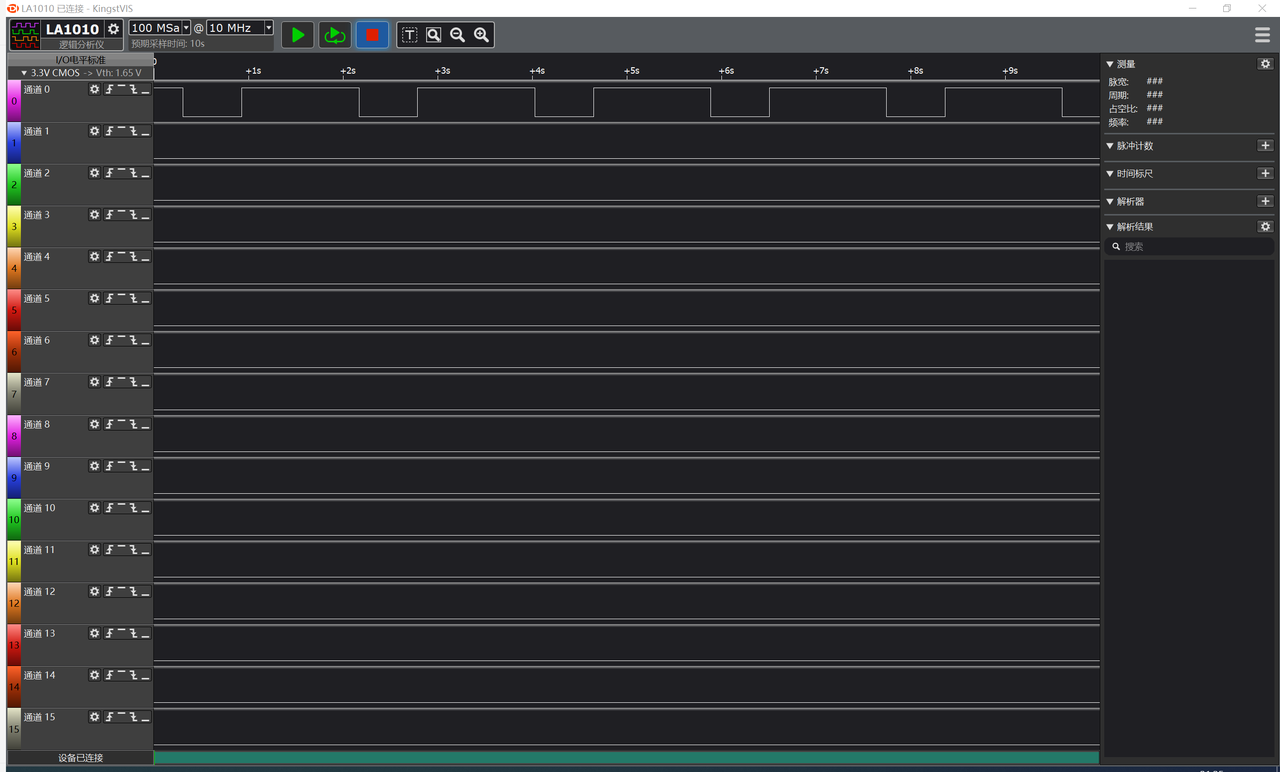
Below are module test results. After power‑on, logic‑analyzer channel 0 is connected to the RST pin of watchdog module.
When TD is tied to VCC: pulse interval must not exceed 1.2 seconds; 2 Hz square‑wave input is recommended:
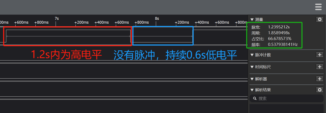
When TD is left floating: pulse interval must not exceed 600 ms; 10 Hz square‑wave input is recommended:
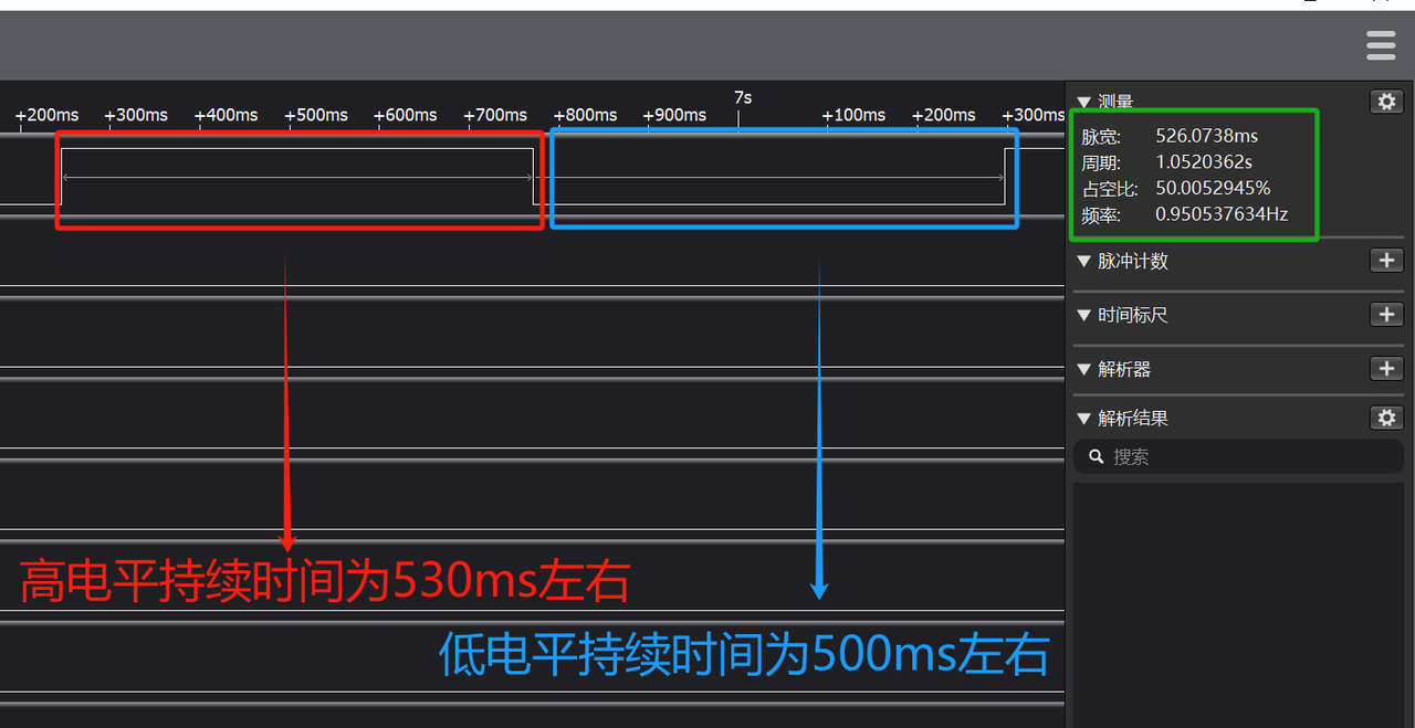
When TD is tied to GND: pulse interval must not exceed 0.15 seconds; 30 Hz square‑wave input is recommended:
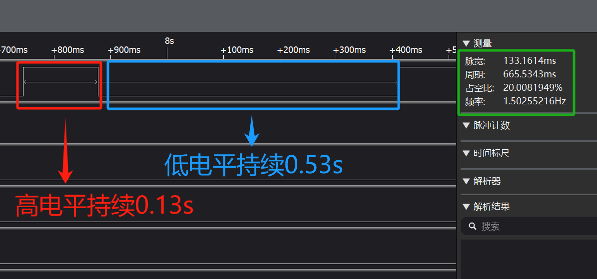
In practical engineering, feed‑dog frequency should be faster than theoretical datasheet limit. This is caused by DS1232 internal timing accuracy error, sampling delay and pulse‑width constraints. Feeding exactly at theoretical maximum timeout often leads to unexpected reset. Engineering practice suggests setting feed‑dog period to one‑half or less of nominal timeout value.
Datasheet shows timing accuracy error is approximately −58.33% / +66.67% relative to typical value:
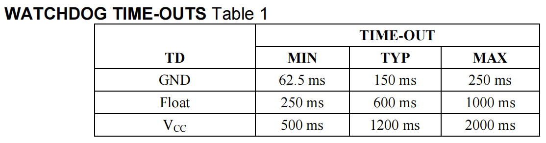
GND mode: typical 150 ms, minimum 62.5 ms (−58.33%), maximum 250 ms (+66.67%).
Float mode: typical 600 ms, minimum 250 ms (−58.33%), maximum 1000 ms (+66.67%).
VCC mode: typical 1200 ms, minimum 500 ms (−58.33%), maximum 2000 ms (+66.67%).