Disassembly of the RP2040 Clock Tree: Clock Sources, Generators and Peripheral Clocks
This article explains RP2040’s clock tree system, covering multiple clock sources, frequency configuration, independent gating and power-saving principles.
COMPONENTS
PROJECT DESCRIPTION
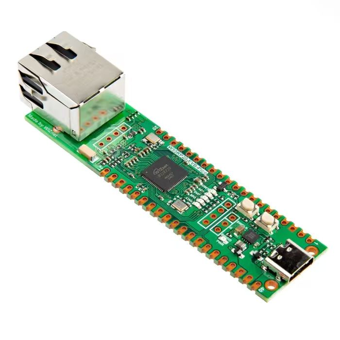
【Preliminary Note】The original hardware example in this article was written based on the RP2040. The actual hardware used in this hands-on demonstration features the W55RP20 as the main controller chip. The circuit logic and UF2 flashing operation principles are universally applicable, with only the main controller model differing. The original chip model mentioned in the circuit descriptions below is provided for reference purposes only.
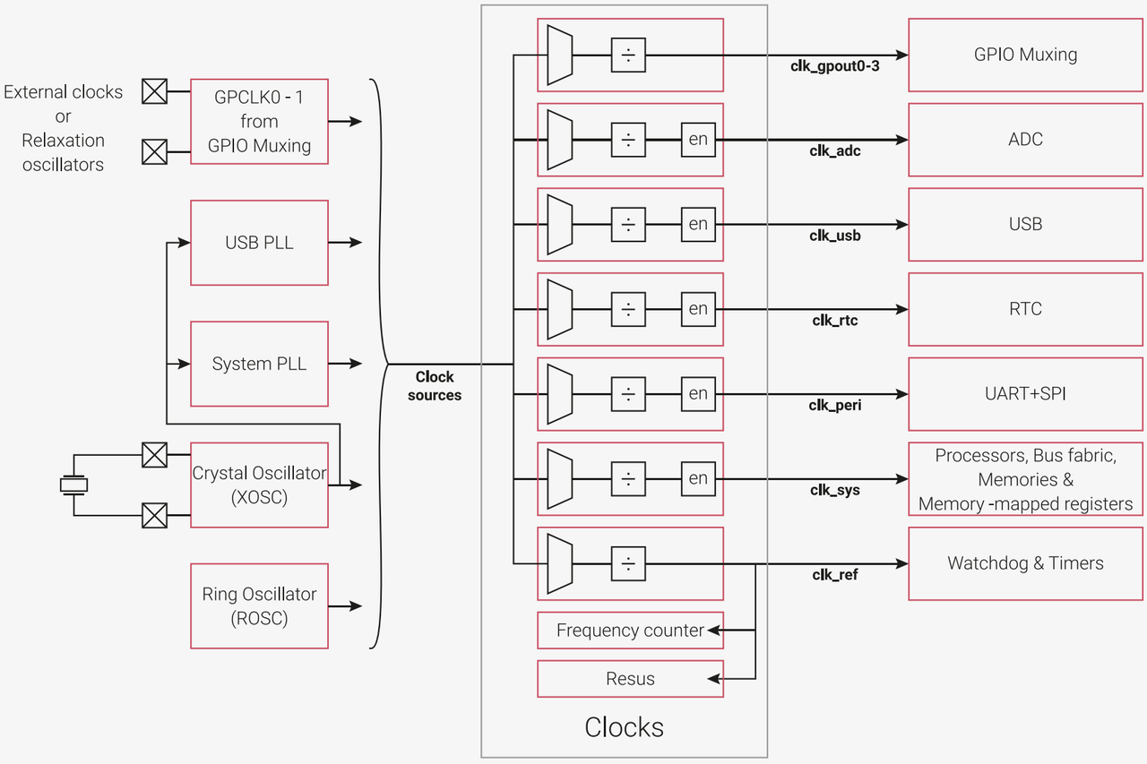
The clock system can introduce clocks from different clock sources (PLL, internal ring oscillator, USB clock, etc.) and use multiple clock generators to provide the required clocks. The clock system can independently start and stop clocks, and change certain clock frequencies while keeping other clock frequencies at their optimal values.
Figure 2.38 Schematic Diagram of Reset Logic Circuit for Chip Subsystem
As can be seen from the above figure:
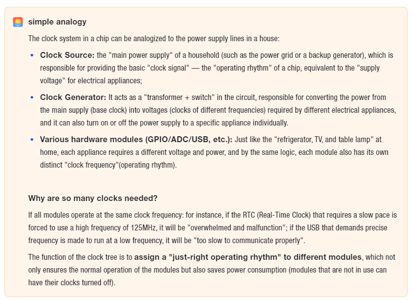
Left side (Clock sources): Clock sources (main power supply): including ring oscillator (ROSC, the built-in "backup small generator" of the chip), crystal oscillator (XOSC, the precise "main power grid"), USB PLL/System PLL (the "voltage amplifier" that boosts the base clock to a high frequency);
Middle (Clocks) Clock Generator (Transformer + Switch): Each generator supports "clock frequency adjustment"(the ÷ sign denotes frequency division, e. g., dividing 125MHz into a lower frequency) and "individual switching"(en stands for enable/switch control);
Each hardware module (electrical appliance) on the right is powered by its corresponding clock generator; for example, USB uses a fixed 48MHz clock, while the system core uses a high-frequency 125MHz clock.
To sum up, the clock system of the RP2040 is essentially a "clock tree": it first obtains the base clock from sources including ring oscillators, crystal oscillators, and PLLs clock sources, then uses multiple clock generators to convert these base clocks into clocks of different frequencies, and distributes them to various modules such as GPIO, ADC, and USB. It also supports independently starting/stopping the clock of a specific module and adjusting the frequency, which not only meets the timing requirements of different modules but also reduces power consumption.
Some common clock parameters are as follows:
PLL_SYS = 125MHz (default), 133MHz (maximum)
PLL_USB = 48MHz (fixed)
CLK_SYS = PLL_SYS / CLK_REF (system clock; selects between these two clocks unless in DORMANT mode)
CLK_PERI = CLK_SYS (peripheral clock)
CLK_USB = PLL_USB (固定)
CLK_ADC = PLL_USB (固定)
CLK_RTC = 46875Hz (for RTC counting, 12MHz / 256 = 46875Hz; when CLKDIV_M1 = 46874, the frequency is 1Hz)