



Dig Into Raspberry‑Pi Pico Memory Internals: Complete Breakdown of ROM, SRAM and Flash
In‑depth introduction to RP2040 underlying memory architecture including ROM, multi‑bank SRAM, XIP external Flash and address‑mapping mechanism
Here we supplement several core "mapping" concepts, which are the foundation of memory access. Afterwards we explain memory‑mapping tables for memory and SRAM. On‑chip resources (memory, registers, peripherals) must be assigned "house numbers" to become accessible. This is the essence of mapping.
Address mapping Assign unique numeric "house numbers" (system addresses) to all on‑chip resources. For example SRAM starts at address 0x20000000, ROM starts at 0x00000000. Cores or DMA use these addresses to locate target resources precisely, acting as a lookup table between resources and their assigned addresses.
Register mapping A subset of address mapping. Assign house numbers to on‑chip registers (small memory locations holding configuration and status). For instance 0x40008000 corresponds to the UART baud‑rate register. Software writes to this address to configure UART hardware. It serves as lookup table for register‑function‑to‑address relationships.
Remapping Re‑assign house numbers. Example: originally address A points to memory; after remapping, address A can point to a peripheral instead. This flexibly adjusts resource‑access addresses for different application scenarios.
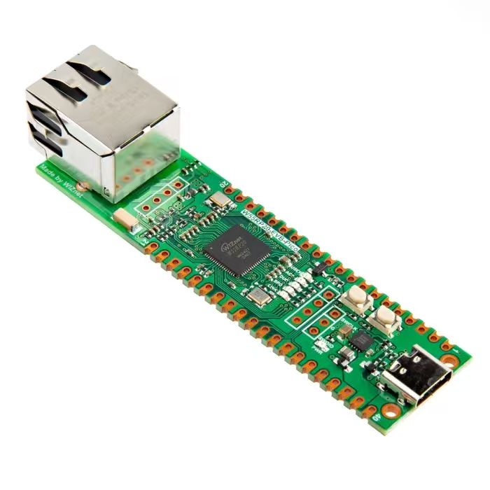
All memory access operations rely on address mapping. The Raspberry‑Pi Pico memory layout consists of 16 kB fixed‑content ROM and 264 kB parallel‑access SRAM. SRAM uses multiple physical memory banks for higher access throughput. An external 2 MB Flash chip is accessed via the QSPI interface.
- ROM
16 kB read‑only ROM at address 0x00000000. ROM content is fixed after chip manufacturing. It contains:
- Initial boot‑loader routines
- Flash boot‑up sequences
- Flash programming routines
- USB mass‑storage device supporting UF2
- Utility libraries such as fast floating‑point math
The ROM bootloader source code can be downloaded at: https://github.com/raspberrypi/pico‑bootrom
This ROM delivers single‑cycle read‑only bus access behind a dedicated AHB‑Lite arbiter, so it may be accessed concurrently alongside other memory peripherals. Write operations targeting ROM produce no effect and do not trigger bus faults.
- SRAM
Total on‑chip SRAM size is 264 kB. Physically it is split into six independent banks. This architecture greatly improves memory bandwidth for multiple bus masters (Core0, Core1, DMA can access different banks simultaneously to avoid resource contention). From the software perspective it appears as one contiguous 264 kB address range for read‑write operations, while physical‑bank routing is handled by hardware address‑mapping.
There are no restrictions on content stored inside each bank; application code, data buffers and other objects can reside in any bank.
Bank composition: four 16k×32‑bit banks (64 kB each) plus two 1k×32‑bit banks (4 kB each).
Every SRAM bank has its own dedicated AHB‑Lite arbiter. Multiple bus masters can access distinct SRAM banks in parallel. Up to four 32‑bit SRAM accesses may complete within one system clock cycle (one access per master).
In memory map, SRAM base address is 0x20000000. Base addresses for each physical bank are shown below.
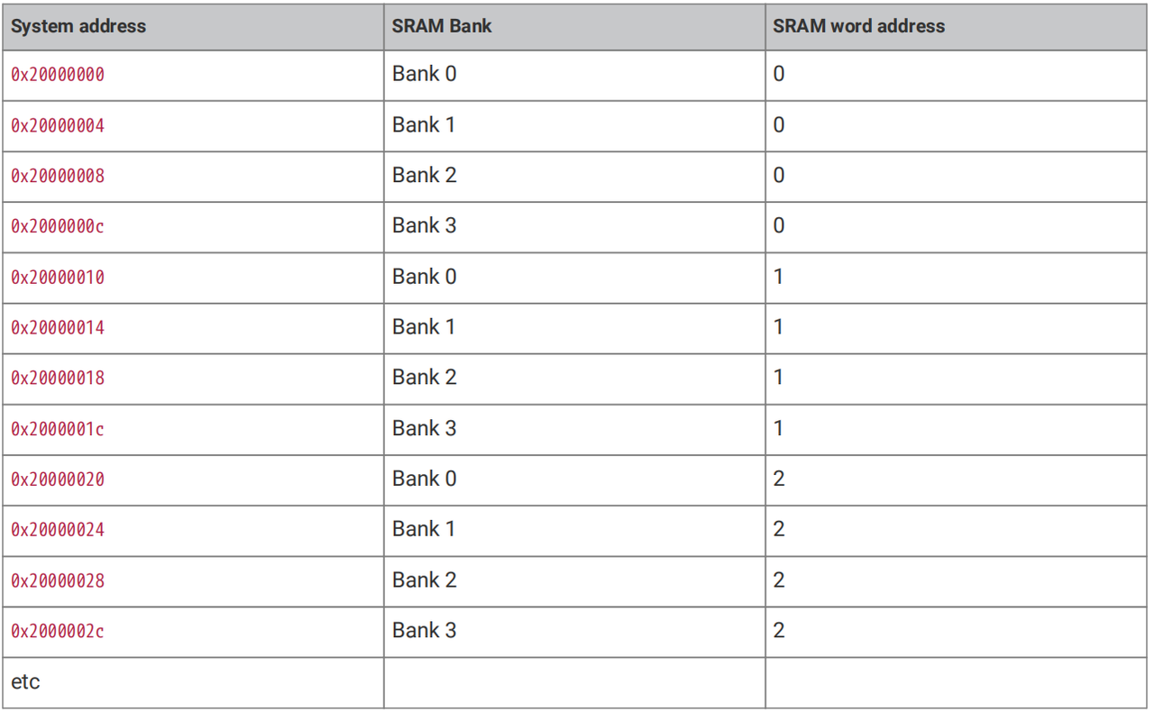
The mapping table includes these fields:
System address The "house number" for SRAM. Cores and DMA use this address to access SRAM. 0x20000000 is the first valid SRAM address.
SRAM Bank Physical SRAM storage block. The table shows Bank0‑Bank3; two extra small 4 kB banks also exist.
SRAM word address "Word" means 32‑bit (4‑byte) unit. This value represents offset index inside the selected physical bank. For example word‑address 0 means first 32‑bit entry inside that bank.
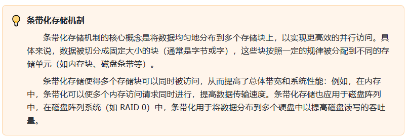
RP2040 SRAM uses striped memory mapping to boost parallel‑access performance. Consecutive system word‑addresses are distributed across the four main banks. Each increment of 4 bytes (one 32‑bit word) cycles through Bank0 → Bank1 → Bank2 → Bank3, then loops back to Bank0 while incrementing the internal word offset.
Example mapping:
0x20000000→ Bank0, word‑address 00x20000004(+4) → Bank1, word‑address 00x20000008(+4) → Bank2, word‑address 00x2000000C(+4) → Bank3, word‑address 00x20000010(+4) → Back to Bank0, word‑address 1
This striped layout enables parallel access: for instance Core0 reads 0x20000000 (Bank0) while DMA reads 0x20000004 (Bank1). The two operations run without interference, significantly improving SRAM read‑write throughput.
Since contiguous byte‑oriented system addresses spread across different physical banks, multiple memory transactions can execute concurrently. This raises overall memory bandwidth and reduces conflicts between memory requests.
Two extra 4 kB regions at 0x20040000 and 0x20041000 map directly onto the two small physical 4 kB SRAM banks. These are commonly reserved for per‑core resources such as stack or frequently‑executed code, helping avoid processor‑stall conditions when accessing these memory ranges.
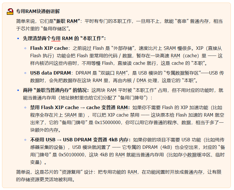
Besides main on‑chip SRAM, two additional RAM blocks can be used under certain conditions:
Flash XIP cache When XIP cache is disabled, this block acts as 16 kB general‑purpose RAM starting at address 0x15000000.
USB DPRAM If the USB peripheral is unused, this 4 kB memory block may serve as ordinary RAM starting at address 0x50100000.
- External Flash
Two key definitions:
QSPI interface High‑speed data bus between MCU chip and external Flash, faster than ordinary SPI. Handles communication with off‑chip Flash memory.
XIP (Execute In Place) "Execute code in‑place". Program code stored inside external Flash does not need to be copied into on‑chip SRAM before running. Code executes directly from external Flash, treating Flash as extended memory and saving SRAM capacity.
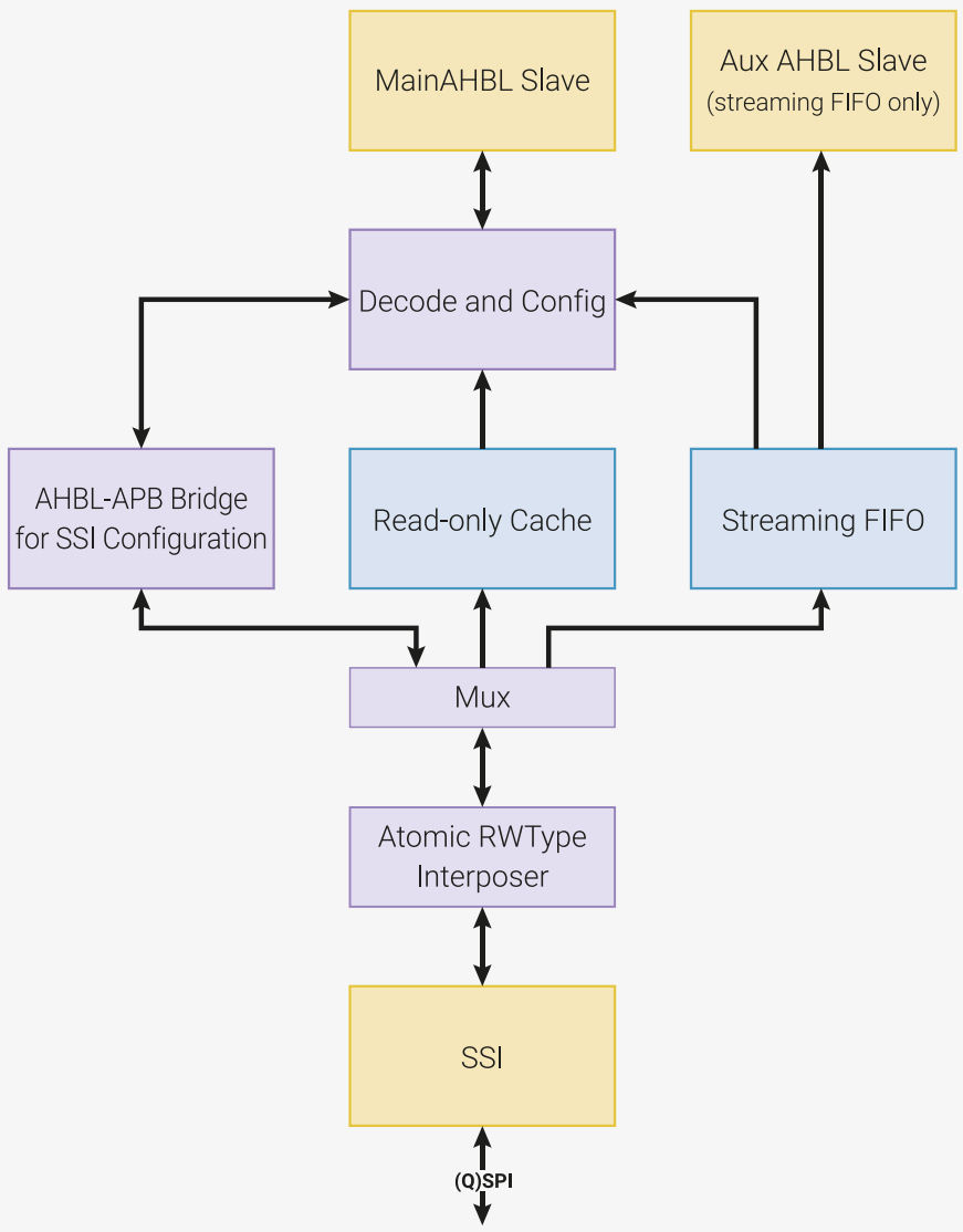
RP2040 Flash management relies on Execute‑In‑Place (XIP) hardware. Four major components enable efficient Flash access: QSPI interface, XIP hardware logic, XIP cache, and SSI serial flash interface.
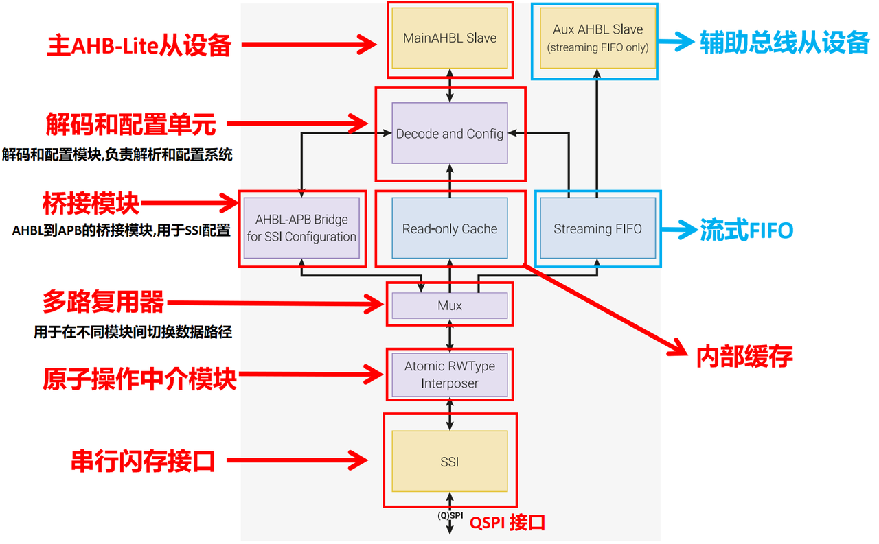
Core design goal: make external Flash behave similarly to on‑chip memory, accelerated by cache while guaranteeing reliable communication.
SSI module Directly connected to QSPI interface; physical‑layer peripheral sending and receiving QSPI signals. It performs raw data transfer with external Flash chips.
Atomic RWType Interposer Guarantees atomic, non‑interrupted Flash read‑write operations. For example a 32‑bit read will not be partially overwritten or interrupted by other transactions to avoid data corruption.
Mux multiplexer Data‑path switch selecting whether data comes from cache or directly from Flash. Cache path is prioritized for better performance.
Read‑only Cache External Flash runs slower than on‑chip SRAM. Cache holds frequently‑used instructions and data fetched from Flash. On access, hardware checks cache first. Cache hits avoid slow Flash access and greatly speed‑up XIP execution.
Streaming FIFO continuous‑data buffer When reading large contiguous blocks from Flash (large program segments, binary files), incoming data is buffered inside this FIFO before delivering to CPU. This prevents choppy data delivery for bulk sequential accesses.
Decode and Config address‑decoding & configuration unit
- Decode incoming system addresses and map them to corresponding locations on external Flash.
- Manage global XIP‑hardware configuration: enable / disable cache, configure QSPI communication bit‑rate, adjust FIFO parameters etc.
Main AHBL Slave / Aux AHBL Slave Bus‑interface ports connecting XIP subsystem onto the AHB‑Lite system bus.
- Main slave: handles regular Flash accesses such as scattered instruction and data fetches.
- Aux slave: dedicated for high‑throughput Streaming‑FIFO continuous‑data transfers.
AHBL‑APB Bridge for SSI Configuration interface for SSI module. CPU configures SSI parameters (QSPI clock frequency, transfer modes) over APB bus to match various external Flash chips.
External Flash (maximum supported size 16 MB) is accessed through QSPI using XIP hardware. The system can address external Flash just like internal memory without pre‑copying code into on‑chip RAM. Accesses targeting the 16 MB memory range starting at address 0x10000000 are translated into read transactions directed to external serial Flash, and results are returned to the originating bus master.
XIP subsystem workflow:
- System access decoding Memory transactions arrive via main AHB‑Lite slave port. Hardware decodes each access: classify it as XIP‑Flash access, direct SSI peripheral configuration access, or access targeting internal XIP control registers.
- XIP access processing
- Cache lookup: For XIP‑type access, hardware first searches inside cache for requested data. On cache‑hit, data is returned directly from cache.
- Cache miss: If requested content is absent from cache, hardware issues serial read request via SSI interface to fetch data from external Flash.
- Data storage and forwarding
- Data storage: Data retrieved from external Flash populates cache for faster future reuse.
- Data forwarding: Retrieved data is forwarded onto system bus to satisfy the original memory request. XIP ensures valid data reaches bus master and processor.
3.1 XIP Cache Mechanism
XIP cache is 16 kB two‑way set‑associates internal buffer to accelerate external‑Flash access. Cache hit latency is one system clock cycle. This cache serves exclusively for XIP‑Flash access. Software normally does not need to manage cache coherency, except after Flash reprogramming operations.
Cache maps onto 24‑bit Flash address space. RP2040 system‑address upper 8‑bits perform segment decoding; lower 24‑bits map to Flash offset, supporting maximum 16 MB Flash. Multiple mirrored address ranges in RP2040 address space implement different cache behaviours:
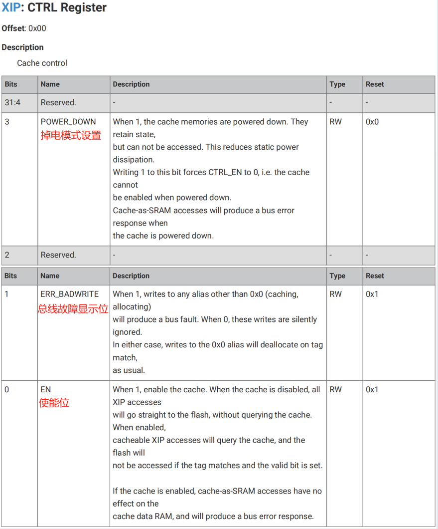
0x10… : XIP access, cacheable‑allocating. Normal caching behaviour; cache fills with new data on cache‑miss. 0x11… : XIP access, cacheable‑non‑allocating. Check for cache‑hit, but do not populate cache on miss. 0x12… : XIP access, non‑cacheable‑allocating. Skip cache lookup; always read Flash, but fill cache with returned data. 0x13… : XIP access, non‑cacheable‑non‑allocating. Fully bypass cache; read directly from Flash. 0x15… : XIP‑cache‑as‑SRAM mirror range. When cache hardware is disabled (clear CTRL.EN bit), this region behaves as an extra 16 kB SRAM. Reads‑writes complete in one cycle; write‑then‑read sequences introduce one wait‑state.
When CTRL.EN bit clears to disable cache, all 0x10‑0x13 XIP mirrors bypass cache and directly hit Flash, noticeably degrading XIP code‑execution speed.
3.2 XIP Cache Flush and Maintenance
After software reprograms Flash content, stale old data still residing inside cache must be invalidated to guarantee correct runtime behaviour without full system reboot. The FLUSH register is used to purge entire cache contents.
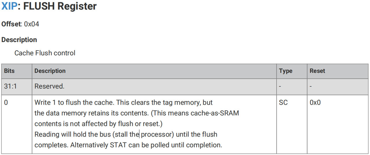
Write logic‑1 to bit 0 of FLUSH register to trigger full cache flush. Flush works by zeroing tag‑memory entries. For 16 kB cache with 8‑byte lines and two‑way associativity, flush consumes roughly 1024 clock cycles.
Reading bit 0 of FLUSH register blocks CPU until flush completes. Polling the STAT register is another method to monitor flush progress.
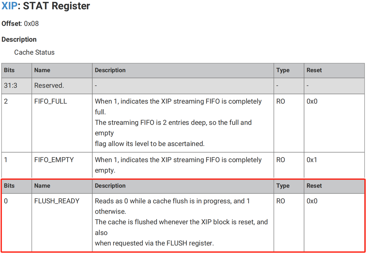
Flash access remains safe during ongoing cache flush: other bus‑masters attempting Flash access stall until flush finishes to prevent inconsistent data reads.
Warning: When cache hardware is disabled and used as SRAM via 0x15… mirror, flush command will not modify this SRAM content. But issuing writes to this SRAM region concurrently with cache flush may corrupt data. To avoid corruption, ensure flush operation fully completes before issuing writes to this SRAM alias.
Full‑cache flush significantly lowers performance afterwards until cache warms‑up again. As alternative, selectively invalidate only affected cache lines. After erasing‑reprogramming one Flash sector, you only need to invalidate corresponding cache entries rather than full flush. On RP2040, writing to addresses inside 0x10… mirror triggers selective invalidation:
- Look‑up cache entries matching target address range.
- Mark matched cache entries as invalid. Next access reloads fresh content from Flash.
3.3 SSI Serial Flash Interface
SSI (Synchronous Serial Interface) is RP2040 peripheral dedicated to serial Flash transactions. It supports standard SPI, dual‑SPI (DSPI), quad‑SPI (QSPI). Multiple operation modes enable XIP execution with nearly all serial‑Flash chips.
Maximum SSI SPI clock is half of system clock frequency. It supports inserting instruction prefix or mode‑continuation bits for each XIP access. It also implements standard SPI‑host FIFO mode with built‑in DMA support for high‑speed bulk transfers.
3.4 Flash Streaming and Auxiliary Bus Slave
Flash capacity is generally far larger than on‑chip SRAM. Bulk data transfers from Flash into RAM benefit from streaming mechanism. DMA performs streaming data movement in background while CPU executes other foreground tasks.
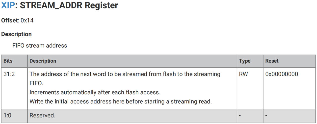
Normal XIP execution interacts poorly with streaming. SSI serial transfers introduce long bus‑latency for DMA. While CPU often tolerates this (high cache‑hit ratio during code fetch), long stalls starve other active DMA channels and degrade overall DMA throughput. RP2040 solves this problem with streaming hardware controlled by STREAM_ADDR and STREAM_CTR registers for efficient bulk Flash‑to‑SRAM loading.
STREAM_ADDR register sets starting Flash address for streaming read.
STREAM_CTR register starts‑stops streaming operation.
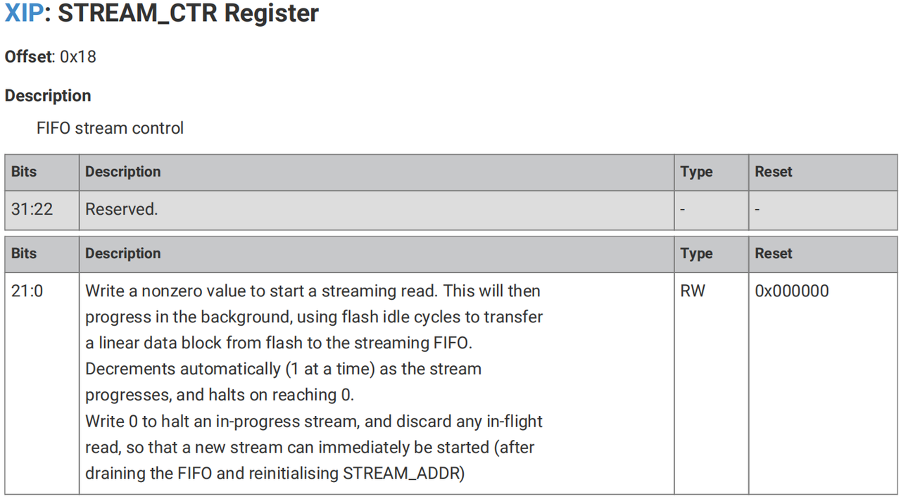
Operation description: Write non‑zero value: start background streaming. Hardware reads linear block from Flash during Flash idle cycles and fills streaming FIFO. Counter auto‑decrements on each transfer; streaming auto‑stops once counter reaches zero. Write zero value: abort ongoing streaming and discard pending FIFO data.
After configuration, XIP subsystem handles background read operations without CPU polling. Streaming hardware runs at lower priority, so it will not heavily interfere with CPU execution.
After cache‑miss events, streaming hardware inserts a short seven‑clock cooling interval to avoid adding extra latency for regular XIP traffic.
Data read from Flash fills streaming FIFO buffer. Once data is available inside FIFO, hardware asserts DREQ signal to notify DMA controller. DMA fetches data out of FIFO and moves it to target memory or peripheral. DMA only reads FIFO on valid DREQ and will not stall waiting for slow Flash reads.
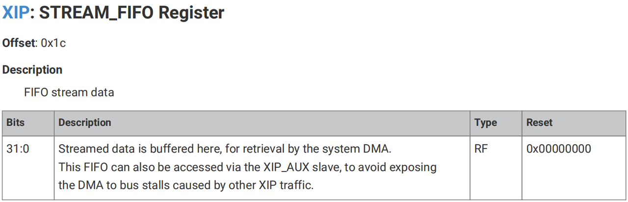
Even when FIFO holds valid data, DMA may stall if other bus‑masters are accessing XIP Flash and trigger cache‑miss delays. RP2040 introduces auxiliary bus‑slave dedicated exclusively for streaming‑FIFO access. This slave connects to FASTPERI arbiter serving zero‑wait‑state native AHB‑Lite peripherals. DMA accesses to streaming FIFO via auxiliary slave are isolated and unaffected by other Flash‑related bus‑stalls.
3.5 Performance Counters
RP2040 XIP subsystem includes two 32‑bit performance counters for cache‑efficiency profiling, helping developers optimize code layout. Counters wrap to zero after hitting maximum value 0xFFFFFFFF. Writing any value resets each counter.
Counter 1 — Total XIP accesses: increments for every XIP‑Flash access regardless of cache‑hit or miss.
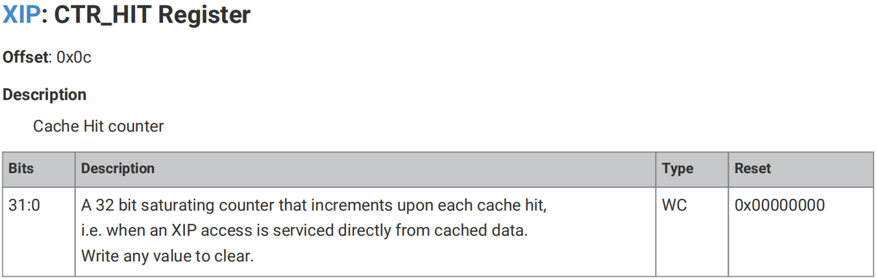
Counter 2 — XIP cache hits: increments when requested data is already present inside cache.
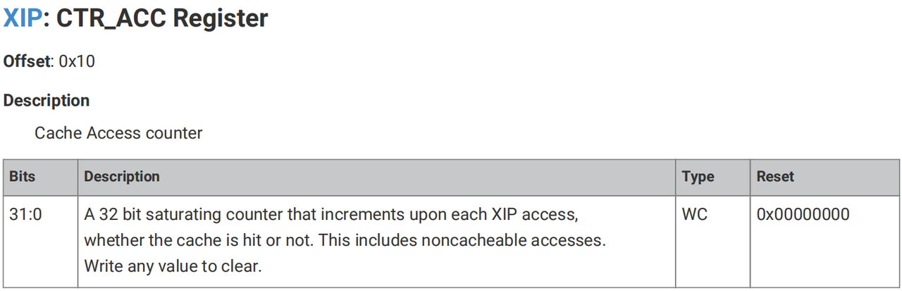
Combining these two counters allows calculation of cache‑hit ratio for evaluating cache‑utilization efficiency and identifying optimization opportunities.