Deep Dive into Raspberry‑Pi Pico DMA: Registers to Chained Transfers
RP2040 DMA low‑level analysis covering registers, triggers, chaining and practical points
- DMA Unit on Raspberry‑Pi Pico
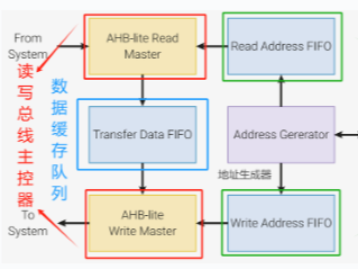
The RP2040 DMA controller features independent read‑master and write‑master interfaces connected to the chip bus fabric, enabling parallel read and write DMA operations. Key architectural characteristics:
Read master: can read data from an address every clock cycle. Write master: can write data to another address every clock cycle. This means DMA can perform one read access and one write access simultaneously within a single clock cycle, transferring up to 32‑bits of data per cycle.
Address generator The address generator produces matching read‑address and write‑address values and feeds them to read‑master / write‑master via address FIFO. The FIFO acts as a critical buffer inside the DMA architecture to guarantee smooth data flow.
Independent channels RP2040 DMA controller provides 12 independent DMA channels. Each channel manages its own sequence of bus transfers. Multiple transfer sequences can run concurrently. Every channel has dedicated Control‑and‑Status Registers (CSRs) for software configuration and status monitoring.
Multi‑channel concurrency When several channels are active at the same time, DMA uses round‑robin scheduling to fairly allocate bus bandwidth among requesting channels for balanced resource usage.
RP2040 DMA supports three transfer directions: memory‑to‑peripheral, peripheral‑to‑memory, memory‑to‑memory.
Each DMA channel exposes control‑and‑status registers for software configuration of the following parameters:
Transfer direction Configure data flow direction: memory‑to‑peripheral, peripheral‑to‑memory or memory‑to‑memory.
Transfer data size Supported transfer widths: 32‑bit, 16‑bit, 8‑bit. Source and destination data width for a given channel must be identical.
Address update DMA automatically increments or decrements source and destination pointers according to configuration to stream sequential data from source to destination.
Transfer mode Supports single‑shot transfer and circular transfer modes. Circular mode allows continuous repeated transfers without re‑programming registers.
Chaining One DMA channel can trigger another channel to execute subsequent work via the CHAIN_TO bit. This callback‑style cooperation lets the DMA controller execute complex workflows autonomously.
CHAIN_TO bit field resides inside the DMA channel trigger‑control register
- DMA Channel Configuration
Each DMA channel has four primary Control‑and‑Status Registers (CSRs) governing data transfers:
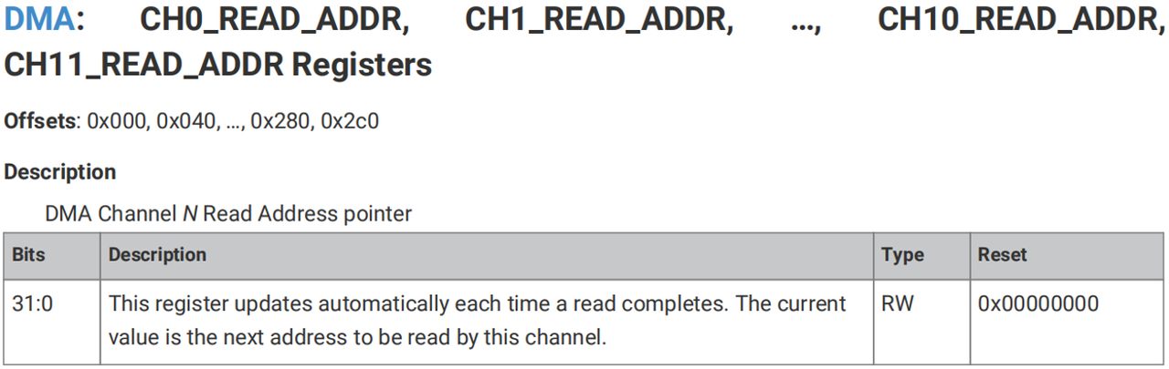
READ_ADDR (Read‑Address Register) Pointer for read operations. This register auto‑updates to the next read address after each completed read transaction.
WRITE_ADDR (Write‑Address Register) Pointer for write operations. Auto‑updates to next destination address after each completed write transaction.
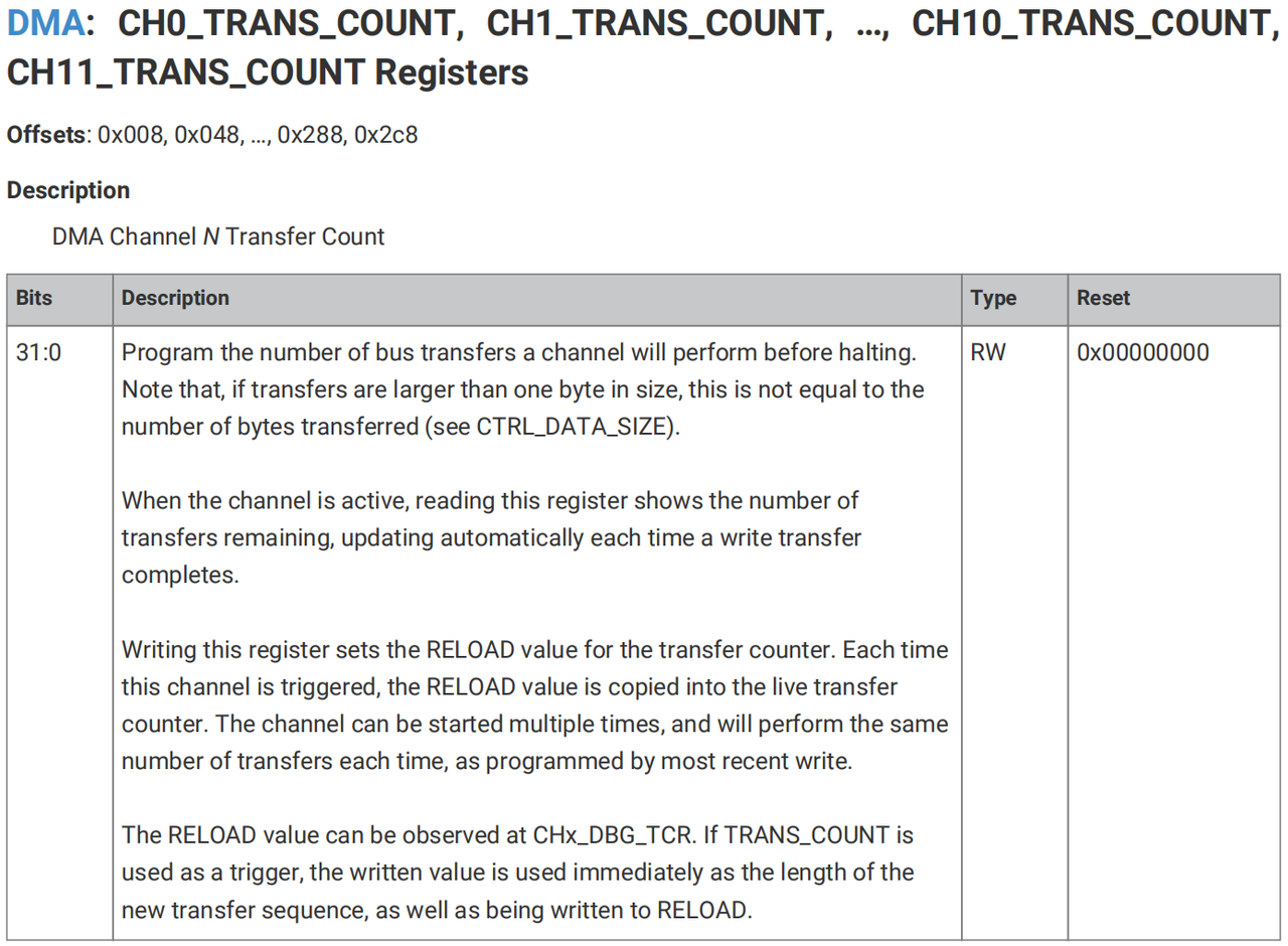
TRANS_COUNT (Transfer‑Count Register) Sets total number of transfers for one sequence (each transfer may be 1‑byte, 2‑byte or 4‑byte). While transfer is in progress, reading this register returns remaining transfer count, which decrements automatically after every write completion.
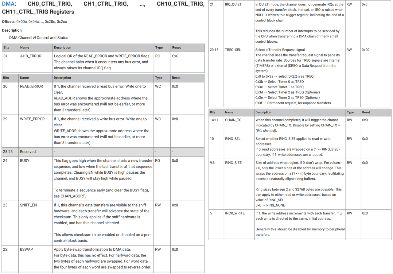
CTRL (Control‑and‑Trigger Register) Manages channel enable, configuration and status monitoring. Key bit‑fields include EN enable bit, BUSY busy flag, TREQ_SEL transfer‑request selector, CHAIN_TO chaining trigger, DATA_SIZE transfer‑width setting, RING_SIZE address‑wrap configuration, plus error indicators and priority bits.
2.1 Read‑Address and Write‑Address Registers
READ_ADDR and WRITE_ADDR store memory pointers for next read and next‑write access. They auto‑advance after each transaction with step size determined by CTRL.DATA_SIZE.
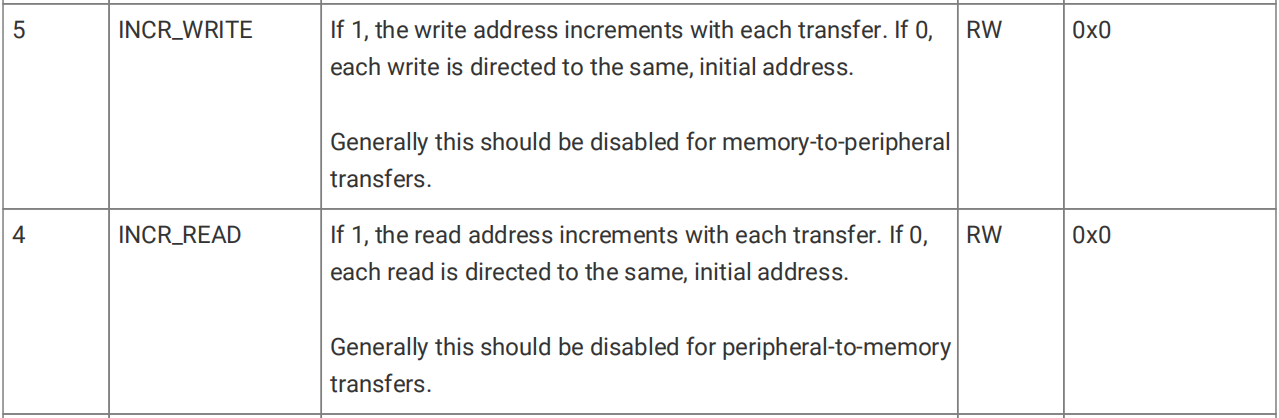
Auto‑increment for read / write pointers can be turned on or off via CTRL.INCR_WRITE and CTRL.INCR_READ. Increment step equals transfer width: 1‑byte, 2‑byte or 4‑byte.
Important note: READ_ADDR and WRITE_ADDR must always be aligned according to CTRL.DATA_SIZE. Byte transfers require 1‑byte alignment; half‑word (16‑bit) transfers require 2‑byte alignment; word (32‑bit) transfers require 4‑byte alignment.
Transfer width is configured by CTRL.DATA_SIZE.
Normally software reloads these registers with new start addresses before starting each new transfer sequence. Two use‑cases skip pointer increment:
Fixed‑peripheral‑FIFO access When accessing a peripheral FIFO register, read/write always targets the same physical address; no pointer advance is needed between consecutive sequences.
Contiguous multi‑block memory transfers DMA can jump automatically from end of one buffer to start of next buffer without software intervention when moving multiple predefined memory blocks. Existing register values become starting pointers for subsequent transfers.
2.2 Transfer‑Count Register
TRANS_COUNT manages remaining transfer operations inside active sequence and defines total transfer count for upcoming sequence:
Reading TRANS_COUNT During ongoing transfer, returns remaining number of transfers; value decrements automatically as work proceeds.
Writing TRANS_COUNT Write value defines total transfers for next sequence. Upon channel activation, written value is loaded into working counter and decrements for each completed transaction.
Transfer‑count reload mechanism The most‑recently written value is copied into live counter on sequence start and counts down until completion. The reload value can be inspected via DBG_TCR debug register.
DBG_TCR debug register exposes reload counter value for inspection.
Automatic repeated transfer count If TRANS_COUNT is not re‑written between successive channel triggers, every trigger uses the same preset transfer count. This is useful for channel chaining: one channel loads control‑block values into CSR registers of another channel; TRANS_COUNT is programmed once and reused on every chained trigger without software reconfiguration.
Custom per‑sequence transfer count Optionally write new value into TRANS_COUNT before every sequence to dynamically change transfer length. When you require variable‑length transfers for each run, write fresh value before starting sequence; channel immediately uses newly‑written count instead of old reload value. If writing to TRANS_COUNT itself acts as channel trigger, new value takes effect immediately.
Note: TRANS_COUNT represents number of transfer operations. Total byte count equals TRANS_COUNT multiplied by per‑transfer width (CTRL.DATA_SIZE):
- DATA_SIZE = 1‑byte → total bytes = TRANS_COUNT
- DATA_SIZE = 2‑byte (half‑word) → total bytes = TRANS_COUNT × 2
- DATA_SIZE = 4‑byte (word) → total bytes = TRANS_COUNT × 4
2.3 Control‑and‑Trigger Register
CTRL register handles comprehensive channel configuration including transfer width, pointer increment rules, chaining, peripheral data‑request selection, status monitoring and fault detection.
- Configure transfer data size (CTRL.DATA_SIZE) Sets per‑transfer width: 1‑byte, 2‑byte or 4‑byte. Read‑side and write‑side transfer widths are identical for one channel.
- Configure address‑increment behaviour
CTRL.INCR_WRITEandCTRL.INCR_READcontrol whether write‑pointer (WRITE_ADDR) and read‑pointer (READ_ADDR) advance after each transaction. Increment step matches DATA‑SIZE setting.CTRL.RING_SELandCTRL.RING_SIZEcontrol circular‑buffer behaviour.
Circular‑buffer mode makes address pointers wrap back to buffer start at predefined boundary, commonly used for peripheral‑FIFO streaming. CTRL.RING_SEL selects whether RING_SIZE applies to read pointer or write pointer. CTRL.RING_SIZE sets circular‑buffer size. Value supplied is exponent for buffer‑size calculation. For example ring_size = 8 means lower 8 address bits wrap → 256‑byte boundary. Valid ring‑size argument is integer between 0 and 31.
- Configure channel chaining (CTRL.CHAIN_TO)

CTRL.CHAIN_TO selects target channel to be triggered when current channel finishes transfer. This mechanism is channel chaining. Multiple DMA channels execute sequentially without CPU intervention, suitable for complex workflows. Assign target‑channel index to CHAIN_TO; target channel fires automatically upon completion of current channel.
- Select peripheral data‑request signal (CTRL.TREQ_SEL)
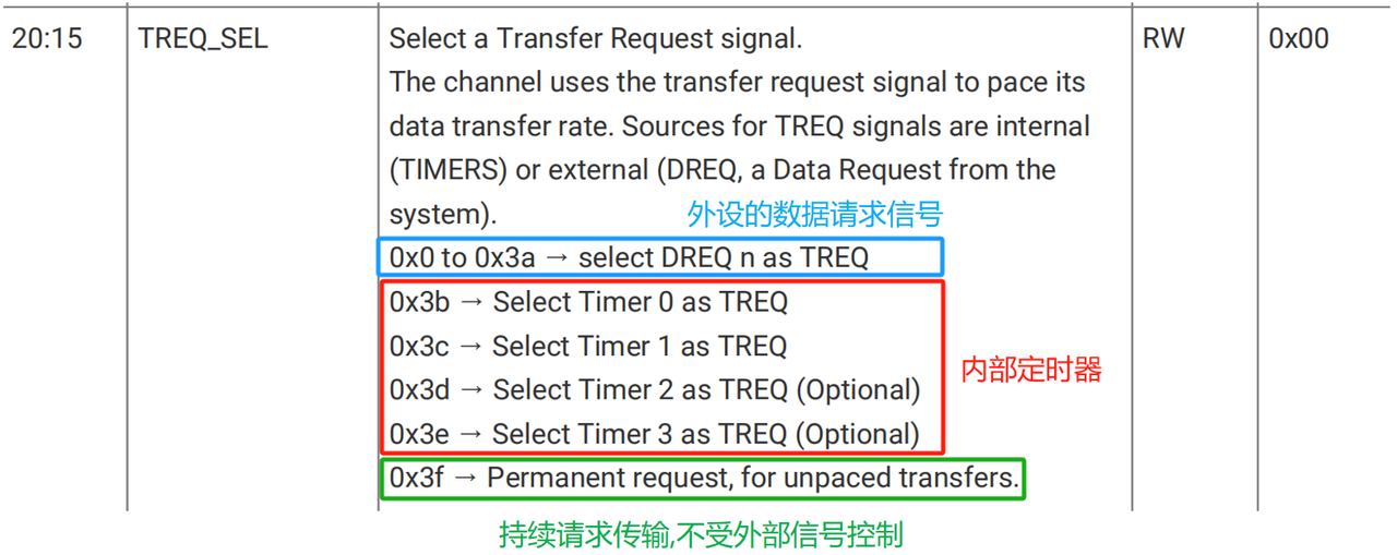
CTRL.TREQ_SEL picks peripheral DREQ (data‑request) signal to pace DMA transfer rate. Peripherals such as UART, SPI, I2C assert DREQ to throttle DMA for hardware‑synchronized streaming. If no peripheral DREQ is selected, DMA runs at full internal clock rate with no external pacing.
- Check channel busy status (CTRL.BUSY)
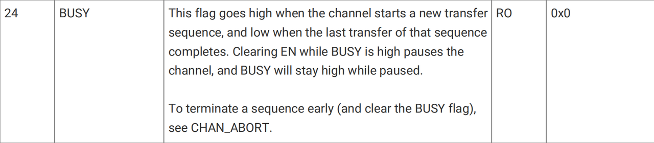
CTRL.BUSY indicates channel activity: Value = 1 → channel is actively transferring data. Value = 0 → channel is idle and accepts new jobs. Software polls BUSY flag to decide submission of new work. Use CHAN_ABORT register to abort ongoing transfer and clear BUSY flag.
- Bus‑error detection (CTRL.AHB_ERROR, CTRL.READ_ERROR, CTRL.WRITE_ERROR) Assertion of any of these bits signals fault during DMA operation for debug and error handling.
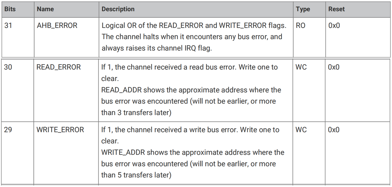
CTRL.AHB_ERROR: AHB bus fault, caused by invalid memory or peripheral‑address access. CTRL.READ_ERROR: Fault occurs during DMA read phase. CTRL.WRITE_ERROR: Fault occurs during DMA write phase.
- Starting DMA Channel Transfers
Three methods exist to launch a DMA channel:
Write to channel control‑trigger register Trigger channel by writing to dedicated control‑trigger register. Simple and efficient, suitable for use inside Interrupt‑Service‑Routines (ISR).

Chained trigger (trigger originating from another DMA channel) If source‑channel CHAIN_TO is configured, completion of source channel automatically fires target channel.
Multi‑channel trigger register (MULTI_CHAN_TRIGGER) Launch multiple DMA channels simultaneously with single register write for parallel‑transfer scenarios.
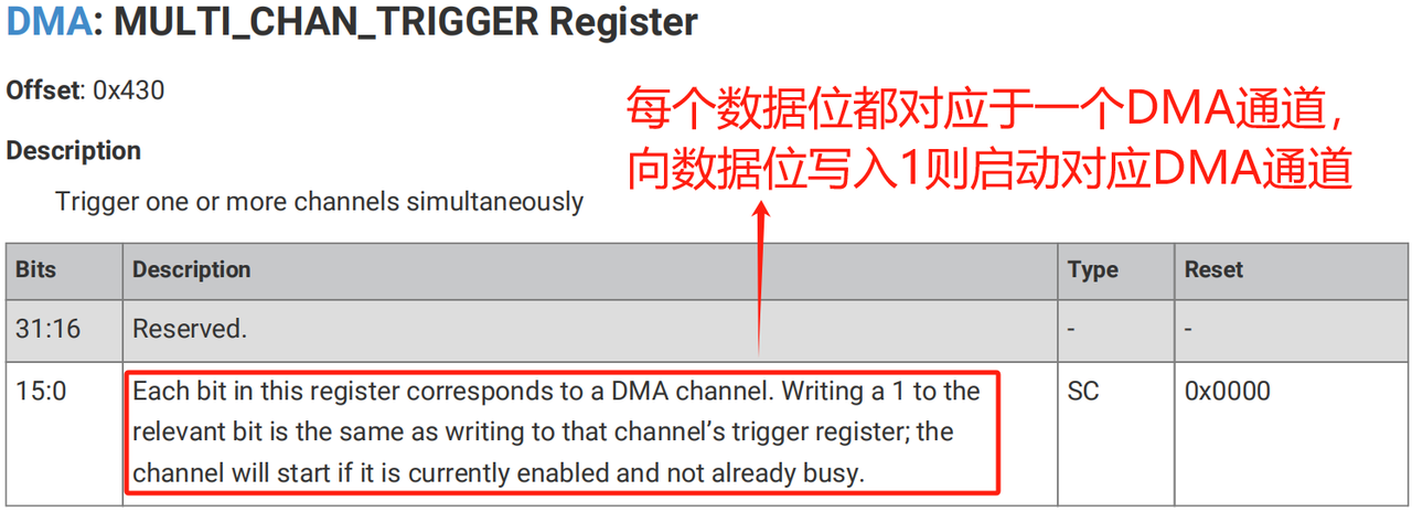
Important: Triggering an already‑active DMA channel has no effect.
3.1 Register Aliases and Trigger Mechanism
Each DMA channel has four main Control‑and‑Status Registers (CSR): READ_ADDR, WRITE_ADDR, TRANS_COUNT, CTRL_TRIG.
These physical registers are exposed via four different alias views in memory. Aliases access identical hardware registers but re‑order register layout.
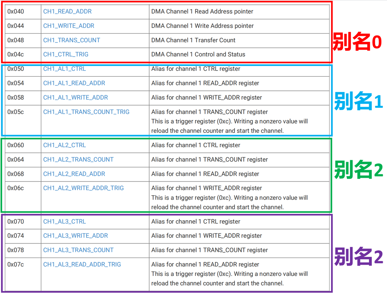
Control‑status registers and four aliases for DMA channel 1.
Address‑offset layout for aliases:
The final register at offset +0xC within each alias block acts as trigger register; writing to it starts DMA channel.
Alias benefit: you can start DMA by writing only critical register without reprogramming full register set.
Memory‑to‑peripheral direction: write READ_ADDR_TRIG alias → configures read pointer and triggers channel in one operation.
Peripheral‑to‑memory direction: write WRITE_ADDR_TRIG alias → configures write pointer and triggers channel in one operation.
For chaining workflows aliases enable compact control‑block lists, only writing registers whose values change:
(WRITE_ADDR, TRANS_COUNT_TRIG): Scatter‑operation, distribute peripheral data into multiple memory buffers. Write destination pointer plus trigger‑count register to launch channel.
(TRANS_COUNT, READ_ADDR_TRIG): Gather‑operation, assemble multiple memory‑block data and push to peripheral. Minimize register‑write overhead.
Situations preventing DMA‑channel start:
Channel disabled: CTRL.EN bit cleared; writes to trigger register produce no action.
Channel already running: trigger is ignored.
Writing value zero to trigger register: channel will not activate.
3.2 DMA Channel Chained Triggering
Chaining allows completion of one DMA channel to immediately start another channel, enabling multi‑channel autonomous cooperation. Typical usecases include re‑configuring peer channels or even re‑arming original channel.
Chaining is configured by CHAIN_TO 4‑bit field inside CTRL register, specifying index of target channel to fire upon completion of current channel.

CHAIN‑TO bit‑field inside CTRL register.
Note: channel cannot chain‑trigger itself. Setting CHAIN‑TO equal to current‑channel index yields no action. Chained trigger behaves identically to other trigger sources and reloads target‑channel transfer counter.
Common practical patterns:
Channel re‑configuration Channel‑A transfers control‑block data into CSR registers of channel‑B. When channel‑B finishes, it chains‑back to restart channel‑A. This executes sequences of jobs autonomously. Control‑blocks store complete DMA‑channel configuration parameters for compact autonomous sequences.
Ping‑pong operation Channel‑A completion triggers channel‑B; channel‑B completion triggers channel‑A. Two channels alternate work forming pipeline‑style execution. CPU can re‑prepare buffers between jobs while pre‑configured chained channels start instantly. Greatly improves throughput for short‑transfer workloads without waiting for CPU intervention.
3.3 Null Trigger and Chain Interrupt
Null Trigger means writing all‑zero value into trigger register. Channel will not start. Two main purposes:
Terminate control‑block sequence Append an all‑zero control‑block entry at end of chain. Null‑trigger stops further channel activations providing autonomous sequence termination.
Reduce interrupt frequency By default every channel‑completion raises interrupt unless masked with INTE0 / INTE1. Long control‑block chains would flood CPU with interrupts. Null‑trigger combined with IRQ_QUIET suppress intermediate interrupts; interrupt occurs only at final null‑trigger.
IRQ_QUIET bit inside CTRL register defaults to 0: interrupt fires on every sequence completion. When set to 1, interrupt is generated only upon receiving null‑trigger.
IRQ_QUIET bit‑field inside CTRL register.
- DMA Data Request
Embedded peripherals such as UART, SPI, ADC produce or consume data at variable rates. RP2040 DMA uses DREQ (Data Request) mechanism to synchronize DMA‑transfer speed with peripheral throughput and avoid data loss / overflow.
DREQ acts as handshake signal between peripheral and DMA: Peripheral asserts DREQ when ready to accept more incoming data. Peripheral de‑asserts DREQ when internal buffer is full or busy; DMA pauses transfers to prevent overflow.
TREQ‑selection bit‑field CTRL.TREQ_SEL configures DREQ source:
External peripheral DREQ Select DREQ signal from target peripheral; DMA transfer pace follows peripheral hardware handshake, e.g. SPI asserts DREQ when ready for next byte.
Internal pacing timer Select DMA‑internal pacing timer. DMA transfers run at fixed software‑defined rate independent of external peripherals; suitable for audio‑stream playback.
No TREQ (disable DREQ) DMA runs at maximum bus speed without external pacing. Mainly used for memory‑to‑memory transfers.
System DREQ mapping table lists all peripheral DREQ channel assignments:
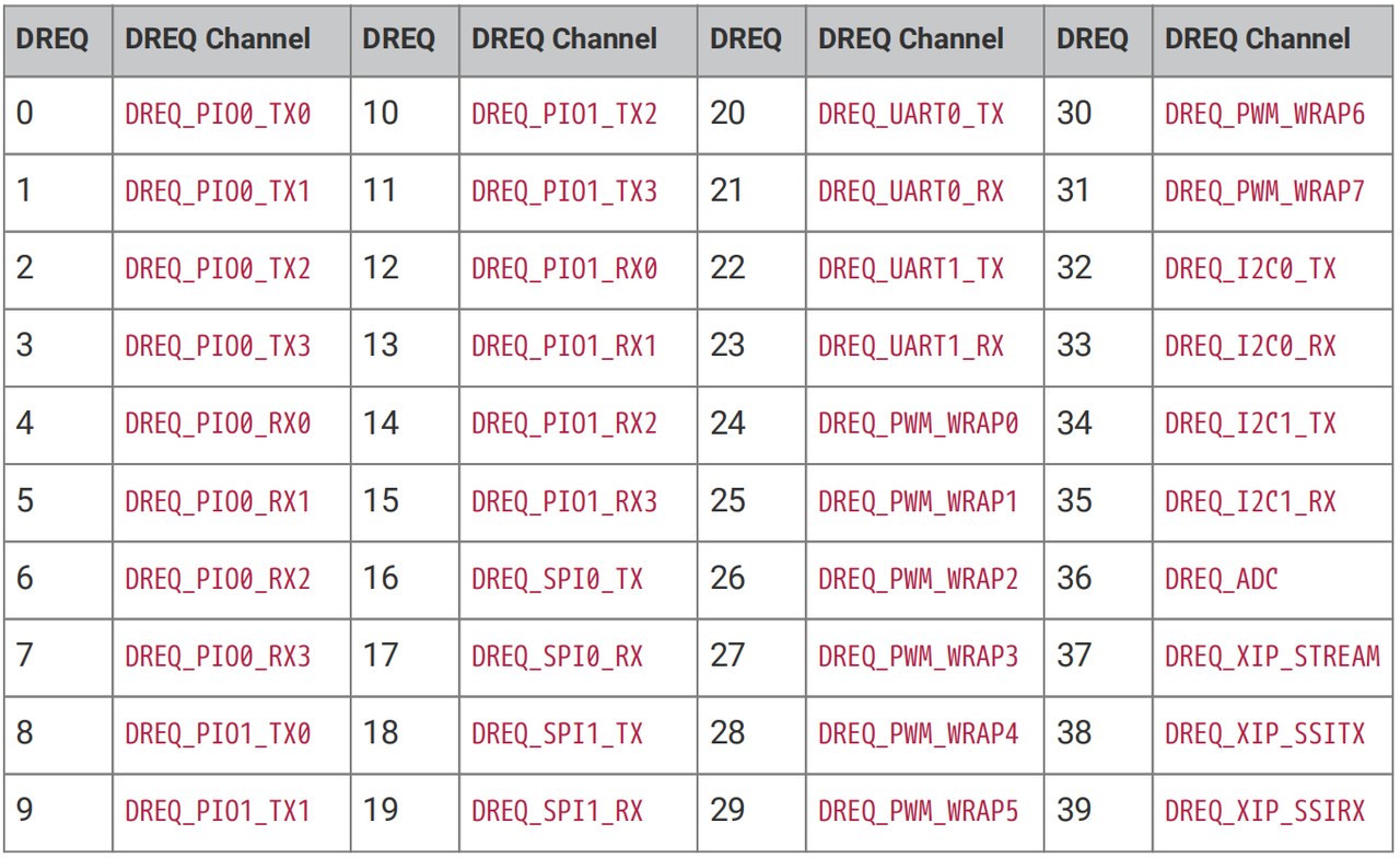
DREQ_PIO0_TX0 ~ DREQ_PIO0_RX3: DREQ for PIO0, TX = transmit direction, RX = receive direction. DREQ_PIO1_TX0 ~ DREQ_PIO1_RX3: DREQ for PIO1. DREQ_UART0_TX, DREQ_UART0_RX: transmit and receive DREQ for UART0. DREQ_UART1_TX, DREQ_UART1_RX: transmit and receive DREQ for UART1. DREQ_SPI0_TX, DREQ_SPI0_RX: transmit and receive DREQ for SPI0. DREQ_SPI1_TX, DREQ_SPI1_RX: transmit and receive DREQ for SPI1. DREQ_PWM_WRAP0 ~ DREQ_PWM_WRAP7: PWM period‑wrap request signals. DREQ_I2C0_TX, DREQ_I2C0_RX: transmit and receive DREQ for I2C0. DREQ_I2C1_TX, DREQ_I2C1_RX: transmit and receive DREQ for I2C1. DREQ_ADC: DREQ associated with ADC peripheral. DREQ_XIP_STREAM, DREQ_XIP_SSITX, DREQ_XIP_SSIRX: DREQ for XIP execute‑in‑place peripheral stream and SPI‑related requests.
- DMA Channel Interrupts
DMA‑channel interrupt request asserts under two conditions:
Completion of transfer sequence: interrupt fires when channel finishes transfer, provided CTRL.IRQ_QUIET = 0.
Receiving null trigger: interrupt fires if CTRL.IRQ_QUIET = 1 upon null‑trigger event.
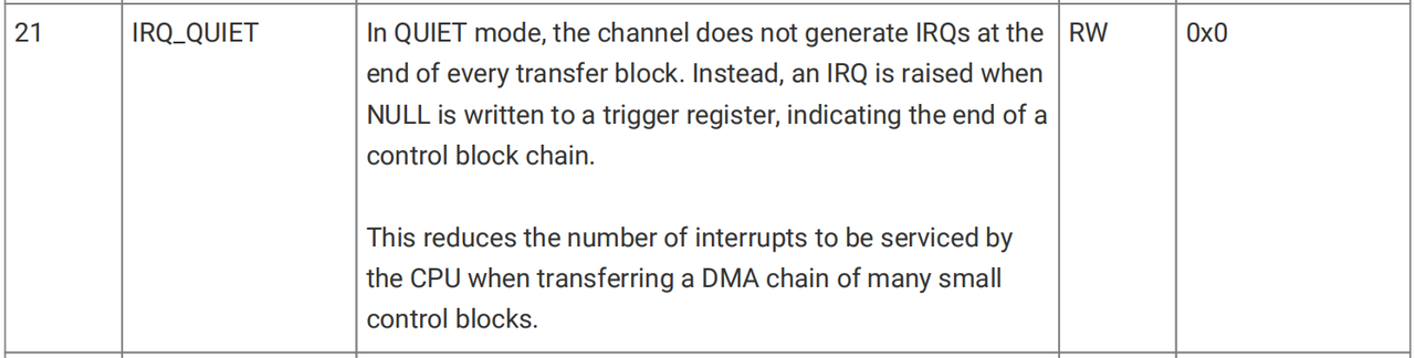
IRQ_QUIET bit‑field inside CTRL register.
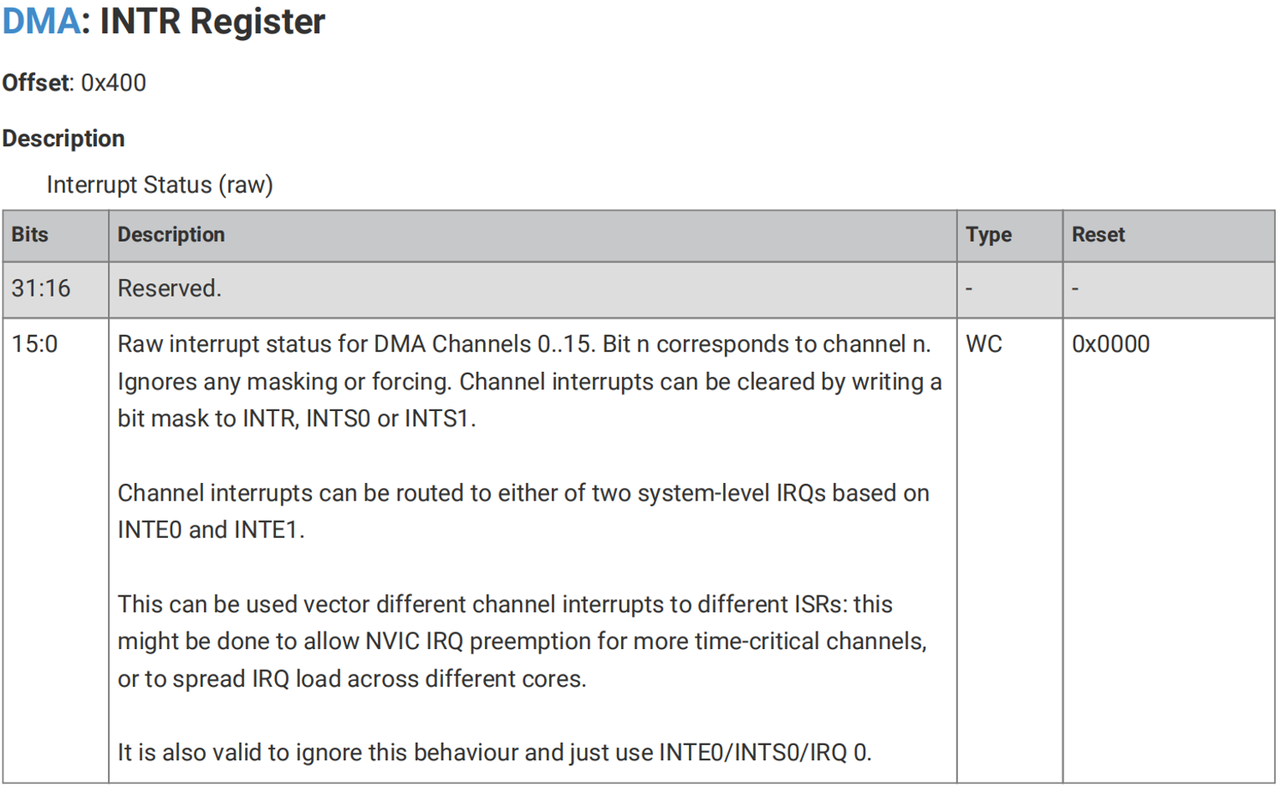
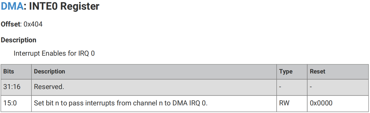
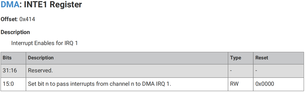
RP2040 DMA exposes two independent system‑IRQ paths with separate mask and status registers (INTE0, INTE1). DMA‑channel interrupt sources can be routed to either IRQ for priority tuning or multi‑core workload partitioning.
INTR register holds raw interrupt status bits for channels 0‑15.
INTS register shows masked interrupt status. Write bit‑mask value to INTS register to clear pending interrupts.
INTE registers implement per‑channel interrupt masking; software enables or disables interrupt‑sources by setting / clearing bits.
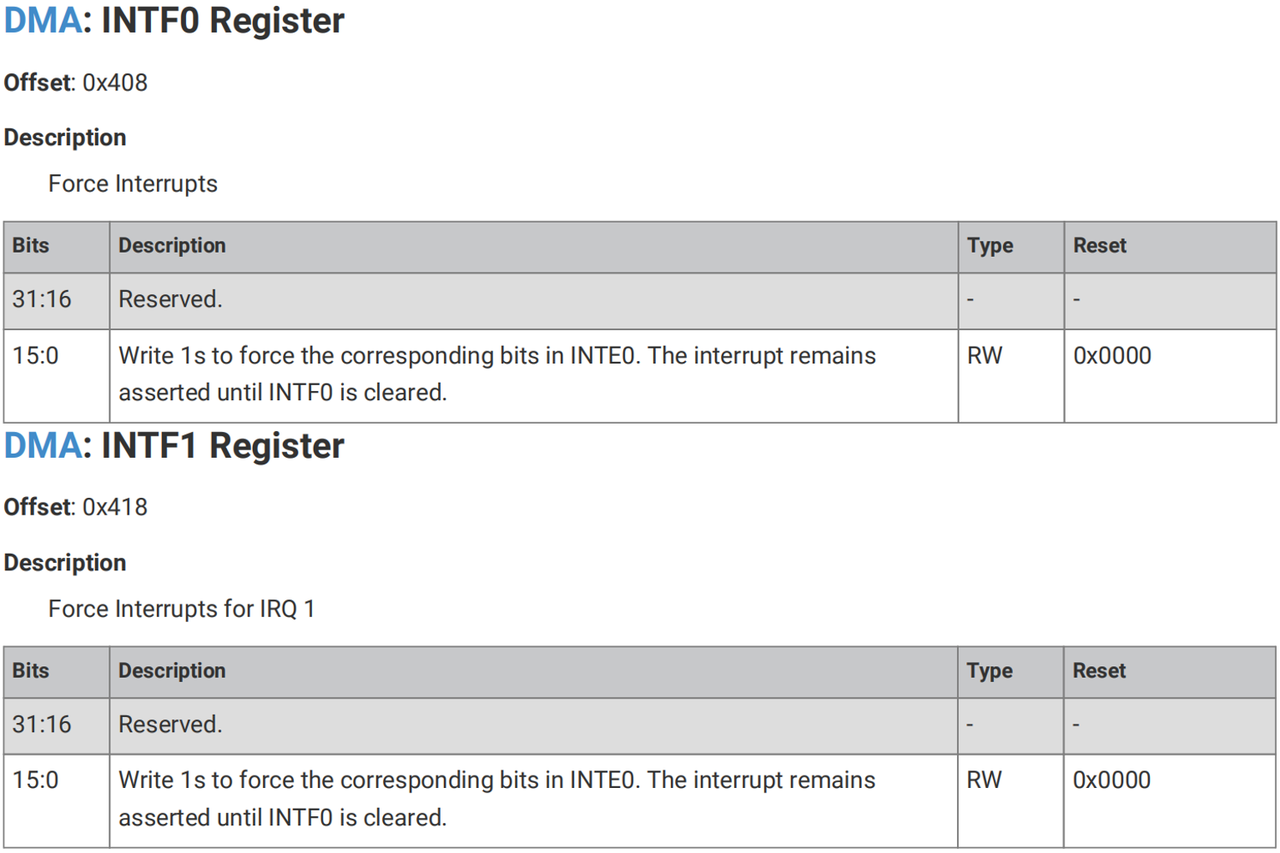
INTF register forces DMA interrupt assertion for debug purposes.
- Additional DMA Features
6.1 Pacing Timer
RP2040 DMA pacing‑timer generates periodic TREQ data‑request pulses on each sys_clk cycle without peripheral DREQ. Fractional X/Y divider sets request generation frequency.
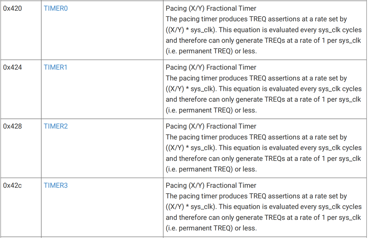
Maximum request rate equals sys‑clock frequency. Effective TREQ rate = ((X / Y) * sys_clk).
6.2 CRC Calculation
DMA integrates CRC calculator operating pass‑through: it observes data flowing through DMA FIFO and computes checksum without modifying payload data. Configure calculation parameters via SNIFF_CTRL register and data handling settings via SNIFF_DATA register.
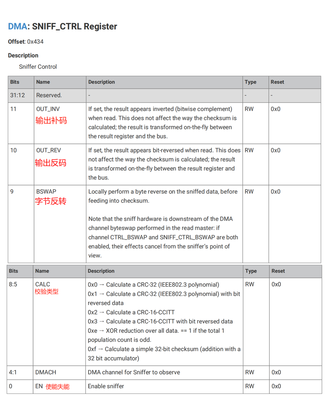
Supported checksum algorithms: CRC‑32, CRC‑16‑CCITT, simple sum, even parity.
6.3 Channel Abort
DMA channels can get stuck under fault conditions e.g. transfer count exceeding peripheral‑buffer capacity. Simply clearing CTRL.EN only pauses operation and cannot fully recover state. Use CHAN_ABORT register for forced recovery without full DMA‑block reset.
Writing bit‑mask to CHAN_ABORT forces selected channels to terminate: transfer‑counter cleared, channel enters idle safe state.
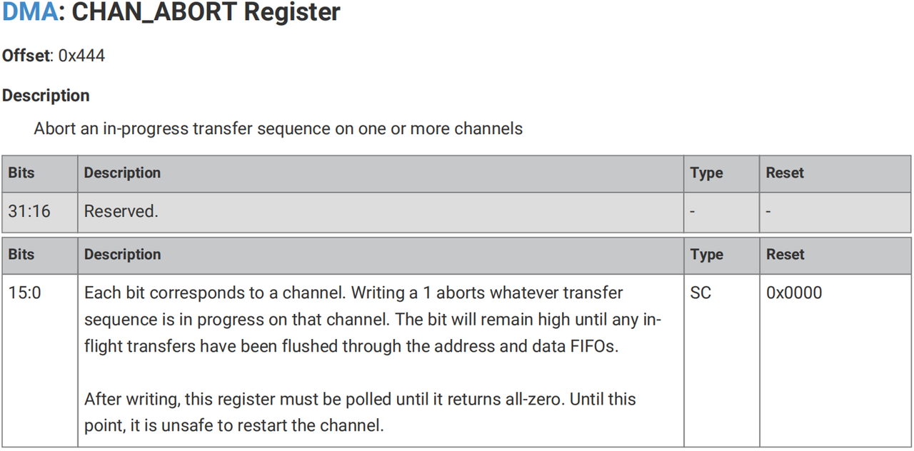
Important hardware note for RP2040: aborting an actively‑running channel may generate completion‑interrupt. Best practice: mask channel‑interrupt before abort; afterwards read and clear interrupt status.
In‑flight bus transactions cannot be cancelled. CTRL.BUSY stays asserted until outstanding bus cycles complete (typically few clock cycles). Do not re‑start channel while BUSY flag remains high; otherwise undefined behaviour occurs.
6.4 Debug Support
Each DMA channel provides debug registers exposing runtime state for diagnostics: DBG_CTDREQ and DBG_TCR. These can also be used for controlled channel reset.
DBG_CTDREQ shows current DREQ counter status.
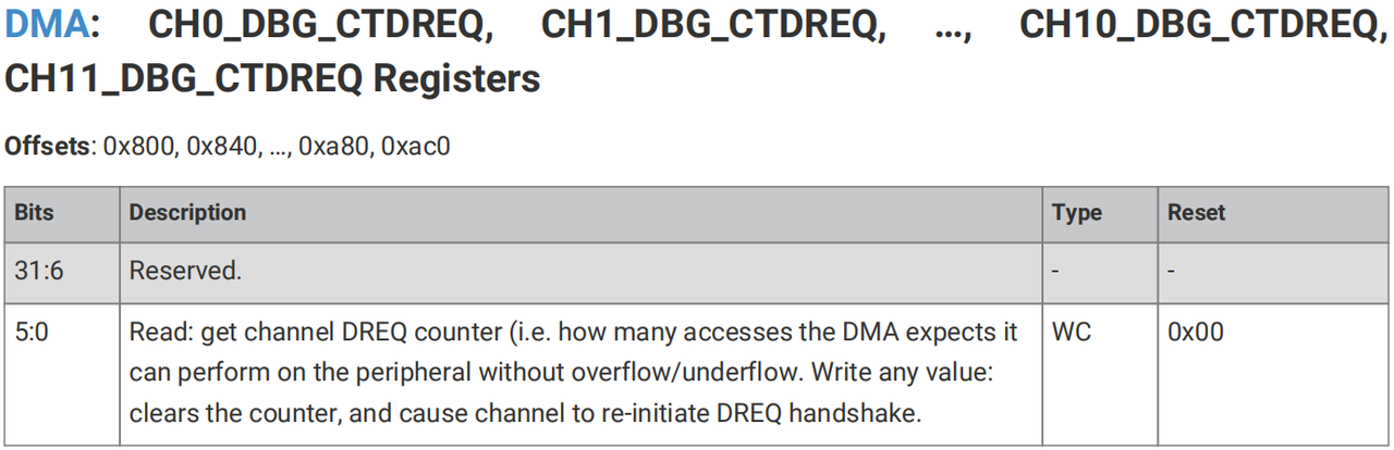
DBG_TCR shows live transfer‑counter value.