Collaborative Architecture of 13 Dual-Core MCUs: A Full Analysis of RP2040's SIO, Interrupts and Eve
This article introduces RP2040's dual-core processor subsystem, covering SIO, interrupts, event signals and SWD debug architecture.
COMPONENTS
PROJECT DESCRIPTION
Processor Subsystem
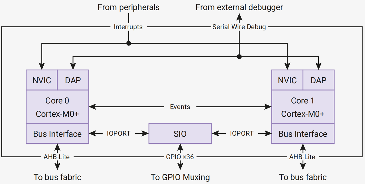
The RP2040 processor subsystem consists of two Arm Cortex-M0+ processors, each equipped with standard internal Arm CPU peripherals as well as external peripherals for GPIO access and inter-core communication.
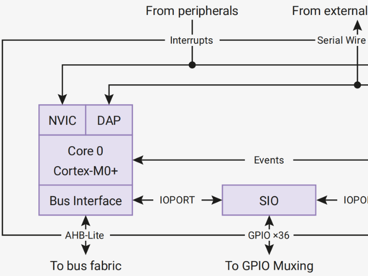
Figure 2.11 Architecture Block Diagram of RP2040 Processor Subsystem
The figure above illustrates the "operating connection framework" of the RP2040 dual-core processor — it defines the communication modes between the two Cortex-M0+ cores (Core0, Core1), other on-chip modules and external devices, serving as the fundamental supporting structure for the dual-core cooperative operation. The functions of the core communication interfaces are as follows:
Independent AHB-Lite Bus Interface: Each core is equipped with a dedicated 32-bit AHB-Lite bus, which serves as its "exclusive main artery" for accessing memory and peripherals — for instance, when Core0 reads SRAM programs or Core1 configures UART peripherals, both operations are routed through their respective buses to the Bus Fabric. This independent bus design eliminates "traffic congestion" caused by dual-core resource contention, ensuring efficient read and write operations for both code and data.
SIO Block and IOPORT: High-Speed GPIO Access + Dual-Core Collaboration SIO is a "high-speed interface block" dedicated to dual-core systems, with each core connected to the SIO via an IOPORT:
On the one hand, it provides "high-speed, zero-latency access" to GPIO — this method delivers faster response and more stable timing compared to accessing GPIO via a bus (for example, it can ensure precise rhythm when rapidly controlling LED blinking);
On the other hand, SIO is also responsible for the "Events communication" between the two cores, enabling Core0 and Core1 to send signals to each other (for example, after Core0 completes Data Acquisition, it sends an event notification to Core1 for processing), so as to realize dual-core collaboration.
Interrupt System: Division-based Response to Spontaneous Tasks Peripherals (such as sensor triggers, serial port data reception) generate interrupt signals, which are routed to the NVIC (Nested Vectored Interrupt Controller) of the two cores. The 26 system-level interrupts of the RP2040 can be assigned to either core for processing; for example, the interrupt for "serial port data reception" can be allocated to Core0, and the interrupt for "sensor trigger" to Core1, enabling the dual cores to respond to sudden tasks in a divided manner and improving the real-time performance of the system.
SWD Debug Bus: A Unified Entry Point for External Debugging An external debugger connects to the DAP modules of both cores simultaneously via a multi-drop Serial Wire Debug bus — this means the external debug host can access and debug Core0 and Core1 at the same time. For example, when a program malfunctions, the operating status of both cores can be viewed concurrently, enabling precise localization of issues arising in dual-core collaboration.
Next, we will introduce these key parts one by one.
1.Single-cycle IO block (SIO)
SIO is the "high-speed collaboration toolbox" for the dual-core RP2040 processor — it leverages the Cortex-M0+ IOPORT auxiliary bus to deliver "single-cycle (ultra-fast)" operations, and is purpose-built to handle time-critical and speed-sensitive tasks such as high-speed inter-core data transfer, shared resource contention management, and high-speed GPIO control, serving as the core supporting module for efficient dual-core collaboration.
The essence of SIO is a "fast lane module" based on the IOPORT auxiliary bus: IOPORT is a dedicated fast bus port of Cortex-M0+, corresponding to the address range starting from 0xd0000000, which can be accessed with common read and write instructions. Moreover, SIO is not connected to the main system bus and only runs through this fast lane — this ensures that all read and write operations of SIO can be completed within 1 cycle, featuring high speed and precise timing.
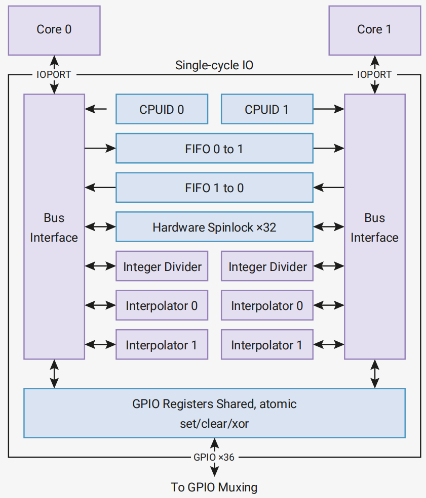
The specific structure of SIO is shown as follows:
The specific structure of SIO is shown as follows:
SIO uses the auxiliary bus IOPORT of Cortex-M0 for 32-bit access, which is designed to save access time, execute high-speed computing tasks, and can also be used for inter-core communication between two cores.
IOPORT is an auxiliary bus port on the Cortex-M0+ that can perform fast 32-bit read and write operations.
Processors access their IOPORTs using normal load and store instructions, pointing to the special IOPORT address range 0xd0000000.. .0xdfffffff. The SIO appears as memory-mapped hardware in the IOPORT space.
SIO has a dedicated bus interface for the IOPORT of each processor. Due to its strict timing requirements, SIO is not connected to the main system bus, and it can only be accessed by the processor or a debugger via the processor debug port.
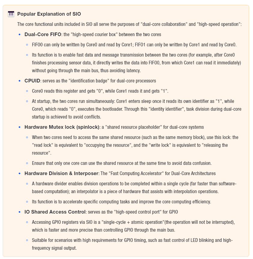
Both read and write operations of SIO are completed in one cycle, consisting of the following units:
Dual-core FIFO: Used to transfer data, messages or ordered events between two cores
One of the FIFOs can only be written by core 0 and read by core 1
The other one can only be written by core 1 and read by core 0
CPUID: Used to identify the currently operating core, the CPUID register is the first register in the IOPORT space. When accessing this address, core 0 reads a value of 0, while core 1 reads a value of 1. The software determines which core it is running on during the initial boot process: both cores start running simultaneously, core 1 enters a deep sleep state, and core 0 continues to execute the main boot sequence.
Hardware Mutex Lock: It can be used to manage mutually exclusive access to shared software resources, and software interacts with each spin lock through one of the following operations
Read: i. e., acquire the lock
Write: Release the lock
Hardware division and interpolator
IO Shared Access Control
2. Interrupt
Interrupts are the core mechanism for the RP2040 to handle "burst tasks" — for instance, when a timer expires, data is received via a serial port, or a sensor triggers a signal, the core cannot wait to "finish its current work" before processing these events; at such times, an interrupt will "interrupt" the core's ongoing operation to prioritize the urgent task. The NVIC (Nested Vectored Interrupt Controller) acts as the "interrupt scheduler" for each core, responsible for managing interrupt priorities and execution sequences. The following will explain its logic clearly with reference to the table and relevant rules:
Each core (Core0 and Core1) has an independent NVIC, which acts as a dedicated "interrupt dispatcher". It can receive 32 interrupt signals, but the RP2040 only uses the first 26 of them (IRQ0 to IRQ25), while the remaining IRQ26 to IRQ31 are reserved (and can also be forcibly triggered). When a peripheral (such as a timer or UART) triggers an urgent task, it sends a signal to the corresponding IRQ, and the NVIC then schedules the core to process it.
On the RP2040, only the lower 26 IRQ signals are connected to the NVIC, while IRQs 26 to 31 are not wired. By writing bits 26 to 31 in the NVIC ISPR register, the core can still be forced to enter the corresponding interrupt handler.
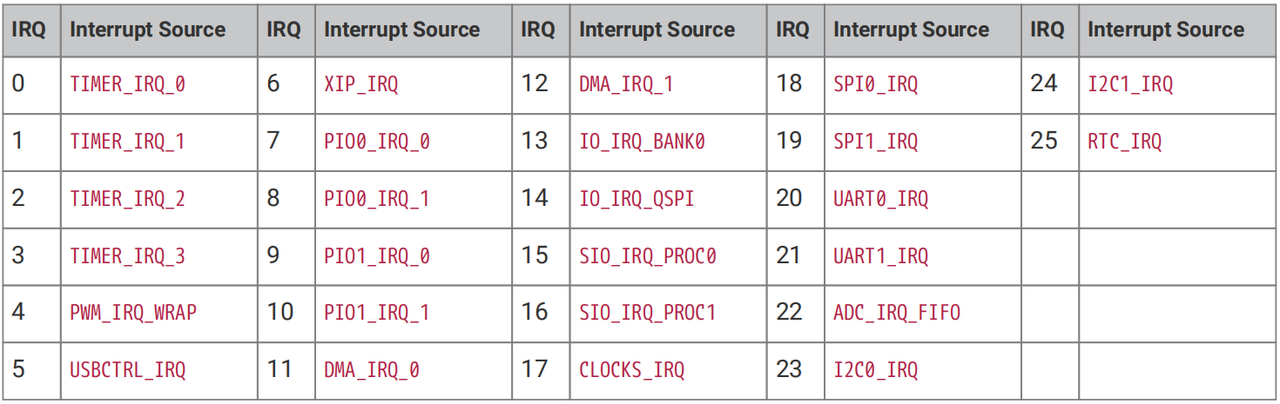
The interrupt vector table of RP2040 is as follows. This table acts as the "task list for IRQs", where each IRQ number corresponds to a specific "source of urgent tasks":
Figure 2.13 RP2040 Interrupt Source to IRQ Mapping Table
For example, IRQ0 corresponds to "IRQ of Timer 0"(meaning Timer 0 has timed out), and IRQ20 corresponds to "IRQ of UART0"(meaning UART0 has received data). Once the core sees the IRQ number, it can immediately identify which peripheral has sent the "urgent call" and then invoke the corresponding handler.
When multiple IRQs are triggered simultaneously, the core processes them in sequence according to their "urgency level", with priority determined in two layers:
NVIC dynamic priority: Each IRQ can be assigned 4 priority levels (0 to 3) via registers, with a smaller number indicating a higher urgency level (for example, level 0 is the highest priority and will be processed before level 1);
IRQ Number Priority: If two IRQs have the same NVIC priority, the IRQ number will be the deciding factor — the smaller the number, the higher the urgency (for example, IRQ0 has a higher priority than IRQ1).
Hardware supports nested interrupts: a low-priority interrupt can be preempted by a high-priority interrupt (or another exception such as a hard fault), and the low-priority interrupt will resume once the high-priority exception is completed. This "cutting in line" mechanism ensures that the most urgent tasks are always responded to first.
3. Event Signals
First, clarify the core concepts:
Event signal: It is a lightweight "wakeup/notification signal. The difference between it and an interrupt is that an interrupt " interrupts the core's current work" to handle urgent tasks, whereas an event mainly " wakes up a core in sleep state" or " sends a notification to another core", and will not actively interrupt the core's operation.
WFE instruction: Short for Wait For Event, this instruction will put the core into a sleep state and suspend its operation once executed, and the core will not be woken up until an event or interrupt arrives.
SEV instruction: Short for Send Event, when executed by the core, this instruction can actively generate an event signal to notify or wake up other cores.
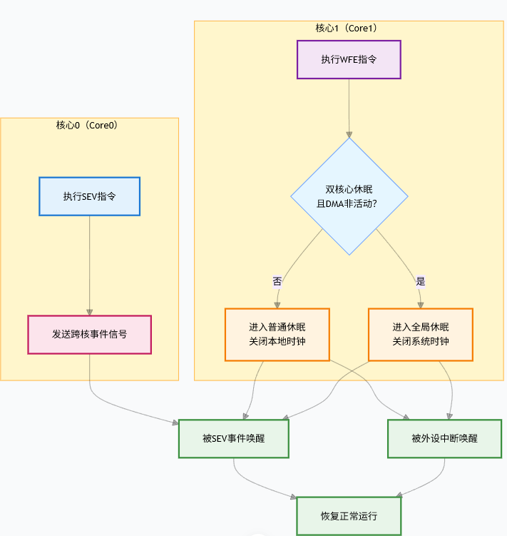
In the RP2040, the event signal serves as a core mechanism for dual-core coordination and low-power sleep, with its logic outlined as follows:
Event intercommunication between dual cores:
The event signals between the two cores (Core0 and Core1) of the RP2040 are "cross-connected" — for example, when Core0 executes the SEV instruction to send an event, this event will be received by Core1; conversely, events sent by Core1 can also be received by Core0.
The purpose of this design is to implement "lightweight notification between dual cores": for example, after Core0 completes Data Acquisition, it sends an event to wake Core1 which is in sleep state to let it continue processing data, which not only avoids the waste of computing power caused by core idling, but also is more lightweight than using interrupt for notification.
Implementation of low-power sleep mode:
When the core enters sleep mode by executing the WFE (or WFI, wait for interrupt) instruction, its internal clock gate is turned off, so no additional power is consumed; if both cores enter sleep state and the DMA is also inactive, the entire RP2040 will enter "global sleep", which simultaneously shuts down the clocks of unused modules to further reduce power consumption.
The trigger conditions for wake-up are highly flexible: whether it is an event sent by another core or an interrupt triggered by a peripheral, it can wake the core (or the entire chip) from sleep and resume operation — this is extremely practical in scenarios requiring low power consumption, such as battery-powered devices.
4. Debugging
Before understanding the debugging structure, let's first clarify several core concepts:
SWD (Serial Wire Debug): a debug interface that requires only two wires (the SWCLK clock line and the SWDIO data line), serving as the "channel" for communication between an external debugger (such as a debugging tool on a computer) and the internal modules of a chip, and is used to implement operations including program downloading and debugging.
DAP (Debug Access Port): it serves as the "debugging entry point" inside the chip, and each core (Core0, Core1) corresponds to one DAP (DAP_0, DAP_1); an external debugger can access the operating status of the cores and control their execution via the DAP.
SWD Multi-node Arbiter: It acts as the "traffic controller" for debug communication — the external debugger only has one SWD interface, yet it needs to connect to the DAPs of two cores and the backup rescue port. The arbiter is responsible for allocating communication resources to prevent signal conflicts caused by multiple debug access points competing for the same line.
Rescue DP (Rescue Debug Port): serves as the "safe exit" for debugging — when normal DAP debugging fails (e. g., the core is stuck), this backup port can be used to restore debugging functionality.
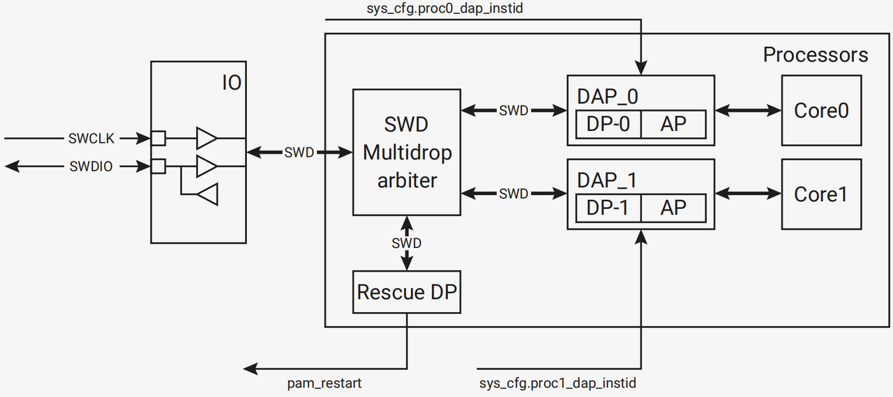
Figure 2.15 Block Diagram of RP2040 SWD Serial Wire Debug Architecture
This diagram illustrates the debug communication architecture of the RP2040, which implements the unified control of dual-core by an external debugger plus debug reliability guarantee, with the core logic as follows:
Basic Communication of the SWD Interface: An external debugger connects to the chip's IO module via the two lines SWCLK and SWDIO, then accesses the SWD multi-node arbiter — this is the only communication channel between the debugger and the chip's interior. It is recommended to use a maximum frequency of 24MHz to ensure stable communication.
Debug Resource Scheduling (Role of the Arbiter): Since there are 2 core DAPs inside the chip (DAP_0 corresponds to Core0, DAP_1 corresponds to Core1) and 1 Rescue DP, while the debugger only has 1 SWD interface, the arbiter will allocate communication to the corresponding port based on debugging requirements:
To debug Core0, assign it to DAP_0;
To debug Core1, assign it to DAP_1;
When normal debugging fails, the relevant resources will be allocated to Rescue DP. This can prevent multiple debugging entry points from competing for signals and ensure orderly communication.
Core Functions of SWD Debugging Through this architecture, an external debugger can perform the following operations:
Load programs (firmware) to the SRAM of the chip or external flash memory;
View / modify the core operating status (e. g., register values);
Core Execution Control: It enables running and stopping the core, executing code step by step, and setting breakpoints (to pause the core when it reaches the specified code).
The "rescue" guarantee of Rescue DP When normal DAP debugging becomes unavailable due to core lockup, configuration errors or other issues, Rescue DP serves as a backup entry to restore debugging functionality via the pam_restart signal — this is a security mechanism that prevents the chip from being "bricked" due to debugging failures.