ADS1115 Explained: Registers, Modes & I2C Timing
ADS1115 peripheral deep analysis
- ADS1115 Chip Introduction
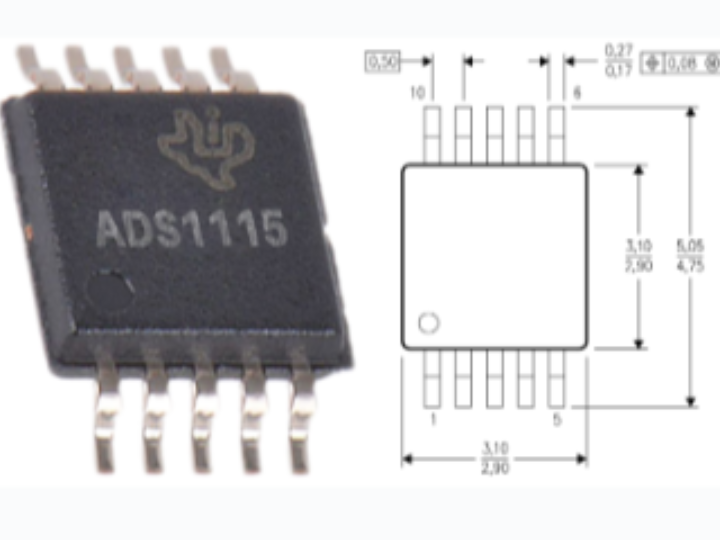
ADS1115 is a high‑precision, low‑power 16‑bit Analog‑to‑Digital Converter (ADC) produced by Texas Instruments (TI). It integrates multiple functions and is suitable for various analog‑signal acquisition and processing applications such as sensor interfaces, voltage monitoring and portable devices. The ADS1115 communicates with microcontrollers via the I²C interface. Its pins include power supply pins (VDD, GND), SCL and SDA for I²C communication, the ADDR pin for device address configuration, and A0~A3 as analog‑input pins.
Key specifications:
Resolution 16‑bit for high‑precision data conversion.
Programmable sampling rate Up to 860 samples per second (SPS), adjustable according to application requirements.
Input configuration Integrated input multiplexer (MUX) supporting four single‑ended inputs or two differential inputs.
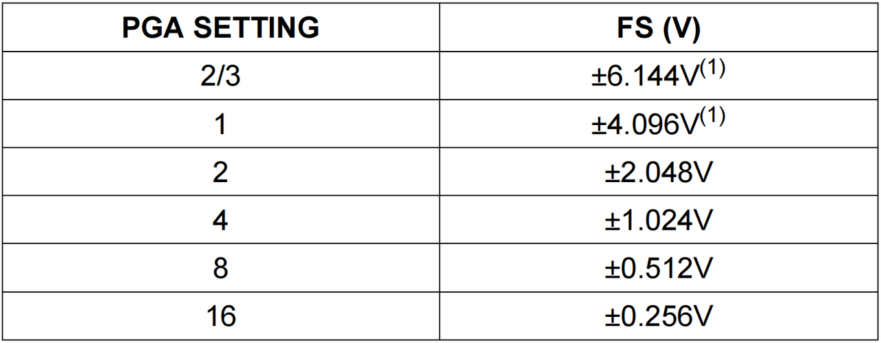
Programmable Gain Amplifier (PGA) On‑chip PGA with adjustable gain range (±6.144 V to ±0.256 V) to extend measurable signal range.
Interface Standard I²C interface. Multiple‑device connection is supported via address selection using the ADDR pin.
Low power consumption Approximately 150 μA supply current under continuous‑conversion mode; standby current is further reduced in single‑shot mode.
Wide power‑supply range Operates from 2.0 V to 5.5 V.
Internal low‑drift reference voltage Provides stable reference voltage to guarantee high‑accuracy analog‑to‑digital conversion.
Internal oscillator On‑chip oscillator removes dependency on external clock sources.
- ADS1115 Internal Block Diagram and Pin Description
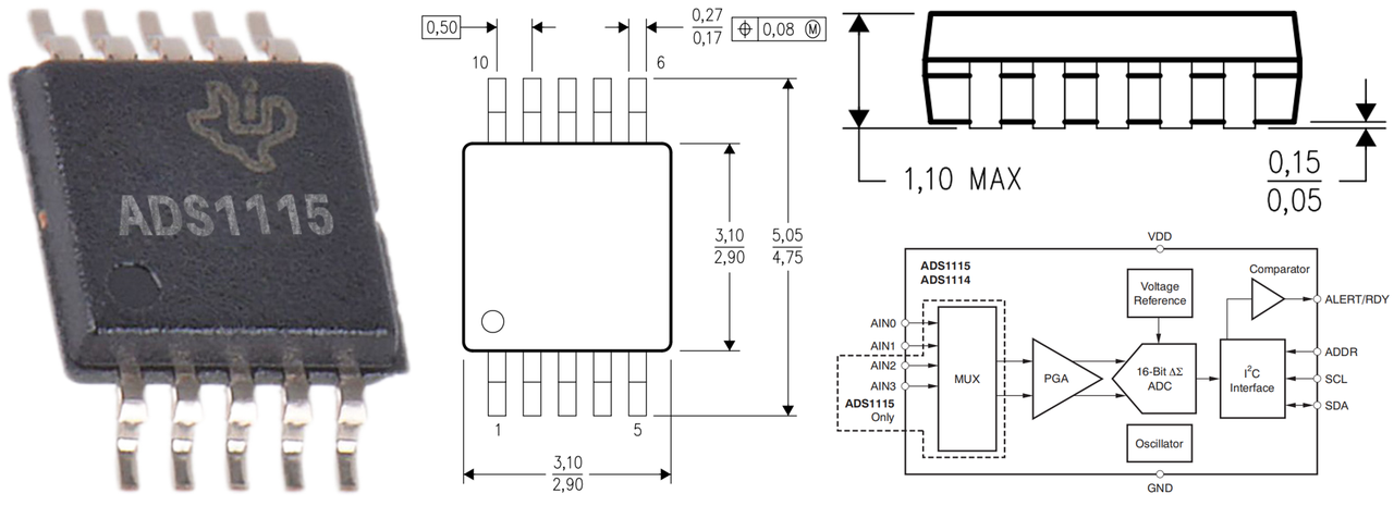
ADS1115 pinout:
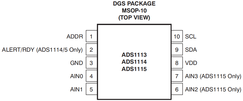
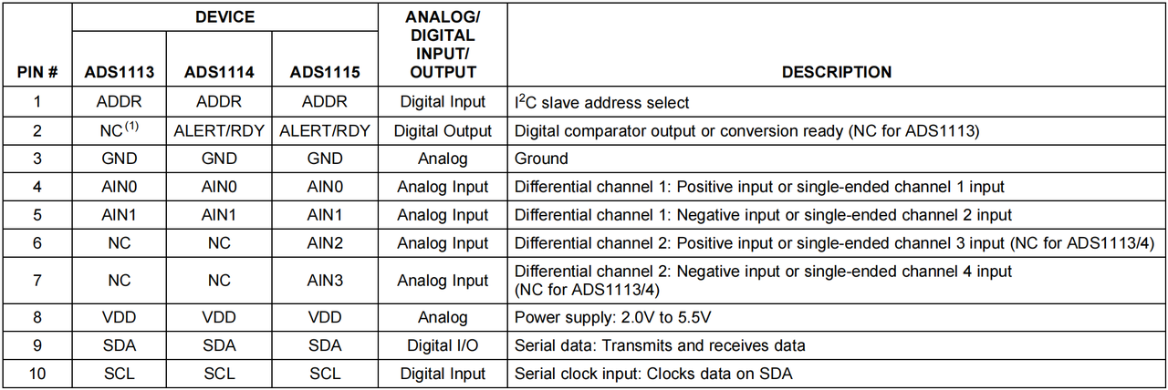
Pin‑by‑pin functions:
VDD (Power‑supply pin) Supply voltage ranges from 2.0 V to 5.5 V, maximum operating current 150 µA.
GND (Ground pin) Ground reference potential.
SCL (Serial clock pin) I²C clock line. Input high‑level: 0.7 × VDD ~ VDD+0.3 V; input low‑level: 0 V ~ 0.3 × VDD. Supports communication speed up to 400 kHz. Requires external pull‑up resistor (typical value 4.7 kΩ).
SDA (Serial data pin) I²C data line. Electrical specifications are identical to SCL; external pull‑up resistor is required.
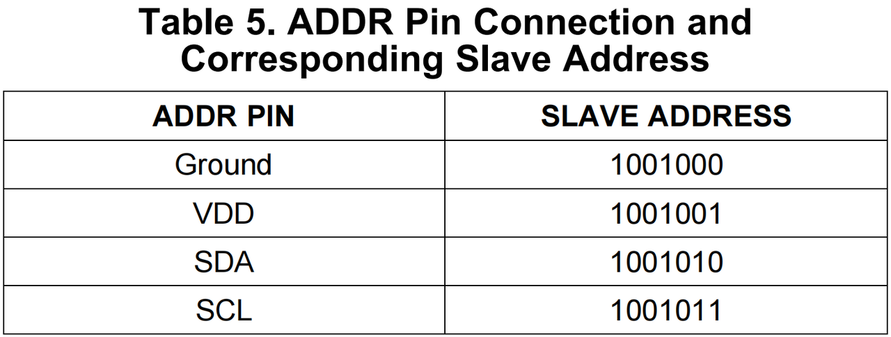
ADDR (Address‑selection pin) Sets the I²C slave address of ADS1115. Four distinct I²C addresses can be selected through different wiring configurations.
ALERT/RDY (Interrupt / Ready pin) Configurable as comparator‑interrupt output or data‑conversion‑complete indicator. Open‑drain output; external pull‑up resistor is mandatory.
AIN0, AIN1, AIN2, AIN3 (Analog‑input channels) Four analog‑input channels for single‑ended or differential measurements. Input voltage must not exceed VDD+0.3 V nor drop below GND‑0.3 V. Valid input range is also affected by PGA configuration.
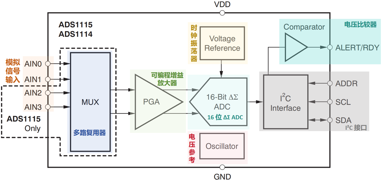
ADS1115 internal block diagram:
Internal functional units:
MUX (Multiplexer) Configurable multiplexer for selecting differential or single‑ended measurements among AIN0‑AIN3 input channels.
PGA (Programmable Gain Amplifier) Amplifies input signals and feeds them to the 16‑bit ΔΣ ADC. Gain is configurable to adapt to different input‑signal amplitudes.
I²C interface Communicates with external MCU via standard SCL / SDA signals. The ADDR pin sets device address, allowing multiple ADS1115 chips on one I²C bus.
Comparator Optional comparator function working together with the ALERT/RDY pin to assert interrupts upon data readiness or threshold crossing events.
16‑bit ΔΣ ADC Converts analog‑input signals into 16‑bit digital values and transmits results over the I²C interface.
Internal voltage reference and clock oscillator Provides stable on‑chip clock and voltage reference for precise analog‑to‑digital conversion.
2.1 Multiplexer
The built‑in multiplexer (MUX) selects which input channel is measured. Two primary signal‑connection modes are supported: differential input and single‑ended input.
Differential input Measures voltage difference between two pins (positive input and negative input). For ADS1115, it measures the voltage between AINP (positive input) and AINN (negative input). Differential mode accepts both positive and negative voltages within ±Vref full‑scale bipolar range and makes full use of all 16 ADC bits. Full‑scale range is divided into 2^16 = 65536 discrete levels. Resolution equals 2*Vref / 65536.
Single‑ended input Signal is applied to one channel while the other channel is tied to GND. The ADC measures input voltage relative to ground. Single‑ended mode only accepts positive voltages from 0 to Vref (unipolar range). Only 15 bits are effectively used, resulting in one‑bit resolution loss. Full‑scale range yields 2^15 = 32768 discrete levels. Resolution equals Vref / 32768.
A multiplexer acts as an electronic switch that selects one signal source for output among multiple inputs.
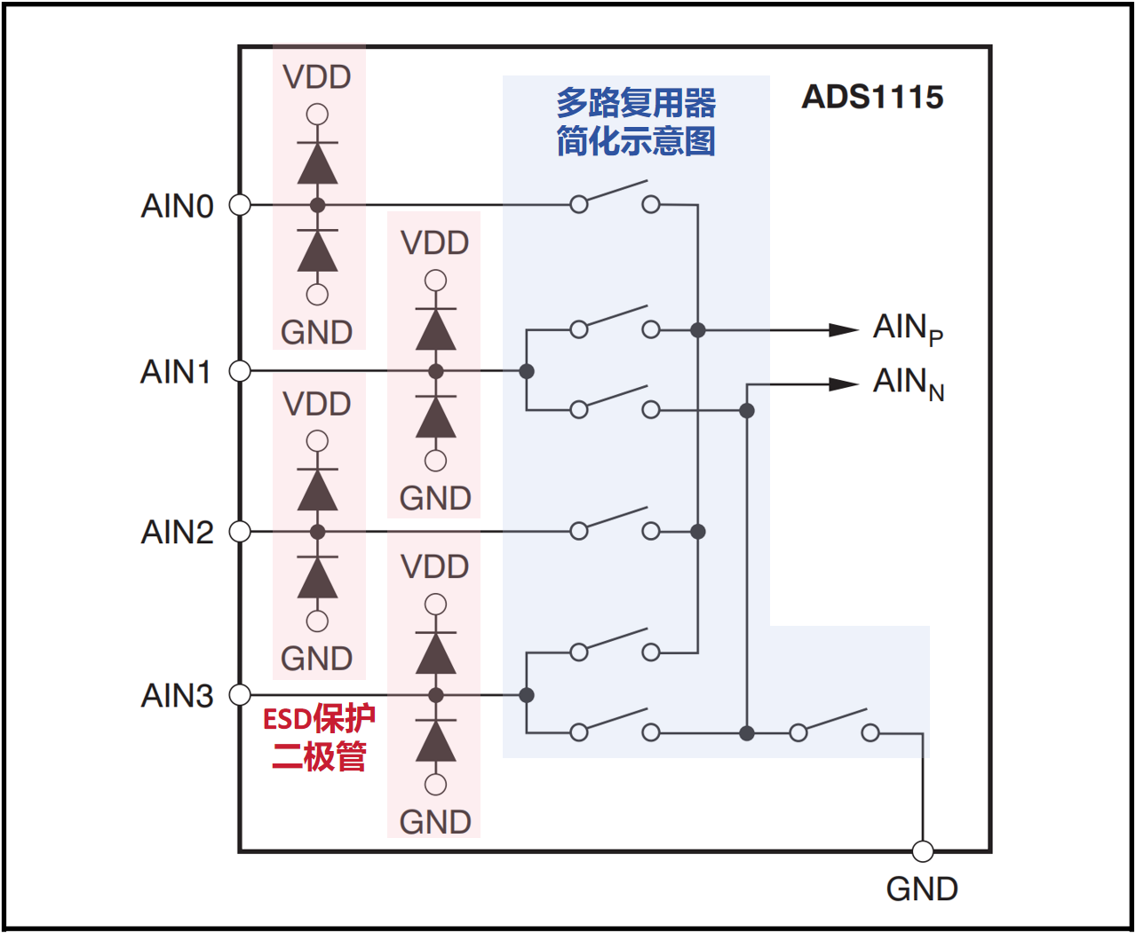
By configuring MUX bits in registers, ADS1115 selects input mode. For single‑ended measurements, MUX internally connects the ADC negative‑input terminal (AINN) to GND.
ADS1115 analog‑input pins include ESD protection diodes safeguarding inputs against over‑voltage and negative‑voltage stress. To prevent these diodes from conducting, input voltages must satisfy: GND - 0.3V < AINx < VDD + 0.3V
If input signals may exceed these limits, external Schottky diodes or series resistors are recommended to limit input current and protect the ADC. When unused input channels could be over‑driven (voltage outside valid range), they may corrupt conversion results of other channels. Voltage clamping (e.g. Schottky diodes) for unused channels is advised.
2.2 Analog‑signal input
ADS1115 uses a switched‑capacitor architecture for differential‑voltage measurement. Sampling relies on timing‑controlled closing and opening of switches S1 and S2 to charge and discharge sampling capacitors.
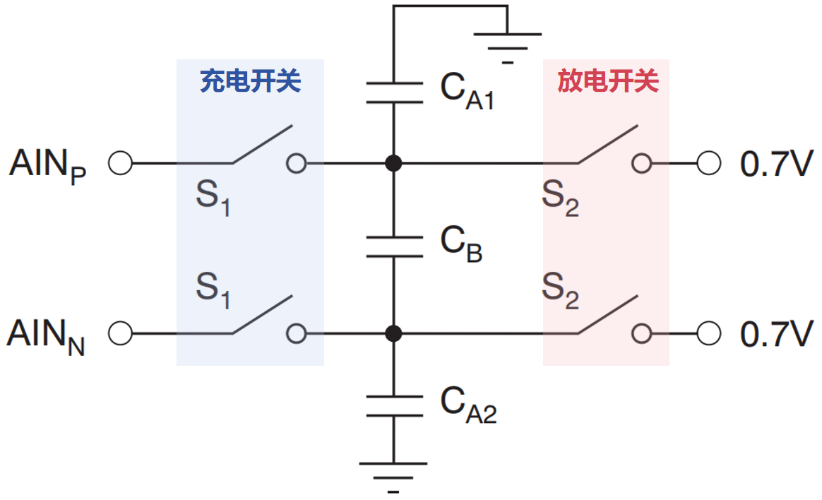
S1 is the charge switch; S2 is the discharge switch.
S1 charge switch Controls capacitor sampling from AINp / AINn inputs. When S1 closes, the capacitor charges to the instantaneous voltage at AINp / AINn. When S1 opens, the capacitor holds the sampled voltage and prepares for the discharge phase.
S2 discharge switch Closes after S1 opens to start discharge. Capacitor charge is dumped toward reference potential (typically 0.7 V or 0 V), preparing hardware for the next sampling cycle.
Capacitor charge‑discharge cycles generate small transient currents. Average current can be used to calculate effective ADC input impedance:
$$ \text{Effective Input Impedance (}Z_{\text{in}}\text{)} = \frac{V_{\text{IN}}}{I_{\text{AVERAGE}}} $$
Where $V_{\text{IN}}$ is input voltage and $I_{\text{AVERAGE}}$ is average input current. Different PGA gain settings change full‑scale ADC range and also alter effective input impedance.
2.3 PGA Programmable Gain Amplifier
A Programmable Gain Amplifier dynamically adjusts amplification factor under external control to fit input‑signal amplitude into the ADC measurable range.
Major internal PGA building blocks:
Gain‑control circuit Usually implemented with resistor networks and switch matrices. Different resistor combinations set amplification factors.
Feedback circuit Negative‑feedback loops guarantee amplifier stability. Feedback‑resistor values control output gain magnitude.
Differential input and output Differential topology suppresses noise and common‑mode interference.
Amplifier core Operational amplifier performing actual signal amplification according to configured gain.
Example illustrating PGA function and input‑range impact: Assume a sensor output fluctuates near 0.001 V while the target ADC accepts 0~5 V with 10‑bit resolution. One LSB step equals 5 V / 1024 = 0.00488 V. Raw ADC readings would always return zero; tiny sensor variations cannot be detected.
Adding a PGA amplifying the input signal by 100× expands signal swing to 0.1 V. After amplification, ADC output values range from 0 to 20, making signal fluctuations observable.
However, PGA gain narrows the acceptable input‑voltage range. With 100× gain, original 05 V input range shrinks to 00.05 V. Feeding 0.1 V will exceed input limits and produce saturation or signal distortion.
Proper PGA gain selection is critical. Set gain so that amplified signal falls inside the ADC optimal measurement window (for example 0‑3.3 V). Ensure amplified output never exceeds ADC maximum input rating.
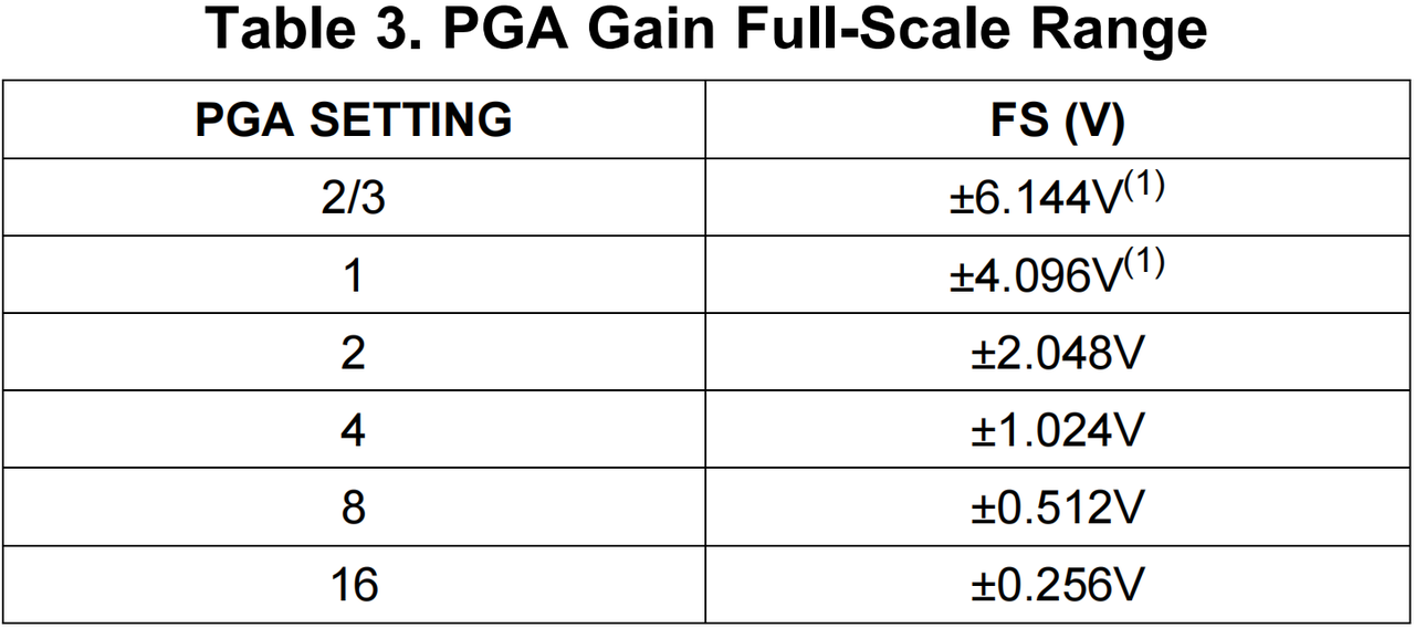
ADS1115 PGA supports multiple gain settings: 2/3, 1, 2, 4, 8, 16. Each gain setting changes full‑scale analog‑input range.
2.4 ADC Conversion Unit
ADS1115 stores conversion results in two‑complement binary format.
When input reaches maximum positive value, result register holds 7FFFh (decimal 32767); values beyond this level will not further change register content.
When input reaches maximum negative value, result register holds 8000h (decimal -32768); more negative inputs leave register unchanged.
Minimum achievable resolution depends on PGA gain because full‑scale range changes with gain selection.
Input‑voltage‑to‑code transfer characteristics:
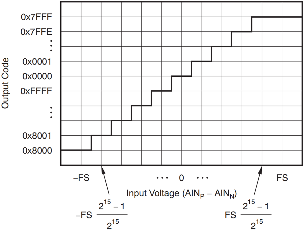
To avoid aliasing, ADC sampling rate must be at least twice the highest input‑signal frequency. The on‑chip digital filter attenuates high‑frequency noise to some degree. External analog filters may still be required for certain applications. Input‑filter network design must consider interaction with ADS1115 input impedance.
ADS1115 ADC supports two operating modes: continuous‑conversion mode and single‑shot conversion mode.
Continuous‑conversion mode The chip repeatedly executes analog‑to‑digital conversions. After finishing one conversion, result is latched into the conversion register and the next conversion immediately starts.
Single‑shot conversion mode Conversion is triggered by setting the OS bit high inside the configuration register. OS bit clears while conversion is in progress. Once conversion completes, OS bit sets again and the device enters low‑power standby state.
2.5 Internal Voltage Comparator
ADS1115 integrates a configurable voltage comparator.
Traditional comparator mode ALERT/RDY pin asserts when conversion result exceeds high‑threshold register value (active‑low by default). De‑assertion occurs when input falls below low‑threshold register value.
Window comparator mode ALERT/RDY pin triggers if conversion result goes above high threshold OR goes below low threshold.
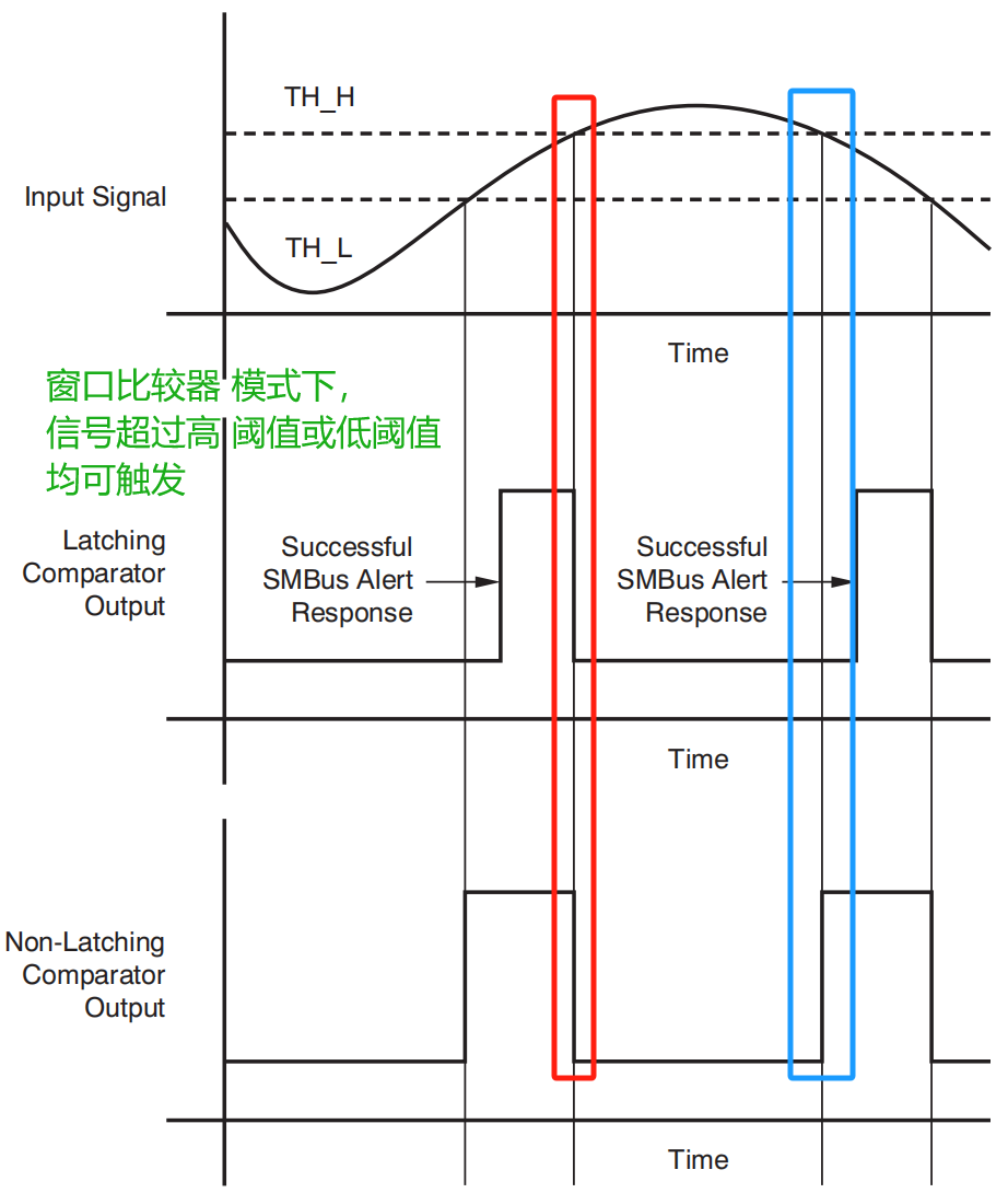
COMP_LAT latch bit configures whether comparator output stays asserted after threshold crossing even if input returns inside normal range. COMP_POL polarity bit selects whether ALERT/RDY is active‑high or active‑low.
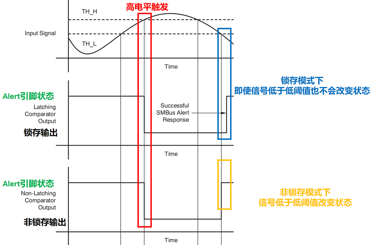
COMP_QUE bits allow triggering after 1 / 2 / 4 successive threshold‑crossing samples. Comparator function can also be fully disabled via COMP_QUE.
Depending on register setup, the ALERT/RDY pin can act as an alarm comparator output or a data‑ready status signal. Refer to comparator threshold‑register section for details.
2.6 ADS1115‑MCU Hardware Connection
Typical application circuit for signal acquisition with ADS1115:
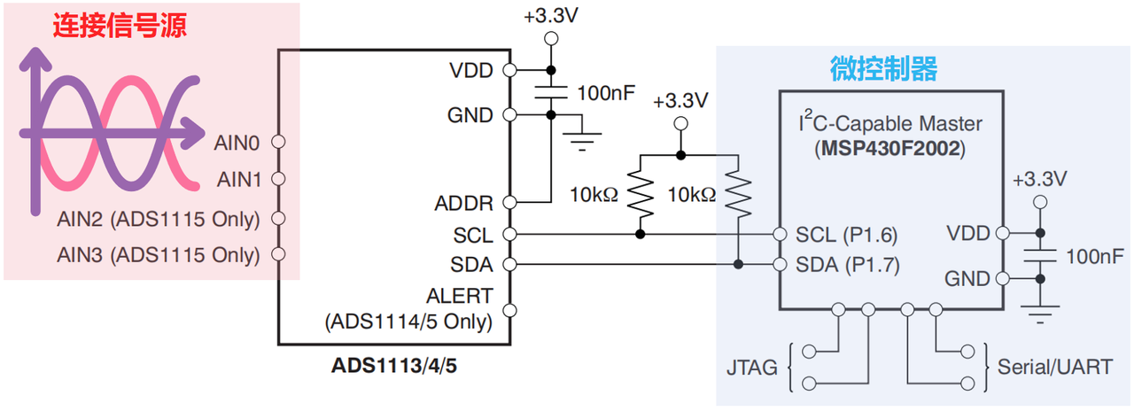
Decoupling capacitor is added on VDD supply pin for stable power. ADS1115 connects to MCU over I2C; ALERT pin also needs external pull‑up resistor.
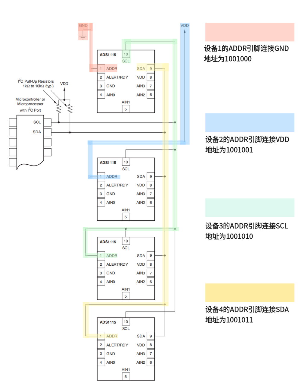
Each ADS1113 / ADS1114 / ADS1115 can be assigned one of four I²C slave addresses using the ADDR pin. Up to four devices may share a single I²C bus.
- ADS1115 Register Overview
ADS1115 register set:
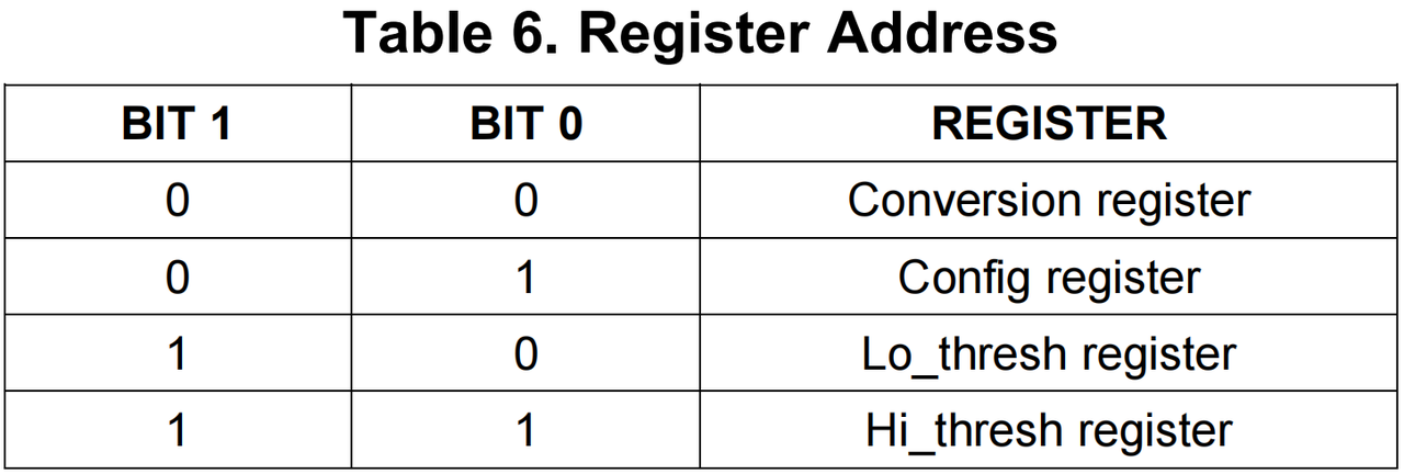
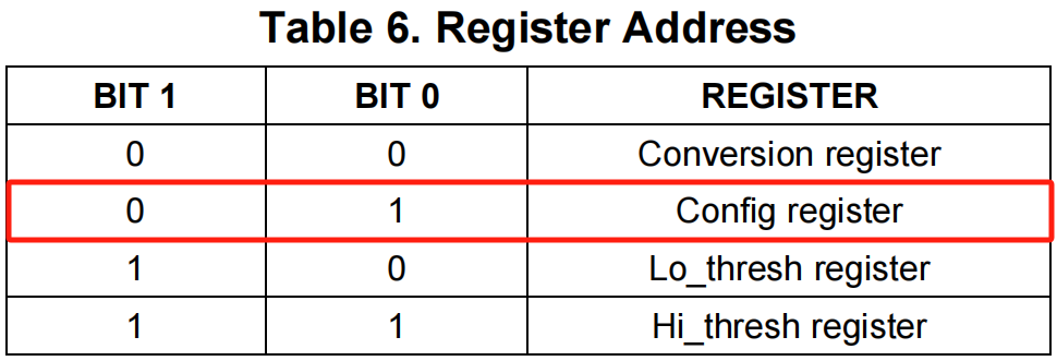
Pointer Register Selects target register for subsequent read or write operations by writing different pointer values.
Config Register Configures chip operating parameters: input‑channel selection, PGA gain, data rate and operating modes.
Conversion Register Holds analog‑to‑digital conversion result.
Lo_thresh and Hi_thresh Registers Set upper and lower threshold levels for the on‑chip voltage comparator.
ADS1115 performs power‑on reset. All configuration‑register bits revert to their default states during reset.
3.1 Pointer Register
Selects target register access; the two least‑significant bits are writable.
Different pointer values select different target registers.
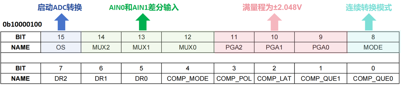
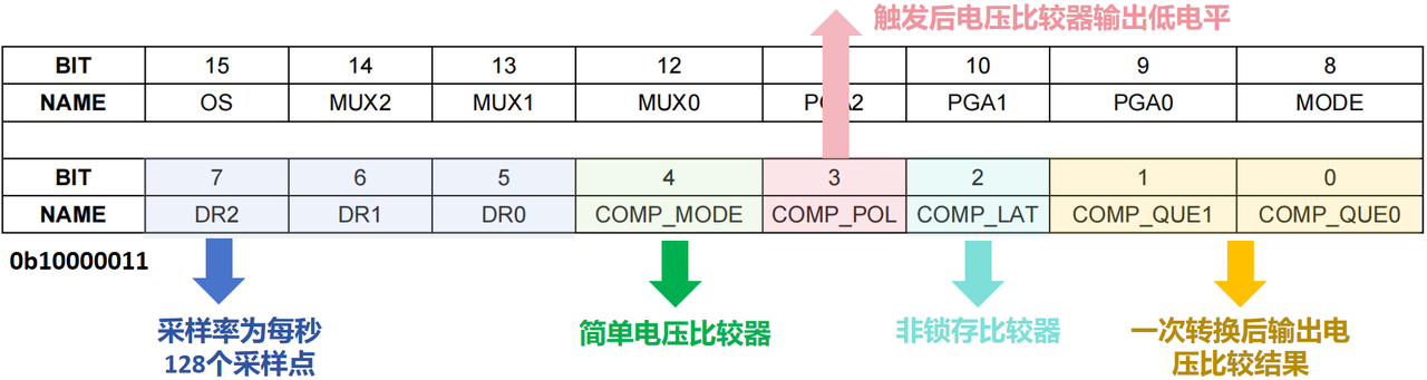
3.2 Config Register
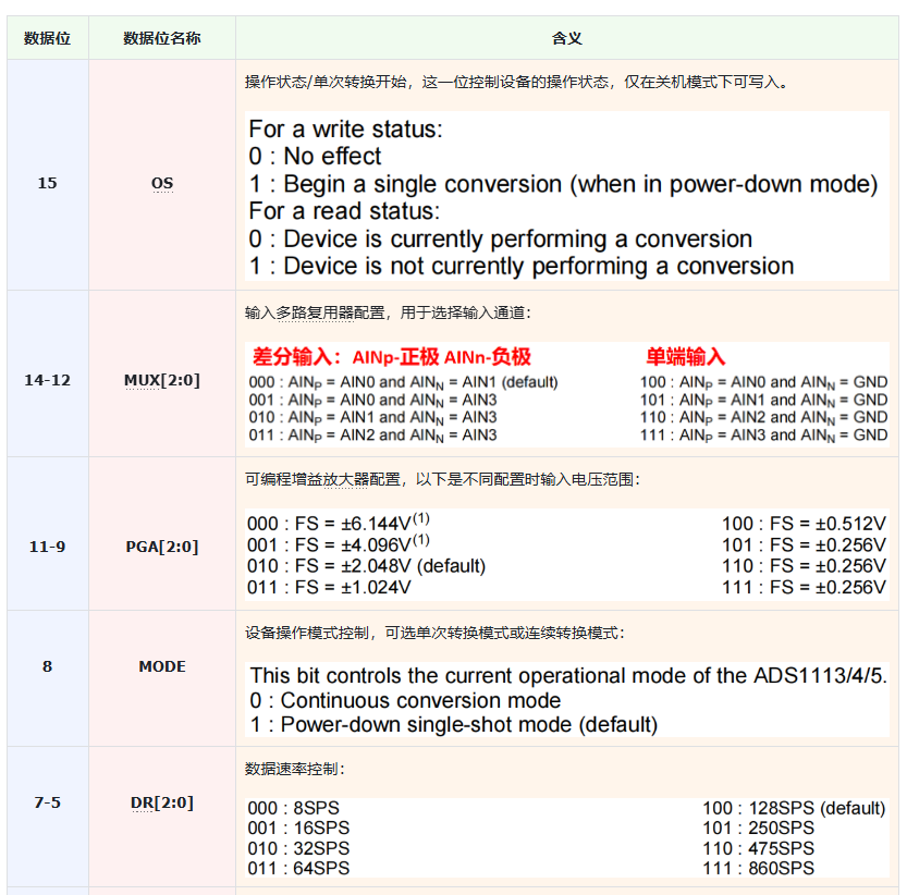
16‑bit read‑write register.

Bit‑field definitions:
3.3 Conversion Register
16‑bit register storing conversion result in two‑complement format. After power‑on, conversion register clears to zero and stays zero until completion of the very first conversion.

3.4 Lo_thresh and Hi_thresh Registers
These two registers store lower and upper threshold values for the internal comparator, determining when ALERT/RDY pin asserts.
Lo_thresh register Defines lower comparator threshold. ALERT/RDY behaviour depends on comparator mode when input falls below this value.
Hi_thresh register Defines upper comparator threshold. ALERT/RDY asserts when conversion result exceeds this value.
In normal usage Hi_thresh value must be numerically greater than Lo_thresh.
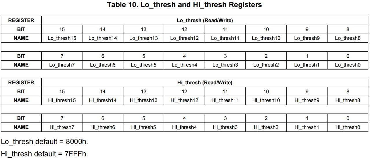
Values inside threshold registers are stored as two‑complement numbers. MSB bit‑15 equal to zero represents positive numbers; MSB equal to one represents negative numbers.
Note the effect of PGA setting: PGA modifies full‑scale input‑voltage range (FSR), which can vary from ±6.144 V down to ±0.256 V. Changing PGA gain also changes LSB voltage weight, so threshold register values must be recalculated after modifying PGA configuration.
Examples: ‑ PGA set for ±6.144 V full‑scale: 1 LSB ≈ 187.5 µV ‑ PGA set for ±0.256 V full‑scale: 1 LSB ≈ 7.8125 µV
The ALERT/RDY pin supports two functions controlled by register bits.
Alarm‑comparator function: ALERT/RDY triggers whenever conversion result goes outside the Lo_thresh / Hi_thresh window.
Data‑ready (RDY) function: In single‑shot mode ALERT/RDY reflects OS bit status after each completed conversion. In continuous‑conversion mode it pulses at conversion‑complete events. To enable RDY‑signal mode, set Hi_thresh MSB = 1 and Lo_thresh MSB = 0.
- ADS1115 I2C Communication Interface
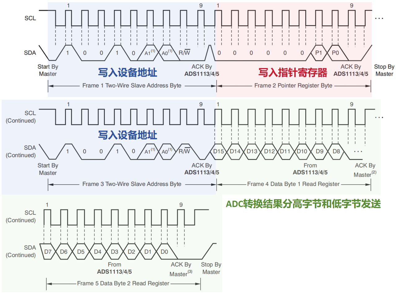
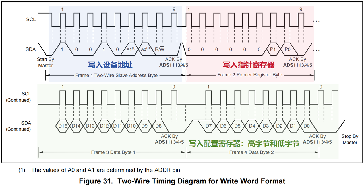
Example procedure configuring ADS1115 into continuous‑conversion mode, I²C slave address = 0x48. Write configuration values to configuration register.
- First byte: send I²C slave address
0b1001000(0x48) plus write bit0. - Second byte: write pointer‑register value
0b00000001(0x01) to point to configuration register.
- Third byte: high byte (MSB) of configuration register, example
0b10000100(0x84). This byte sets major operating‑mode parameters.
- Fourth byte: low byte (LSB) of configuration register, example
0b10000011(0x83). Contains PGA gain and data‑rate settings.
I²C write transaction format for pointer‑register and configuration‑register writes:
After configuration, read conversion results: First, set pointer register to point at conversion register.
- First byte: send slave address
0b1001000(0x48) plus write bit0. - Second byte: write pointer‑register value
0b00000000(0x00) selecting conversion register.
Then execute read sequence:
- First byte: send slave address
0b1001000plus read bit1→0b10010001. - Second byte: ADS1113/4/5 transmits high byte MSB of conversion result.
- Third byte: ADS1113/4/5 transmits low byte LSB of conversion result.
Read‑back sequence diagram for ADC conversion result: