This article introduces RP2040 GPIO pins, pin multiplexing function selection, external interrupts and configurable electrical parameters of IO pads.
COMPONENTS
PROJECT DESCRIPTION
【Preliminary Note】The original hardware example in this article was written based on the RP2040. The actual hardware used in this hands-on demonstration features the W55RP20 as the main controller chip. The circuit logic and UF2 flashing operation principles are universally applicable, with only the main controller model differing. The original chip model mentioned in the circuit descriptions below is provided for reference purposes only.
The RP2040 features 36 multi-function general-purpose input/output pins, which are divided into two groups:
QSPI Group: A total of 6 pins, namely QSPI_SS, QSPI_SCLK, and QSPI_SD0 to QSPI_SD3 (responsible for connecting to external Flash; normally acting as a "dedicated socket" for reading programs stored in Flash);
User Group (GPIO0 to GPIO29): This is the "universal interface" we commonly use in programming, which can be connected to a wide range of devices. Notably, GPIO26 to GPIO29 additionally support "analog input", making them compatible with devices that output analog signals such as temperature sensors and potentiometers.
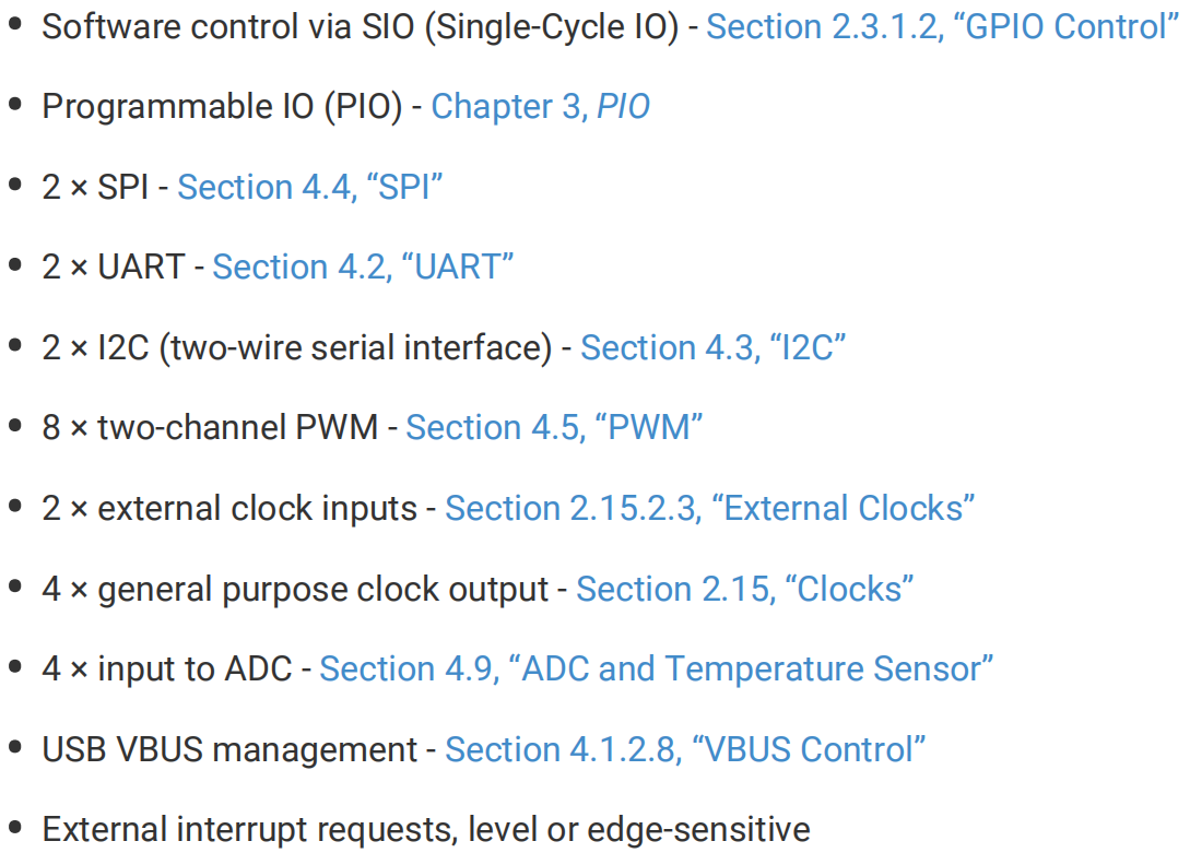
Each GPIO can be directly controlled by software running on the processor or by many other functional blocks.
1. Function Selection
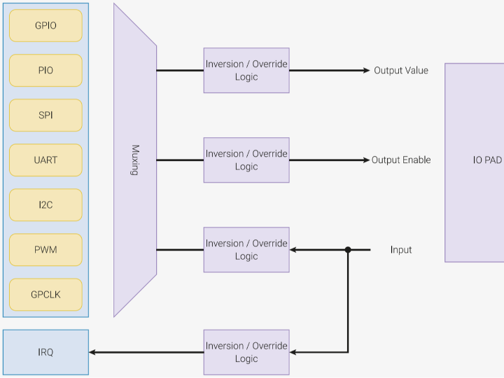
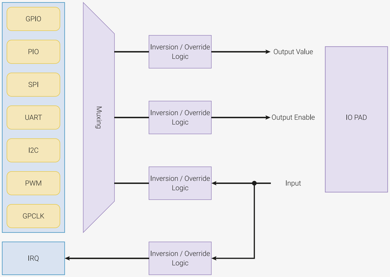
The logical structure of an example IO is shown in the following figure:
Figure 2.40 Logic Architecture Diagram of GPIO Function Selection for RP2040 Chip: Modules such as PIO and SPI on the left are selected one by one via the "function selector", and after signal inversion/forced logic processing, the signal is either output to the pin or received from the pin input, which can also trigger an interrupt.
Each GPIO can be controlled by one of multiple peripherals (meaning each GPIO pin can be switched to different functions), or by the software control registers in the SIO:
You can use the "FUNCSEL" function switch (by writing to the GPIO CTRL register) to select the function of the current pin (for example, configure GPIO0 as the receive pin of SPI0);
The signal of the pin can also be "inverted"(for example, if it originally outputs a high level, it will become a low level after inversion), or forcibly set to a fixed high or low level;
Note: Only one function can be selected for a single pin at a time, and one peripheral (such as the receiver of UART0) can only be connected to one pin — just like "only one appliance can be plugged into a single socket at a time, and one appliance can only be plugged into one socket".
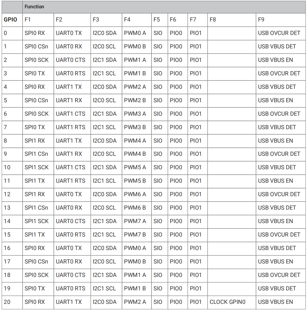
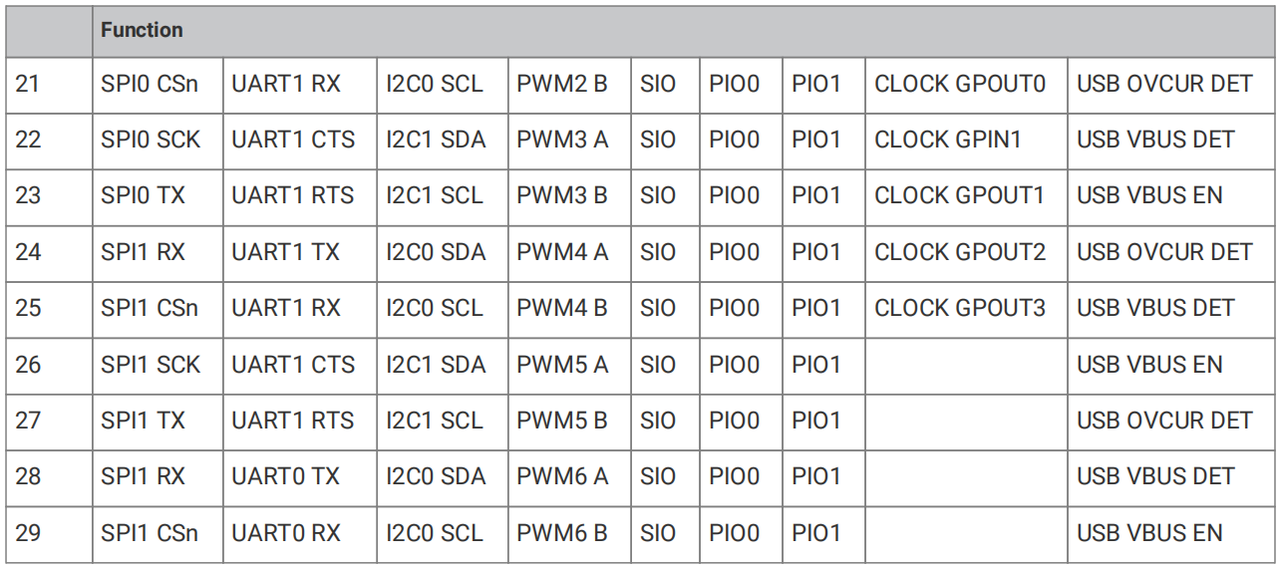
The function assigned to each GPIO is selected by writing to the FUNCSEL field in the GPIO's CTRL register. Taking GPIO0_CTRL as an example, the available functions on each IO are shown in the table below:
Figure 2.41 GPIO Function to reuse Control Diagram of RP2040 Chip (0-20)
Figure 2.42 GPIO Function Multiplexing Control Diagram of RP2040 Chip (21-29)
Each GPIO can select one function at a time. Similarly, each peripheral input (e. g., UART0 RX) can only be selected on a single GPIO at a time. If the same peripheral input is connected to multiple GPIOs, the peripheral input will see the logical OR of these GPIO inputs.
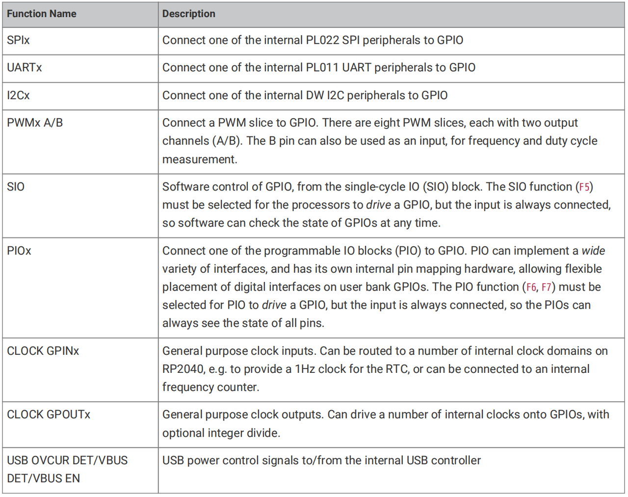
The function description of the GPIO bank is as follows:
Figure 2.43 Functional Diagram of GPIO Bank
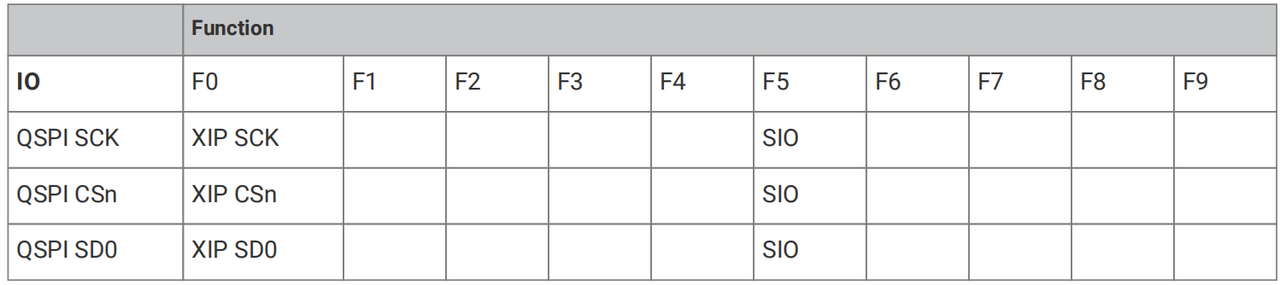
The functions of the General Purpose Input/Output (GPIO) QSPI bank are described as follows:
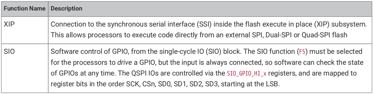
This is the QSPI pin group function option table for the RP2040, which lists the available functions for the 6 pins including QSPI_SCK, QSPI_CSn, and QSPI_SD0 to SD3: each pin is configured by default for the "XIP" function (used to connect an external Flash to enable direct program execution from Flash), and all of them support the "SIO" function, which can be switched to general GPIO under software control.
The functions of the GPIO QSPI bank are described as follows:
Figure 2.46 Functional configuration diagram of GPIO QSPI bank: "XIP" refers to the synchronous serial interface connected to external Flash, which enables the chip to execute programs directly from SPI / Dual-SPI / Quad-SPI Flash; "SIO" is the function of software-controlled GPIO. After selecting this function, these pins can be controlled through dedicated registers, and the status of the pins can be read at any time.
The six QSPI Bank GPIO pins are typically used by the XIP peripheral to communicate with external flash devices. However, there are two scenarios where these pins can be used as software-controlled GPIOs:
If the external Flash operates in "SPI / Dual SPI" mode, the SD2 and SD3 pins are not in use and can function as general-purpose GPIO pins.
If the chip does not use Flash (and only boots via USB), all these 6 pins can be used as regular GPIOs.
2. Interrupt
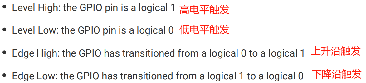
GPIO external interrupts can be configured into the following four types, and the interrupt type can be modified at any time:
Figure 2.47 Description of GPIO Interrupt and Pad Structure
3.Pads
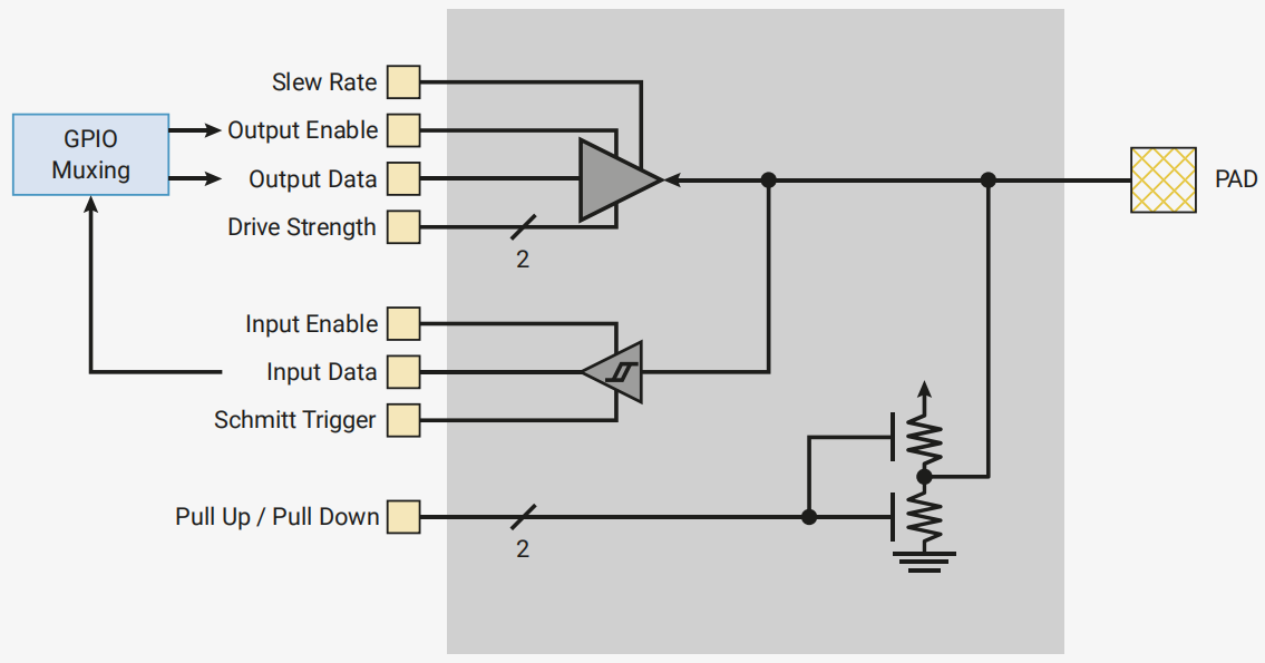
Each GPIO is connected to the outside of the chip via a "Pad". Pads serve as the electrical interface between the internal logic of the chip and external circuits, converting signal voltage levels, supporting higher currents, and providing protection against electrostatic discharge (ESD) events.
Figure 2.48 Electrical Characteristics and Structural Block Diagram of GPIO Pad
The electrical characteristics of Pads can be adjusted to adapt to external circuits, and the following adjustments are available:
Drive strength: Adjust the current that the pin can output (for example, 8mA is required to light up an LED, while only 2mA is needed to connect a sensitive sensor);
Slew Rate: Adjusts the speed of signal change on the pin (use "Fast" when connecting to high-speed devices, and "Slow" for low-speed devices for better stability);
Pull-up / Pull-down: When the pin is not connected to any device, it will automatically maintain a high or low level (to prevent the pin from "floating randomly" and causing false triggering of the device);
Schmitt trigger: Makes input signals more "interference-resistant"(for example, even if an external signal has minor fluctuations, it can still be stably recognized as a high/low level);
Disable input buffer: Turning off "signal reception" when the pin is not in use can save power.
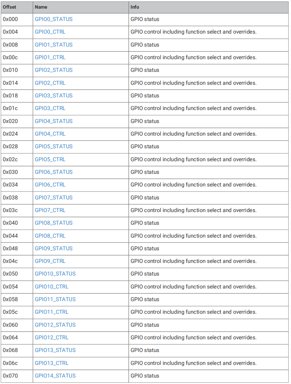
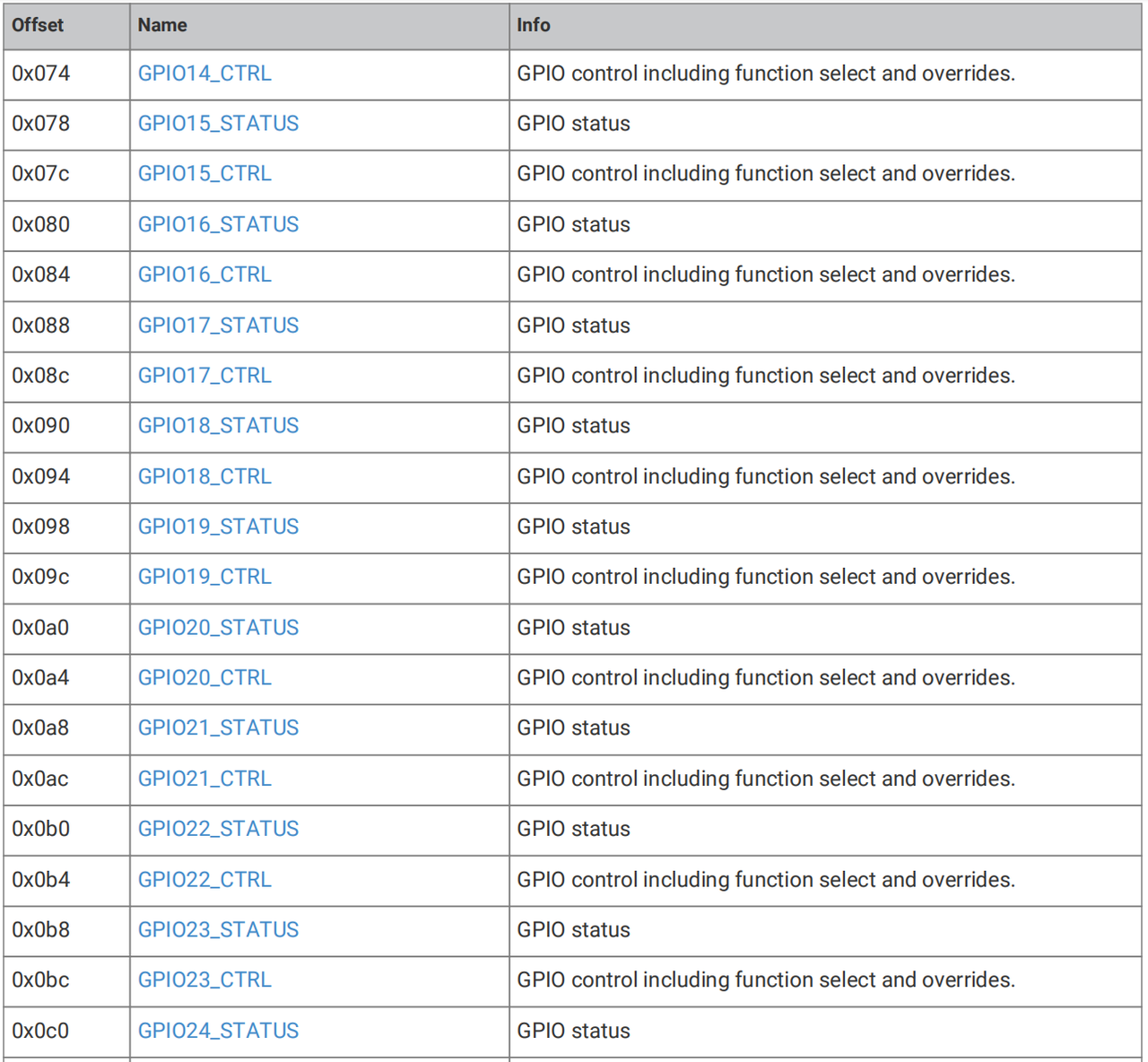
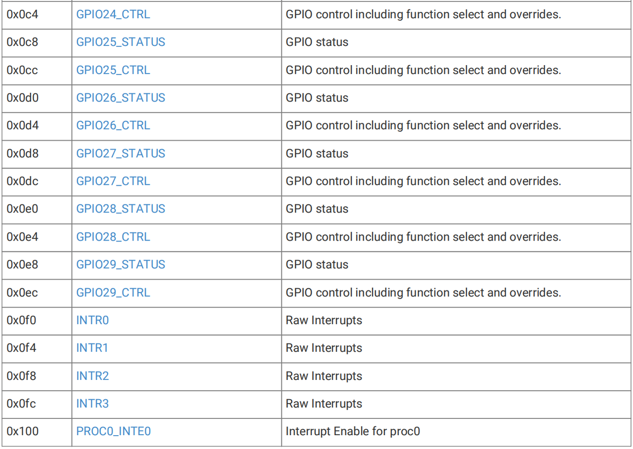
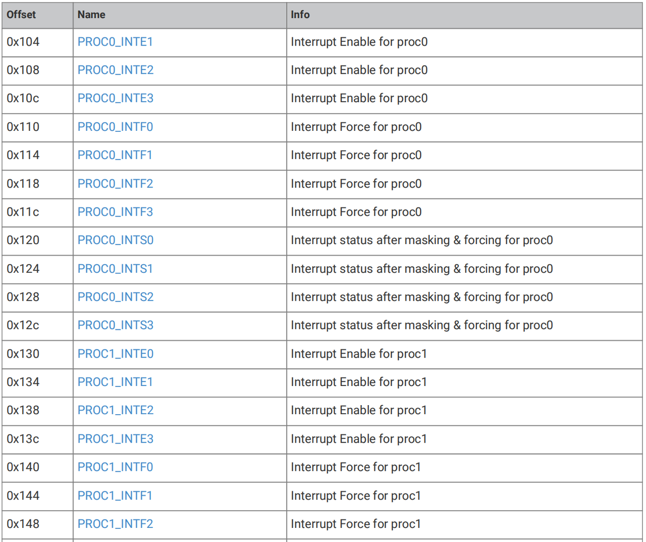
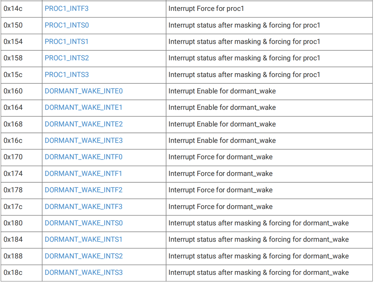
The base address of the user bank IO register is 0x40014000:
Figure 2.49 GPIO Register Address Mapping Table (GPIO0 to GPIO14)
Figure 2.50 GPIO Register Address Mapping Table (GPIO15 to GPIO24)
Figure 2.51 Interrupt Controller Register Mapping Table (Related to PROC0 and PROC1 Interrupts)
Figure 2.52 GPIO Register Address Mapping Table (Related to PROC0 and PROC1 Interrupts)
Figure 2.53 Interrupt Controller Register Mapping Table (related to PROC1 and DORMANT_WAKE interrupts)