
How to Understand W5500 Network Framing and Hardware Wiring on STM32?
This source is a hardware-and-protocol primer for the W5500 rather than a full STM32 project repository, but it is highly useful for education because it explai
How to Understand W5500 Network Framing and Hardware Wiring on STM32?
Summary
This source is a hardware-and-protocol primer for the W5500 rather than a full STM32 project repository, but it is highly useful for education because it explains both the chip’s Ethernet-side wiring and the SPI frame format that an STM32 would use to control it. In this architecture, the STM32 is the SPI host and application controller, while the W5500 is the wired Ethernet controller that exposes register space, socket register blocks, and TX/RX memory through a structured SPI transaction model.
What the Project Does
The article is not a finished end-product build. It teaches two concrete parts of W5500 integration: the hardware pin functions and the W5500 SPI frame layout. On the hardware side, it explains the Ethernet differential pairs, analog support pins, 25 MHz clock pins, SPI pins, reset and interrupt pins, PHY mode pins, and LED pins. On the protocol side, it explains that every W5500 SPI access is built from a 16-bit address field, an 8-bit control field, and an N-byte data field.
For STM32 learners, that makes the article useful as a bridge between board wiring and firmware structure. An STM32 does not talk to W5500 using a generic “Ethernet API” at first. It drives SCSn, SCLK, MOSI, and MISO, formats address and control bytes, chooses which register or memory block to access, and then reads or writes data. That layered explanation is exactly what beginners need before moving on to socket APIs or middleware.
The article also makes an important educational point about access regions. The control byte’s BSB bits select whether the STM32 is talking to the common register block, a socket register block, a socket TX buffer, or a socket RX buffer. In practice, that means STM32 firmware can use one SPI transaction model to configure the chip, inspect socket status, and move payload data in and out of the W5500 memory map.
Where WIZnet Fits
The exact WIZnet product here is the W5500. WIZnet documents describe it as a hardwired TCP/IP Ethernet controller with integrated 10/100 MAC and PHY, support for multiple hardware sockets, internal packet buffering, and an SPI host interface. The CSDN article also states that it supports TCP, UDP, IPv4, ICMP, ARP, IGMP, and PPPoE, includes eight hardware sockets, and supports SPI up to 80 MHz.
In an STM32-based design, the W5500 sits between the MCU and the Ethernet cable. The STM32 handles board initialization, GPIO control, SPI timing, and higher-level application logic. The W5500 handles Ethernet link functions, packet buffering, and socket-capable network transport. That split is what makes the chip attractive in education: students can learn embedded Ethernet without first implementing a full software TCP/IP stack on the MCU.
The article is especially useful because it does not stop at abstract block diagrams. It ties pin-level wiring and frame-level access together. That means a learner can see how an STM32 SPI transaction maps directly onto W5500 register and memory access, which is the core architectural relationship in this kind of design.
Implementation Notes
This source does use a WIZnet product, but it does not provide a full STM32 repository with file paths and line-addressable firmware. The implementation value here is architectural rather than project-specific, so I am limiting examples to what is explicitly shown in the article.
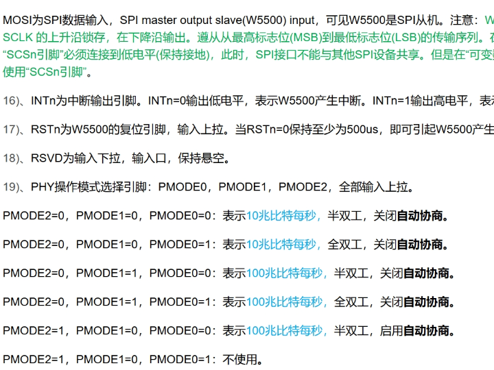
The first important implementation element is the STM32-facing hardware interface. The article identifies the SPI pins as SCSn, SCLK, MISO, and MOSI, states that W5500 supports SPI mode 0 and mode 3, and explains that data is latched on the rising edge and driven on the falling edge. It also notes that INTn is the interrupt output and that RSTn must be held low for at least 500 microseconds to trigger a hardware reset. For STM32 firmware, those are the minimum hardware rules that must be correct before any network function can work.
The second important implementation element is the SPI frame definition. The article states that a W5500 frame has three parts: a 16-bit address field, an 8-bit control field, and a data field. It further explains that the control field contains BSB bits for block selection, an RWB bit for read or write access, and OM bits for SPI operating mode. That matters because STM32 code must build the frame correctly before reading or writing any register or memory block.
The third implementation detail is the distinction between variable data length mode and fixed data length mode. The article shows macros such as _W5500_SPI_VDM_OP_, _W5500_SPI_FDM_OP_LEN1_, _W5500_SPI_FDM_OP_LEN2_, and _W5500_SPI_FDM_OP_LEN4_, and explains that VDM is controlled by the chip-select signal while FDM fixes the data length to 1, 2, or 4 bytes. For STM32 projects, that is a practical design choice: VDM is usually easier for a shared SPI bus and for general-purpose driver code, while FDM is more restrictive.
Because no STM32 project source is provided in the article, I am not inventing a board-specific code snippet. The defensible takeaway is this: wire the W5500 correctly, reset it reliably, choose SPI mode and access mode deliberately, then implement address/control/data framing before attempting higher-level socket communication.
Practical Tips / Pitfalls
- Keep TXP/TXN and RXP/RXN as matched differential pairs. Routing mistakes on the Ethernet side will cause link problems long before firmware is relevant.
- Follow the analog support-pin requirements closely. The article specifies a 12.4 kΩ resistor on EXRES1, a 4.7 µF capacitor on TOCAP, and a 10 nF capacitor on 1V2O.
- Verify reset timing early. RSTn must be held low for at least 500 µs, and weak reset handling can look like random SPI or link failures.
- Use SPI mode 0 or 3 only. The article is explicit that W5500 supports those modes, with rising-edge capture and falling-edge output.
- Prefer VDM during STM32 bring-up unless there is a specific reason to use FDM. It is easier to manage and more compatible with shared SPI buses.
- Start with common-register reads and writes before touching socket buffers. That keeps framing bugs separate from network-stack bugs. This is an inference from the article’s structure.
FAQ
Why use the W5500 on STM32 for this kind of project?
Because it gives an STM32 a wired Ethernet path with a hardware-offloaded TCP/IP model. That lets students learn SPI access, register maps, and socket concepts without implementing a full Ethernet stack entirely in MCU software.
How does the W5500 connect to the STM32?
Through SPI using SCSn, SCLK, MOSI, and MISO, plus control pins such as RSTn and optionally INTn. The article also explains the clock, PHY mode, LED, and analog support pins that must be wired correctly for a working board.
What role does the W5500 play in this specific source?
It is both the subject of the lesson and the Ethernet controller being explained. The article focuses on how an MCU such as an STM32 would access its registers, memory regions, and socket blocks through framed SPI transactions.
Can beginners follow this?
Yes, if they already know basic STM32 GPIO and SPI concepts. It is better suited to beginner-to-intermediate embedded learners than to absolute beginners, because it assumes the reader can interpret pin roles, reset timing, and communication bit fields.
How does this compare with LwIP on STM32?
LwIP gives more software flexibility, but it also moves more stack responsibility into MCU RAM, firmware integration, and debugging. The W5500 approach instead keeps Ethernet transport in dedicated hardware and exposes a register-and-socket access model over SPI. That usually makes the first learning path simpler on small MCU systems. This comparison is an inference supported by the W5500 architecture described in the sources.
Source
Original article: CSDN post, “W5500的引脚和W5500帧,” published August 5, 2025, under CC 4.0 BY-SA. Product facts were checked against WIZnet’s official W5500 datasheet.
Tags
W5500, WIZnet, STM32, SPI, Embedded Ethernet, Hardware TCP/IP, Ethernet Wiring, Register Access, Socket Offload, Education, MCU Networking, PHY Design
How to Understand W5500 Network Framing and Hardware Wiring on STM32?
Summary
This source is a hardware-and-protocol primer for the W5500 rather than a full STM32 project repository, but it is highly useful for education because it explains both the chip’s Ethernet-side wiring and the SPI frame format that an STM32 would use to control it. In this architecture, the STM32 is the SPI host and application controller, while the W5500 is the wired Ethernet controller that exposes register space, socket register blocks, and TX/RX memory through a structured SPI transaction model.
What the Project Does
The article is not a finished end-product build. It teaches two concrete parts of W5500 integration: the hardware pin functions and the W5500 SPI frame layout. On the hardware side, it explains the Ethernet differential pairs, analog support pins, 25 MHz clock pins, SPI pins, reset and interrupt pins, PHY mode pins, and LED pins. On the protocol side, it explains that every W5500 SPI access is built from a 16-bit address field, an 8-bit control field, and an N-byte data field.
For STM32 learners, that makes the article useful as a bridge between board wiring and firmware structure. An STM32 does not talk to W5500 using a generic “Ethernet API” at first. It drives SCSn, SCLK, MOSI, and MISO, formats address and control bytes, chooses which register or memory block to access, and then reads or writes data. That layered explanation is exactly what beginners need before moving on to socket APIs or middleware.
The article also makes an important educational point about access regions. The control byte’s BSB bits select whether the STM32 is talking to the common register block, a socket register block, a socket TX buffer, or a socket RX buffer. In practice, that means STM32 firmware can use one SPI transaction model to configure the chip, inspect socket status, and move payload data in and out of the W5500 memory map.
Where WIZnet Fits
The exact WIZnet product here is the W5500. WIZnet documents describe it as a hardwired TCP/IP Ethernet controller with integrated 10/100 MAC and PHY, support for multiple hardware sockets, internal packet buffering, and an SPI host interface. The CSDN article also states that it supports TCP, UDP, IPv4, ICMP, ARP, IGMP, and PPPoE, includes eight hardware sockets, and supports SPI up to 80 MHz.
In an STM32-based design, the W5500 sits between the MCU and the Ethernet cable. The STM32 handles board initialization, GPIO control, SPI timing, and higher-level application logic. The W5500 handles Ethernet link functions, packet buffering, and socket-capable network transport. That split is what makes the chip attractive in education: students can learn embedded Ethernet without first implementing a full software TCP/IP stack on the MCU.
The article is especially useful because it does not stop at abstract block diagrams. It ties pin-level wiring and frame-level access together. That means a learner can see how an STM32 SPI transaction maps directly onto W5500 register and memory access, which is the core architectural relationship in this kind of design.
Implementation Notes
This source does use a WIZnet product, but it does not provide a full STM32 repository with file paths and line-addressable firmware. The implementation value here is architectural rather than project-specific, so I am limiting examples to what is explicitly shown in the article.
The first important implementation element is the STM32-facing hardware interface. The article identifies the SPI pins as SCSn, SCLK, MISO, and MOSI, states that W5500 supports SPI mode 0 and mode 3, and explains that data is latched on the rising edge and driven on the falling edge. It also notes that INTn is the interrupt output and that RSTn must be held low for at least 500 microseconds to trigger a hardware reset. For STM32 firmware, those are the minimum hardware rules that must be correct before any network function can work.
The second important implementation element is the SPI frame definition. The article states that a W5500 frame has three parts: a 16-bit address field, an 8-bit control field, and a data field. It further explains that the control field contains BSB bits for block selection, an RWB bit for read or write access, and OM bits for SPI operating mode. That matters because STM32 code must build the frame correctly before reading or writing any register or memory block.
The third implementation detail is the distinction between variable data length mode and fixed data length mode. The article shows macros such as _W5500_SPI_VDM_OP_, _W5500_SPI_FDM_OP_LEN1_, _W5500_SPI_FDM_OP_LEN2_, and _W5500_SPI_FDM_OP_LEN4_, and explains that VDM is controlled by the chip-select signal while FDM fixes the data length to 1, 2, or 4 bytes. For STM32 projects, that is a practical design choice: VDM is usually easier for a shared SPI bus and for general-purpose driver code, while FDM is more restrictive.
Because no STM32 project source is provided in the article, I am not inventing a board-specific code snippet. The defensible takeaway is this: wire the W5500 correctly, reset it reliably, choose SPI mode and access mode deliberately, then implement address/control/data framing before attempting higher-level socket communication.
Practical Tips / Pitfalls
- Keep TXP/TXN and RXP/RXN as matched differential pairs. Routing mistakes on the Ethernet side will cause link problems long before firmware is relevant.
- Follow the analog support-pin requirements closely. The article specifies a 12.4 kΩ resistor on EXRES1, a 4.7 µF capacitor on TOCAP, and a 10 nF capacitor on 1V2O.
- Verify reset timing early. RSTn must be held low for at least 500 µs, and weak reset handling can look like random SPI or link failures.
- Use SPI mode 0 or 3 only. The article is explicit that W5500 supports those modes, with rising-edge capture and falling-edge output.
- Prefer VDM during STM32 bring-up unless there is a specific reason to use FDM. It is easier to manage and more compatible with shared SPI buses.
- Start with common-register reads and writes before touching socket buffers. That keeps framing bugs separate from network-stack bugs. This is an inference from the article’s structure.
FAQ
Why use the W5500 on STM32 for this kind of project?
Because it gives an STM32 a wired Ethernet path with a hardware-offloaded TCP/IP model. That lets students learn SPI access, register maps, and socket concepts without implementing a full Ethernet stack entirely in MCU software.
How does the W5500 connect to the STM32?
Through SPI using SCSn, SCLK, MOSI, and MISO, plus control pins such as RSTn and optionally INTn. The article also explains the clock, PHY mode, LED, and analog support pins that must be wired correctly for a working board.
What role does the W5500 play in this specific source?
It is both the subject of the lesson and the Ethernet controller being explained. The article focuses on how an MCU such as an STM32 would access its registers, memory regions, and socket blocks through framed SPI transactions.
Can beginners follow this?
Yes, if they already know basic STM32 GPIO and SPI concepts. It is better suited to beginner-to-intermediate embedded learners than to absolute beginners, because it assumes the reader can interpret pin roles, reset timing, and communication bit fields.
How does this compare with LwIP on STM32?
LwIP gives more software flexibility, but it also moves more stack responsibility into MCU RAM, firmware integration, and debugging. The W5500 approach instead keeps Ethernet transport in dedicated hardware and exposes a register-and-socket access model over SPI. That usually makes the first learning path simpler on small MCU systems. This comparison is an inference supported by the W5500 architecture described in the sources.
Source
Original article: CSDN post, “W5500的引脚和W5500帧,” published August 5, 2025, under CC 4.0 BY-SA. Product facts were checked against WIZnet’s official W5500 datasheet.
Tags
W5500, WIZnet, STM32, SPI, Embedded Ethernet, Hardware TCP/IP, Ethernet Wiring, Register Access, Socket Offload, Education, MCU Networking, PHY Design