



How to Build TCP Networking with W5500 on a Zynq FPGA?
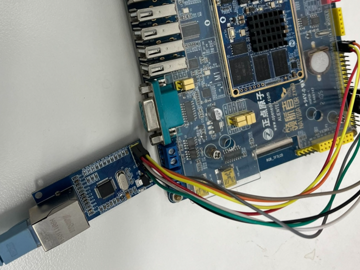
This project connects FPGA logic on a Zynq platform directly to a Windows TCP application using the WIZnet W5500 over SPI.
How to Build TCP Networking with W5500 on a Zynq FPGA?
Summary
This project connects FPGA logic on a Zynq platform directly to a Windows TCP application using the WIZnet W5500 over SPI. The FPGA implements the SPI controller, socket-control state machines, buffering, and data-path logic in Verilog, while the W5500 handles Ethernet MAC/PHY functions and the hardwired TCP/IP stack. The result is a useful educational architecture for studying where hardware networking offload ends and FPGA application logic begins.
What the Project Does
The source project uses a Zynq expansion interface and Vivado 2019.2, with the networking control written as portable Verilog rather than relying on a processor-side networking library. Its stated goal is to let the FPGA communicate directly with a Windows host through TCP. The demonstrated configuration currently implements one W5500 socket, although the Verilog architecture is intended to be extended to multiple sockets.
The data path is essentially:
Windows TCP application → Ethernet → W5500 → SPI → FPGA receive logic → buffer/processing → SPI → W5500 → Ethernet → Windows
For testing, the author sends TCP data from a PC at approximately 10 ms intervals while simultaneously running ping. The FPGA receives the TCP payload, buffers it, and returns it as an internal loopback. The article reports no packet loss under that test and also reports a 24-hour stress run without observed bit errors; however, no downloadable repository, raw test log, or reproducible benchmark package is linked in the article, so these should be treated as author-reported measurements rather than independently verified performance figures.
From an educational perspective, this arrangement exposes several useful FPGA networking concepts at once: SPI timing, finite-state-machine design, clock-domain handling, buffering, interrupt processing, socket state management, and the boundary between an application datapath and an offloaded TCP/IP implementation.
Where WIZnet Fits
The WIZnet W5500 is the network processor between the FPGA fabric and the Ethernet cable. It contains a hardwired TCP/IP engine, 10/100 Ethernet MAC and PHY, eight hardware sockets, and 32 KB of internal TX/RX memory. The host accesses its registers and socket buffers through SPI; the device supports SPI Mode 0 and Mode 3 and an SPI clock of up to 80 MHz according to the W5500 datasheet.
That distinction is important for an FPGA implementation. The Verilog does not need to implement TCP congestion control, retransmission, ARP processing, TCP state transitions, or an Ethernet MAC in programmable logic. Instead, the FPGA controls W5500 socket registers, transfers payload data to and from the W5500 buffers, and responds to network events. W5500 handles TCP, UDP, IPv4, ICMP, ARP, IGMP, and related Ethernet processing internally.
The host interface also maps naturally onto FPGA logic. W5500 uses four main SPI signals—SCSn, SCLK, MOSI, and MISO—and operates as the SPI slave. Each transaction contains a 16-bit offset address, an 8-bit control field, and a data phase. The control field selects the common registers, one of the socket register blocks, or the associated TX/RX memory. This makes a deterministic state-machine-based master practical without requiring a software execution environment.
The article specifically uses about 30 MHz SPI, which is an implementation choice rather than the W5500 limit. WIZnet specifies support up to 80 MHz, while the article's author reports that 30 MHz was the stable operating point on the tested PCB and FPGA configuration. This difference is useful in an educational setting because it demonstrates that device maximum ratings and achievable board-level timing margin are not the same thing.
W5500 versus a software TCP/IP stack
A software stack such as lwIP takes a different architectural approach. lwIP implements TCP/IP in software and is intended for embedded systems with limited RAM. Its raw API can operate without an operating system, but the TCP/IP code still executes on a processor. On an FPGA platform, that normally means using the Zynq processing system or adding a soft CPU and connecting that software stack to an Ethernet MAC driver.
With W5500, the TCP/IP execution moves into the external Ethernet controller. The FPGA can therefore remain primarily an RTL design and interact with network connections as W5500 sockets rather than executing a C networking stack. This is particularly useful for teaching FPGA state machines and hardware datapaths without first requiring an RTOS, soft-core processor, Ethernet MAC driver, and TCP/IP software port.
The trade-off is flexibility. lwIP provides a software-controlled TCP/IP implementation including IPv4 and IPv6 and allows developers to modify configuration, memory management, APIs, and protocol behavior. The W5500 provides a fixed hardwired IPv4 networking engine and a defined socket/register model. For an educational FPGA exercise focused on RTL-to-Ethernet communication, the W5500 substantially reduces the amount of networking logic that must be built before useful TCP traffic can be exchanged.
Implementation Notes
The source is a CSDN technical article rather than a linked source repository. It contains several real Verilog excerpts, but it does not provide filenames or repository paths. The locations below therefore refer to the inline excerpts in the original article rather than invented source files.
SPI state-machine control
Source location: CSDN article, inline Verilog excerpt around lines 28–41.
parameter SPI_IDLE  = 3'd0;
parameter SPI_START = 3'd2;

spi_cs_n = 1'b0;
This logic is part of the FPGA-side SPI finite-state machine. The state machine controls when the W5500 is selected and coordinates the SPI clock edges around each transaction. The article states that a counter-generated SPI waveform was used so timing could be adjusted directly in RTL.
That structure matches the W5500 host interface well because SCSn defines transaction boundaries in variable-length mode. W5500 samples data on the rising edge of SCLK and changes output data on the falling edge in both supported SPI modes. Correct CS and clock sequencing is therefore a functional part of the network interface, not simply a peripheral detail.
Receive buffering and TCP loopback
Source location: CSDN article, inline Verilog excerpt around lines 47–57.
reg [7:0] rx_buffer[0:2047];

if(tx_trigger)
    tx_data <= rx_buffer[rd_ptr];
The buffer decouples incoming W5500 data from the transmit datapath. After TCP data is retrieved from the W5500 receive side, the FPGA stores it locally and reads it back when the transmit logic is ready. This is the mechanism used for the article's TCP loopback test.
The article also describes separate receive/transmit timing domains and interrupt-driven data movement. These are relevant FPGA design issues even though TCP itself runs inside W5500: hardware offload removes the protocol implementation, but the FPGA still has to manage buffering, socket events, SPI bandwidth, and clock-domain boundaries correctly.
One terminology point in the original source needs clarification. The article describes a 1460-byte FIFO as matching the default “MTU.” In a conventional Ethernet/IPv4/TCP configuration, 1500 bytes is the usual Ethernet IP MTU, while 1460 bytes corresponds to a common TCP maximum segment payload after the normal IPv4 and TCP headers. The 1460-byte buffer choice can therefore make sense for TCP payload handling, but it should not be interpreted as the Ethernet MTU itself.
Practical Tips / Pitfalls
Start below the maximum SPI clock. W5500 supports SPI clocks up to 80 MHz, but the source design reports using 30 MHz for its tested PCB. Establish correct register access at a conservative clock first, then increase the rate while checking timing margin and signal integrity.
Implement the W5500 SPI frame explicitly. The FPGA must generate the 16-bit address phase, control byte, and data phase correctly. The block-select bits determine whether the transaction accesses common registers, socket registers, TX memory, or RX memory.
Treat SCSn timing as part of the protocol. The source reports that an unstable CS signal caused severe receive problems during early testing. Use registered outputs and verify SCLK, MOSI, MISO, and SCSn with an oscilloscope or logic analyzer.
Do not copy the article's RC modification blindly. The author reports adding a 20 Ω resistor and 100 pF capacitor while debugging the particular board. Component values for edge-rate or ringing control depend on driver impedance, trace geometry, loading, and topology; validate the actual waveform on your own PCB before adding filtering.
Design buffering around the application datapath, not just TCP. W5500 has 32 KB of internal socket memory, but FPGA-side FIFOs may still be required to absorb SPI latency, clock-domain differences, and bursty application data.
Bring up one socket first. The original project currently demonstrates one socket even though W5500 supports eight. A useful progression is SPI register access → PHY/link check → network configuration → one TCP socket → verified TX/RX → additional sockets.
Separate W5500 limits from FPGA limits. Socket count and internal network buffering are W5500 resources, while RTL state machines, local FIFOs, clock crossings, and SPI scheduling consume FPGA resources. Scaling to multiple sockets requires managing both sides rather than only changing a Verilog parameter.
FAQ
Q: Why use the W5500 for TCP networking on an FPGA?
A: W5500 executes TCP/IP, MAC, and PHY functions in hardware and exposes network connections through socket registers and TX/RX buffers. That allows an FPGA to reach Ethernet through an SPI state machine without implementing TCP in RTL or running a software TCP/IP stack on a processor. It also provides eight hardware sockets and 32 KB of internal network buffer memory.
Q: How does the W5500 connect to the FPGA?
A: The FPGA acts as the SPI master and the W5500 as the SPI slave using SCSn, SCLK, MOSI, and MISO; INTn and RSTn can additionally be used for interrupt handling and reset. W5500 supports SPI Mode 0 and Mode 3, with each access carrying a 16-bit register/buffer address, an 8-bit control field, and the payload data.
Q: What exactly does the W5500 do in this project?
A: It forms the Ethernet and TCP endpoint between the Verilog datapath and the Windows TCP application. The FPGA manages SPI transactions, W5500 socket state, local buffering, and loopback data movement, while W5500 processes the actual Ethernet and TCP/IP protocols and stores network data in its socket buffers.
Q: Can beginners use this project to learn FPGA Ethernet networking?
A: It is suitable as an intermediate educational project rather than a first Verilog exercise. A learner should already understand finite-state machines, synchronous design, SPI, counters, basic clock-domain concepts, IPv4 addressing, and TCP client/server behavior. The advantage of W5500 is that students can study the FPGA-to-network boundary without first implementing an Ethernet MAC and TCP/IP stack themselves.
Q: How does W5500 compare with lwIP on an FPGA platform?
A: W5500 performs TCP/IP processing in dedicated hardware and lets FPGA logic manipulate sockets over SPI. lwIP is a software TCP/IP implementation that executes on a processor and provides raw, sequential, and socket-style APIs; on an FPGA system this normally places networking on a hard or soft CPU rather than directly in pure RTL. lwIP offers greater protocol and software flexibility, including IPv6 support, while W5500 simplifies a pure-Verilog TCP design by moving the IPv4 TCP/IP stack outside the FPGA.
Source
Original Project: CSDN article, “当FPGA老司机遇上W5500:TCP通信的硬核调教实录”. The page describes a Zynq/W5500 TCP test platform using Vivado 2019.2 and portable Verilog. The article is published under CC BY-SA 4.0. No actual GitHub repository is linked; the article explicitly contains a placeholder reference rather than a repository URL.
WIZnet Technical Reference: W5500 Datasheet Version 1.1.0, covering the hardwired TCP/IP architecture, eight sockets, 32 KB TX/RX memory, SPI interface, socket register mapping, and SPI timing.
Software-stack comparison: Official lwIP documentation describing the raw TCP/IP API and the lightweight software-stack architecture.
Tags
#W5500 #FPGA #Zynq #Verilog #TCP #Ethernet #SPI #HardwareTCPIP #lwIP #Education
Zynq FPGA에서 W5500으로 TCP 네트워킹을 구현하는 방법은?
Summary
이 프로젝트는 Zynq 플랫폼의 FPGA 로직과 Windows TCP 애플리케이션을 WIZnet W5500과 SPI를 통해 직접 연결합니다. FPGA는 Verilog로 SPI 컨트롤러, 소켓 제어 상태 머신, 버퍼링, 데이터 경로를 구현하고, W5500은 Ethernet MAC/PHY와 하드웨어 TCP/IP 스택을 담당합니다. 따라서 FPGA 애플리케이션 로직과 하드웨어 네트워크 오프로딩의 경계를 학습하기에 적합한 교육용 구조입니다.
What the Project Does
원본 프로젝트는 Zynq 확장 인터페이스와 Vivado 2019.2를 사용하며, 프로세서 측 네트워크 라이브러리에 의존하지 않고 네트워크 제어 로직을 이식 가능한 Verilog로 구현합니다. 목표는 FPGA가 Windows 호스트와 TCP로 직접 통신하도록 만드는 것입니다. 현재 예제에서는 W5500 소켓 하나를 사용하지만, Verilog 구조 자체는 여러 소켓으로 확장할 수 있도록 설계되어 있습니다.
데이터 흐름은 다음과 같습니다.
Windows TCP 애플리케이션 → Ethernet → W5500 → SPI → FPGA 수신 로직 → 버퍼/처리 → SPI → W5500 → Ethernet → Windows
테스트에서는 PC가 약 10 ms 간격으로 TCP 데이터를 전송하면서 동시에 ping을 수행합니다. FPGA는 TCP 페이로드를 수신해 내부 버퍼에 저장한 뒤 다시 전송하는 루프백 동작을 수행합니다.
원문 작성자는 해당 조건에서 패킷 손실이 없었으며, 24시간 스트레스 테스트에서도 비트 오류를 발견하지 못했다고 설명합니다. 다만 다운로드 가능한 저장소, 원시 테스트 로그, 재현 가능한 벤치마크 자료가 제공되지 않으므로 이 수치는 독립적으로 검증된 성능 결과가 아니라 원문 작성자의 테스트 결과로 보는 것이 적절합니다.
교육 관점에서는 한 프로젝트에서 다음 FPGA 네트워크 설계 요소를 함께 다룰 수 있다는 점이 의미 있습니다.
- SPI 타이밍
- 유한 상태 머신
- 클럭 도메인 처리
- 데이터 버퍼링
- 인터럽트 처리
- 소켓 상태 관리
- FPGA 애플리케이션 데이터 경로와 TCP/IP 오프로딩의 역할 분리
Where WIZnet Fits
이 프로젝트에서 WIZnet W5500은 FPGA 패브릭과 Ethernet 케이블 사이의 네트워크 프로세서 역할을 합니다.
W5500에는 하드웨어 TCP/IP 엔진, 10/100 Ethernet MAC/PHY, 8개의 하드웨어 소켓, 총 32 KB의 내부 TX/RX 메모리가 포함되어 있습니다. FPGA는 SPI를 통해 W5500의 레지스터와 소켓 버퍼를 제어합니다. W5500은 SPI Mode 0과 Mode 3을 지원하며, 데이터시트 기준 SPI 클럭은 최대 80 MHz까지 지원합니다.
이 구조에서 중요한 점은 FPGA가 TCP 프로토콜 자체를 구현하지 않는다는 것입니다.
FPGA 로직에서 직접 구현할 필요가 없는 항목은 다음과 같습니다.
- TCP 재전송
- TCP 연결 상태 처리
- ARP 처리
- Ethernet MAC
- TCP/IP 프로토콜 처리
대신 FPGA는 W5500의 소켓 레지스터를 설정하고, TX/RX 버퍼에 데이터를 읽고 쓰며, 네트워크 이벤트를 처리합니다. 실제 TCP, UDP, IPv4, ICMP, ARP, IGMP 등의 처리는 W5500 내부에서 수행됩니다.
FPGA와의 연결도 비교적 단순합니다.
W5500의 주요 SPI 신호는 다음 네 개입니다.
- SCSn
- SCLK
- MOSI
- MISO
FPGA가 SPI Master, W5500이 SPI Slave로 동작합니다.
각 SPI 접근은 기본적으로 다음 구조를 가집니다.
16-bit Offset Address → 8-bit Control Field → Data
Control Field를 통해 Common Register, Socket Register, Socket TX Memory, Socket RX Memory 중 어느 영역을 접근할지 결정합니다.
이 구조는 소프트웨어 기반 드라이버뿐 아니라 FPGA 상태 머신으로도 구현하기 쉽습니다.
원문에서는 약 30 MHz SPI 클럭을 사용합니다. 이는 W5500 자체의 최대 속도가 아니라 해당 FPGA와 PCB 환경에서 작성자가 안정적으로 사용한 설정입니다. W5500 데이터시트의 최대 SPI 클럭은 80 MHz입니다.
교육용 프로젝트에서는 이 차이도 중요한 학습 요소입니다. 칩의 최대 사양과 실제 PCB에서 확보되는 타이밍 마진은 동일하지 않기 때문입니다.
W5500과 소프트웨어 TCP/IP 스택 비교
lwIP와 같은 소프트웨어 TCP/IP 스택은 구조가 다릅니다.
lwIP는 TCP/IP 처리를 소프트웨어로 수행합니다. 운영체제가 없는 환경에서도 Raw API를 사용할 수 있지만, 결국 TCP/IP 코드는 CPU에서 실행되어야 합니다.
따라서 Zynq 또는 다른 FPGA 플랫폼에서 lwIP를 사용하려면 일반적으로 다음과 같은 구조가 필요합니다.
Ethernet PHY → Ethernet MAC → CPU → lwIP → Application
CPU는 Zynq의 ARM Processing System일 수도 있고 FPGA 내부의 Soft CPU일 수도 있습니다.
반면 W5500을 사용하면 구조가 다음처럼 바뀝니다.
Ethernet → W5500 TCP/IP Engine → SPI → FPGA RTL
TCP/IP 실행을 외부 Ethernet 컨트롤러로 이동시키기 때문에 FPGA는 소켓과 페이로드 중심으로 네트워크를 처리할 수 있습니다.
이는 교육용 FPGA 프로젝트에서 특히 유용합니다. TCP 통신을 실습하기 위해 먼저 RTOS, Soft CPU, Ethernet MAC Driver, TCP/IP Software Port까지 준비할 필요가 없기 때문입니다.
대신 유연성 측면에서는 lwIP가 유리합니다. lwIP는 소프트웨어이므로 프로토콜 구성, 메모리 관리, API, 네트워크 동작 등을 개발자가 더 세밀하게 제어할 수 있으며 IPv6도 지원합니다.
W5500은 고정된 하드웨어 IPv4 TCP/IP 엔진과 Socket/Register 모델을 사용합니다.
따라서 FPGA RTL 중심의 TCP 교육에서는 W5500이 구조를 단순화하고, 네트워크 프로토콜을 깊게 수정해야 하는 시스템에서는 lwIP 같은 소프트웨어 스택이 더 유연합니다.
Implementation Notes
원본 자료는 GitHub 저장소가 아니라 CSDN 기술 블로그입니다. 실제 Verilog 코드 일부는 포함되어 있지만 파일명이나 저장소 경로는 제공되지 않습니다. 따라서 아래 위치 정보는 실제 파일 경로가 아니라 원문에 포함된 코드 위치를 기준으로 설명합니다.
SPI 상태 머신 제어
Source location: CSDN 원문 내 SPI 관련 Verilog 코드 부분
이 코드는 FPGA 측 SPI 상태 머신의 일부입니다.
상태 머신은 W5500의 Chip Select를 제어하고 SPI Transaction의 시작과 종료, 클럭 타이밍을 관리합니다. 원문에서는 카운터를 기반으로 SPI 파형을 생성하여 RTL에서 직접 타이밍을 조절하는 방식을 사용합니다.
W5500에서는 SCSn이 SPI Transaction의 경계를 결정하기 때문에 CS 제어는 단순한 GPIO 제어 이상의 의미를 가집니다.
W5500은 지원되는 SPI 모드에서 SCLK 상승 에지에 입력 데이터를 샘플링하고, 하강 에지에 출력 데이터를 변경합니다. 따라서 SCLK와 CS의 관계가 잘못되면 레지스터 접근과 데이터 송수신이 모두 불안정해질 수 있습니다.
수신 버퍼와 TCP Loopback
Source location: CSDN 원문 내 RX Buffer 관련 Verilog 코드 부분
이 버퍼는 W5500에서 수신한 데이터와 FPGA의 송신 데이터 경로를 분리합니다.
TCP 데이터를 W5500에서 읽은 뒤 FPGA 내부 메모리에 저장하고, 송신 로직이 준비되면 다시 데이터를 읽어 W5500으로 전송합니다.
원문의 TCP Loopback 테스트가 이 구조를 사용합니다.
TCP 프로토콜 자체는 W5500이 처리하지만 FPGA 설계에서는 여전히 다음 문제를 처리해야 합니다.
- SPI 처리 지연
- RX/TX 버퍼링
- 클럭 도메인 간 데이터 전달
- Socket Interrupt
- Socket State
- SPI Bandwidth
- Application Data Flow
즉, TCP/IP 오프로딩이 FPGA 설계를 단순화하기는 하지만 FPGA 측 데이터 경로 설계까지 없어지는 것은 아닙니다.
원문의 용어 중 하나는 구분해서 이해할 필요가 있습니다. 작성자는 약 1460-byte 크기의 FIFO를 기본 “MTU”와 연결해 설명하지만, 일반적인 Ethernet/IPv4/TCP 환경에서 Ethernet IP MTU는 1500 bytes이고, 1460 bytes는 일반적인 IPv4/TCP 헤더를 제외한 TCP 최대 Payload 크기에 해당합니다.
따라서 TCP Payload를 기준으로 1460-byte 버퍼를 구성하는 것은 합리적일 수 있지만, 1460 bytes 자체를 Ethernet MTU라고 보는 것은 정확하지 않습니다.
Practical Tips / Pitfalls
- 처음부터 최대 SPI 속도로 동작시키지 않는 것이 좋습니다. W5500은 최대 80 MHz SPI를 지원하지만, 원본 프로젝트에서는 약 30 MHz를 사용했습니다. 낮은 클럭에서 레지스터 접근과 송수신을 먼저 검증한 뒤 속도를 높이는 편이 안정적입니다.
- W5500 SPI Frame을 명확하게 구현해야 합니다. FPGA는 16-bit Address, Control Byte, Data Phase를 정확히 생성해야 하며, Block Select 설정에 따라 Common Register, Socket Register, TX/RX Memory 접근 대상이 달라집니다.
- SCSn 타이밍을 중요하게 다뤄야 합니다. 원문에서는 불안정한 CS 신호가 수신 오류의 주요 원인 중 하나였다고 설명합니다. Logic Analyzer나 Oscilloscope로 SCLK, MOSI, MISO, SCSn을 함께 확인하는 것이 좋습니다.
- 원문에서 사용한 RC 값을 그대로 복사해서는 안 됩니다. 작성자는 특정 PCB에서 20 Ω 저항과 100 pF 커패시터를 추가했다고 설명하지만, 적절한 값은 Trace 길이, Driver Impedance, Load, PCB 구조에 따라 달라집니다.
- W5500 내부 버퍼가 있어도 FPGA 측 FIFO가 필요할 수 있습니다. W5500은 내부 Socket Memory를 제공하지만 SPI 지연, Application Burst, Clock Domain 차이를 흡수하려면 FPGA 내부 Buffer가 여전히 필요합니다.
- 한 개의 Socket부터 검증하는 것이 좋습니다. SPI Register Access → PHY Link 확인 → IP 설정 → TCP Socket 하나 → TX/RX 확인 → Multi-Socket 순서로 확장하면 디버깅이 쉽습니다.
- W5500 자원과 FPGA 자원을 구분해서 설계해야 합니다. Socket 개수와 내부 Network Buffer는 W5500 자원이고, FSM, FIFO, CDC, SPI Scheduler는 FPGA 자원입니다. Multi-Socket 확장 시 양쪽을 모두 고려해야 합니다.
FAQ
Q: FPGA TCP 네트워킹에서 왜 W5500을 사용하나요?
A: W5500은 TCP/IP, Ethernet MAC, PHY 처리를 하드웨어로 수행하고 FPGA에는 Socket Register와 TX/RX Buffer 인터페이스를 제공합니다. 따라서 FPGA에서 TCP를 직접 구현하거나 CPU에서 소프트웨어 TCP/IP 스택을 실행하지 않고도 Ethernet TCP 통신을 구현할 수 있습니다. W5500은 8개의 하드웨어 소켓과 총 32 KB의 내부 TX/RX 메모리를 제공합니다.
Q: W5500은 FPGA와 어떻게 연결하나요?
A: FPGA가 SPI Master, W5500이 SPI Slave로 연결됩니다. 기본 신호는 SCSn, SCLK, MOSI, MISO이며, 필요하면 INTn과 RSTn도 사용합니다. 각 접근은 16-bit Address, 8-bit Control Field, Data 구조로 이루어집니다.
Q: 이 프로젝트에서 W5500은 구체적으로 어떤 역할을 하나요?
A: W5500은 Verilog 데이터 경로와 Windows TCP 프로그램 사이의 Ethernet/TCP Endpoint 역할을 합니다. FPGA는 SPI Transaction, Socket Control, Local Buffering, Loopback Data Flow를 담당하고, W5500은 실제 Ethernet과 TCP/IP 프로토콜을 처리합니다.
Q: FPGA 초보자도 이 프로젝트를 따라할 수 있나요?
A: 첫 번째 Verilog 프로젝트로는 다소 어렵고 중급 학습용에 가깝습니다. FSM, Synchronous Logic, SPI, Counter, 기본적인 Clock Domain 개념과 IPv4 및 TCP Client/Server 구조를 이해하고 있다면 좋은 교육용 프로젝트가 될 수 있습니다. W5500 덕분에 Ethernet MAC과 TCP/IP 프로토콜 자체를 먼저 구현할 필요는 없습니다.
Q: FPGA에서 W5500과 lwIP를 사용하는 방식은 어떻게 다른가요?
A: W5500은 TCP/IP를 전용 하드웨어에서 처리하고 FPGA가 SPI를 통해 Socket을 제어합니다. lwIP는 CPU에서 실행되는 소프트웨어 TCP/IP 스택이므로 Zynq Processing System이나 Soft CPU, Ethernet MAC Driver가 필요합니다. lwIP는 프로토콜과 소프트웨어 구성을 더 자유롭게 제어할 수 있지만, 순수 RTL 중심의 TCP 학습에서는 W5500이 전체 구조를 단순화할 수 있습니다.
Source
Original Project: CSDN, “当FPGA老司机遇上W5500:TCP通信的硬核调教实录”
원문에서는 Zynq, W5500, Vivado 2019.2와 Verilog를 이용한 TCP 통신 테스트 구조를 설명합니다.
License: CC BY-SA 4.0
원문에는 실제 GitHub 저장소 링크가 제공되지 않으므로 전체 HDL 프로젝트의 파일 구조나 모든 소스 코드는 확인할 수 없습니다.
WIZnet Technical Reference: W5500 Datasheet Version 1.1.0
Software Stack Reference: lwIP 공식 문서
Tags
#W5500 #FPGA #Zynq #Verilog #TCP #Ethernet #SPI #HardwareTCPIP #lwIP #Education