
Chapter 7: W55MH32’s GPIO - Bit Banding Operations
Chapter 7: W55MH32’s GPIO - Bit Banding Operations
Chapter 7: W55MH32’s GPIO - Bit Banding Operations
References for this chapter: "W55MH32 - Chinese Reference Manual" - Memory and Bus Architecture Section, GPIO Section
1. With operational foundation
1.1 Overview of Bandwidth Technology
Bit operation refers to the independent read and write operation for a single binary bit. This feature is very common in the development of 51 microcontrollers (51 microcontrollers implement bit definitions through the sbit keyword). Different from 51 microcontrollers, W55MH32 implements the bit operation function through a bit band alias area access mechanism.
In W55MH32, bit band technology is mainly applied to two major areas:
● SRAM bit band area: The lowest 1MB area of the SRAM space (address range: 0X20000000~0X200FFFFF)
● Peripheral bit band area: The lowest 1MB area of the on-chip peripheral space (address range: 0X40000000~0X40100000)
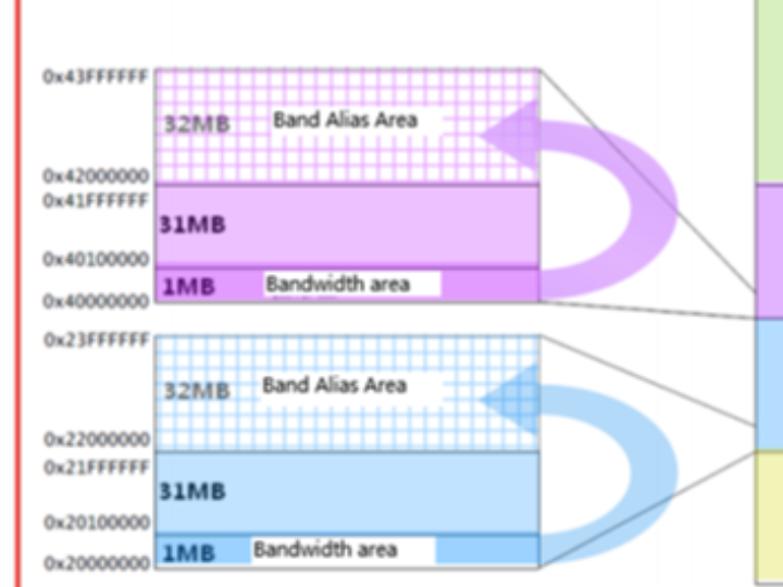
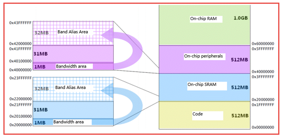
These two 1MB basic bit band areas not only have the regular storage operation functions, but also map to dedicated bit band alias areas. The bit band alias areas expand each bit of the basic bit band area to a 32-bit word (4 bytes) through a special mechanism. By accessing these expanded 32-bit words, precise operations can be achieved on the specified bits in the original basic bit band area. The relationship between memory mapping and bit band areas of W55MH32 can be referred to in the following figure:
1.2 Bit band area segmentation analysis
1.2.1 Peripheral bit area
The peripheral bit band address range is from 0X40000000 to 0X40100000 (1MB), covering all the registers of the on-chip peripherals of W55MH32 (register address range: 0X40000000 to 0X40029FFF). The corresponding bit band alias area address range is from 0X42000000 to 0X43FFFFFF (32MB), which precisely falls within the reserved address space of W55MH32 (0X40030000 to 0X4FFFFFFF), avoiding conflicts with the addresses of other peripheral registers.
Unlike the 51 single-chip microcontroller which only partially supports bit operations for registers (such as SBUF requires byte operations), all the on-chip peripheral registers of W55MH32 support bit band operations. This feature significantly enhances the flexibility of the underlying control. However, it should be noted that in practical projects, bit operations are usually not performed on all registers, and only in specific scenarios such as requiring high-frequency operation of IO ports, will IO-related registers be specifically enabled for bit operations.
1.2.2 SRAM bit band area
The address range of the SRAM bit band area is from 0X20000000 to 0X200FFFFF (1MB), and the corresponding bit band alias area address range is from 0X22000000 to 0X23FFFFFF (32MB). Due to the relatively low demand for bit operations in SRAM, the actual application scenarios of this area are relatively limited.
1.3 Bit-band address translation mechanism
When each bit of the bit band is expanded to a 32-bit word, only the least significant bit (LSB) is valid. Although it may seem that the space utilization is not high, this design matches the 32-bit system bus architecture of W55MH32 and ensures the maximum efficiency of 4-byte access.
1.3.1 Address Conversion Formula
By accessing the bit band alias area address through a pointer, operations on the bits of the basic bit band area can be performed. The specific conversion formula is as follows:
● Address of alias area for peripheral bit band: Let the byte address of a certain bit in the basic bit band area be A, and the bit position number be n (0 ≤ n ≤ 31, the actual range is determined by the register bit width). Then its address in the alias area is:
AliasAddr= =0x42000000+ (A-0x40000000)*8*4 +n*4Formula Explanation:
- 0x42000000: Starting address of the alias area for peripheral bits
- (A - 0x40000000): Number of bytes before the target bits
- ×8×4: Single byte 8 bits, each bit expanded to 4 bytes
- n×4: Offset of the target bits within a byte (each bit occupies 4 bytes)
- Address of the alias area for SRAM bit band: Let the byte address of a certain bit in the base bit band area be A, and the bit position number be n, then its address in the alias area is:
AliasAddr= =0x22000000+ (A-0x20000000)*8*4 +n*4Formula Explanation: The formula logic is consistent with the peripheral bit band area. Only the starting address (0x22000000) and the starting address of the base bit band area (0x20000000) are different.
1.3.2 Uniform macro definition
To simplify the operation, the two types of addresses can be combined into a unified macro definition:
#define BITBAND(addr, bitnum) ((addr & 0xF0000000)+0x02000000+((addr & 0x00FFFFFF)<<5)+(bitnum<<2))●addr & 0xF0000000: Extract the high-order bits (0x40000000 or 0x20000000) to distinguish between peripheral / SRAM regions
●+0x02000000: Convert the high-order bits to the starting address of the alias area (0x42000000 or 0x22000000)
●(addr & 0x00FFFFFF) << 5: Equivalent to (A - base area starting address) × 8 × 4 (shifting the high-order bits to the left by 5 positions = ×32 = ×8 × 4)
●bitnum << 2: Equivalent to n × 4 (shifting 2 positions to the left = ×4)
Together with the following macros, bit banding operations can be achieved:
2 Practical Operations of GPIO Bit Bands
2.1 GPIO Register Mapping
The peripheral bit area covers all on-chip peripheral registers. In theory, aliases for each register bit can be defined using macros. However, in actual development, bit operations are typically enabled only for high-frequency operation GPIO registers (such as output data register ODR and input data register IDR), as specified in the manual.
According to the manual, the offsets of GPIO's ODR and IDR registers relative to the GPIO base address are 12 and 8 (where GPIOx_BASE is defined by the library function). The specific register address mapping is as follows:
Code Listing: Bit Banding Operations - Mapping of GPIO ODR and IDR Registers
#define GPIOA_ODR_Addr (GPIOA_BASE+12) //0x4001080CNote: The number of GPIO ports may vary among different single-chip microcontroller models (for example, the 64-pin model can only support up to Port C at most). When using it in practice, adjustments should be made according to the specific model.
2.2 GPIO Bit Operation Macro Definitions
By using the bit-band alias address, it is possible to directly manipulate a single IO port of the specified GPIO port. The following are the macro definitions for GPIO input/output bit operations:
Code Listing: Bit Banding Operations - 2 GPIO Input/Output Bit Operations
#define PAout(n) BIT_ADDR(GPIOA_ODR_Addr,n) 2.3 Main function example
The following is an example of the main function for controlling GPIO through bit operations:
Code Listing: Bit Banding Operations - 3 Main Function
int main(void)WIZnet is a fabless semiconductor company founded in 1998. Its products include the Internet processor iMCU™, which utilizes TOE (TCP/IP Offload Engine) technology and is based on a unique patented fully hardwired TCP/IP. The iMCU™ is designed for embedded Internet devices in various applications.
WIZnet has more than 70 distributors globally and has offices in Hong Kong, South Korea, and the United States, providing technical support and product marketing services.
The regions managed by the Hong Kong office include Australia, India, Turkey, and Asia (excluding South Korea and Japan).