
Chapter 4: What Are Registers in W55MH32
Chapter 4: What Are Registers in W55MH32
Chapter 4: What Are Registers
References for this chapter: "W55MH32 Data Manual_V1.0.0", "W55MH32 Reference Manual_V1.0.0"
When studying this chapter, it will be more effective to read together with the "Memory and Bus Architecture" and "General I/O (GPIO)" sections of the "W55MH32 Reference Manual_V1.0.0", especially for the parts related to register explanations.
1. What is a register
We often talk about registers. So what are registers? This is the content we need to explain in this chapter. During the learning process, please think about this question carefully with your doubts, and at the end, see if you can give a definition of registers in one sentence.
2 W55MH32
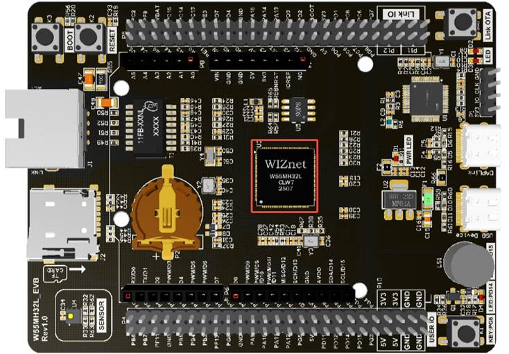
The chip used in our development board is the 100-pin W55MH32L. Please refer to the following picture for details. This is the high-performance Ethernet single-chip microcontroller that we will be learning about next. It will lead us into the realm of embedded systems.
The chip is surrounded by pins. In the development board, the pins of the chip are exposed and connected to various sensors. Then, programming is conducted on the W55MH32L (which is actually controlling these pins to output high or low voltage through the program) to control the operation of various sensors. Through experiments, we can learn about the various resources of the W55MH32 chip. The development board is an evaluation board, with abundant onboard resources and a high degree of pin reutilization. The aim is to verify all the functions of the chip on a single board.
3 What is inside the chip
The chips we see are already packaged finished products, mainly consisting of the core and on-chip peripherals. If compared to a computer, the core and peripherals are like the CPU and motherboard, memory, graphics card, and hard drive in a computer.
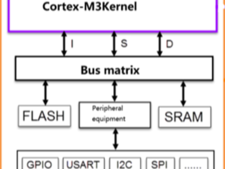
The W55MH32 uses the Cortex-M3 core. The core is the CPU and is responsible for designing components outside the core and producing the entire chip. These components outside the core are called off-core peripherals or on-chip peripherals. Such as GPIO, USART (serial port), I2C, SPI, etc., are all called on-chip peripherals.
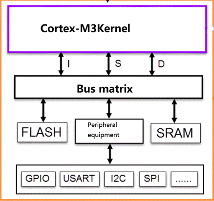
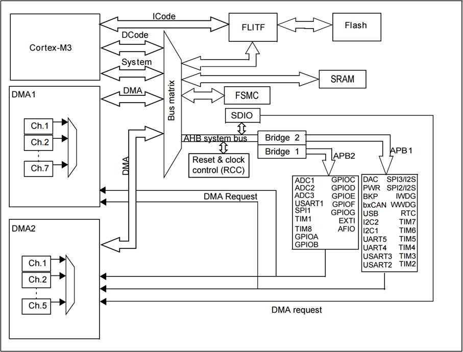
The chip (which refers to the core or CPU) is connected to the peripherals through various buses. There are 4 driver units and 4 passive units. Please refer to Figure W55MH32 for the system diagram. For ease of understanding, we can consider the driver units as the CPU part and the passive units as the peripherals. Now, let's briefly introduce the various components of the driver units and the passive units.
3.1 ICode Bus
In ICode, the "I" stands for "Instruction", which means "command". The programs we write are all composed of individual instructions after compilation, and they are stored in FLASH. For the kernel to read these instructions and execute the program, it must use the ICode bus. It is almost always in use and is specifically designed for fetching instructions.
3.2 Drive unit
3.2.1 DCode Bus
In DCode, the "D" stands for "Data", meaning that this bus is used for data retrieval. When we write programs, there are two types of data: constants and variables. Constants are fixed and unchangeable, and they are defined using the "const" keyword in C language and stored in the internal FLASH. Variables, on the other hand, are variable and can be changed. Whether they are global or local variables, they are stored in the internal SRAM. Since data can be accessed by the Dcode bus and the DMA bus, to avoid access conflicts, a bus matrix is used to arbitrate and determine which bus is used for data retrieval.
3.2.2 System bus
The system bus is mainly used to access the registers of external devices. The so-called register programming, which involves reading and writing registers, is accomplished through this system bus.
3.2.3 DMA bus
The DMA bus is mainly used for data transmission. This data can be in the data registers of a certain peripheral device, in SRAM, or in the internal FLASH. Since the data can be accessed by the Dcode bus and the DMA bus, in order to avoid access conflicts, a bus matrix needs to be used to arbitrate and determine which bus is used for data retrieval.
3.3 Passive unit
3.3.1 Internal flash memory
The internal flash memory, known as FLASH, is where our compiled programs are stored. The kernel retrieves the instructions from this area via the ICode bus.
3.3.2 Internal SRAM
The internal SRAM, which is what we commonly refer to as RAM, the overhead of program variables, stack, etc., is all based on the internal SRAM. The kernel accesses it through the DCode bus.
3.3.3 FSMC
The full English name of FSMC is Flexible Static Memory Controller, which is called a distinctive peripheral in the W55MH32. Through FSMC, we can expand the memory, such as external SRAM, NANDFLASH and NORFLASH. However, there is one point we need to pay attention to: FSMC can only expand static memory, that is, the "S" in the name stands for static, and it cannot be dynamic memory, such as SDRAM cannot be expanded.
3.3.4 The bridge from AHB to APB
Two APB2 and APB1 buses extending from the AHB bus are equipped with various special peripherals of W55MH32. The GPIO, serial port, I2C, SPI and other peripherals we often talk about are all mounted on these two buses. This is the key point for us to learn about W55MH32, which is to learn how to program these peripherals to drive various external devices.
4 Memory mapping
In the W55MH32 system block diagram, the program memory, data memory, registers and input/output ports are organized within the same 4GB linear address space. Data bytes are stored in the memory in little-endian format. The lowest address byte in a word is considered to be the lowest effective byte of the word, while the highest address byte is the highest effective byte. The accessible memory space is divided into 8 main blocks, each of which is 512MB. During programming, we can find them by their addresses and then operate on them (by using C language to read and write data to them).
4.1 Memory mapping
The memory itself does not have address information. Its address is assigned by the chip manufacturer or the user. The process of assigning addresses to the memory is called memory mapping. Please refer to the figure "Memory Mapping" for details. If another address is assigned to the memory, it is called memory re-mapping.
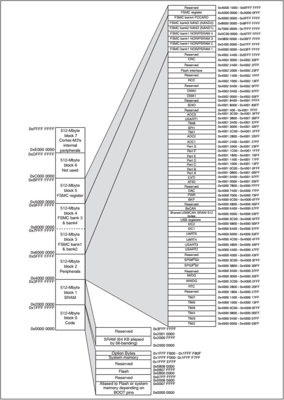
4.1.1 Function division of memory area
In this 4GB address space, ARM has roughly divided it into 8 blocks, each of 512MB. Each block is also assigned a specific purpose, as detailed in the table "Memory Function Classification". Each block is 512MB in size. Clearly, this is a very large size. When chip manufacturers design unique peripherals within each block, they may not necessarily use up the entire space; they only utilize a portion of it.
Serial Number | Purpose | Address range |
Block 0 | Code | 0x0000 0000 ~ 0x1FFF FFFF(512MB) |
Block 1 | SRAM | 0x2000 0000 ~ 0x3FFF FFFF(512MB) |
Block 2 | On-chip peripherals | 0x4000 0000 ~ 0x5FFF FFFF(512MB) |
Block 3 | FSMC's bank1 to bank2 | 0x6000 0000 ~ 0x7FFF FFFF(512MB) |
Block 4 | FSMC's bank3 to bank4 | 0x8000 0000 ~ 0x9FFF FFFF(512MB) |
Block 5 | FSMC register | 0xA000 0000 ~ 0xCFFF FFFF(512MB) |
Block 6 | Not used | 0xD000 0000 ~ 0xDFFF FFFF(512MB) |
Block 7 | Internal peripherals of Cortex-M3 | 0xE000 0000 ~ 0xFFFF FFFF(512MB) |
Among these 8 blocks, 3 of them are very important and are the ones we are most concerned about. Block 0 is designed to be the internal FLASH, Block 1 is designed to be the internal RAM, and Block 2 is designed to be the on-chip peripherals. Now, let's briefly introduce the functional division of the specific areas within these three blocks.
4.1.1.1 Function division of the internal area of Memory Block 0
Block0 is mainly used for designing the on-chip FLASH. Integrating a larger FLASH or SRAM within the chip would mean an increase in the chip cost. Usually, the on-chip integrated FLASH is not very large. The W55MH32 can achieve 512KB while pursuing cost-effectiveness, which is truly a considerate move. The specific function division of the internal areas of the Block is shown in the table: Function Division of Internal Areas of Memory Block 0.
Block | Usage Instructions | Address range |
Block0 | Reserve | 0x1FFE C008 ~ 0x1FFF FFFF |
Option bytes: Used for configuring read/write protection, BOR level, software/hardware watchdog, and reset when the device is in standby or stop mode. After the chip is locked, the corresponding register bits can be modified by starting from RAM. | 0x1FFF F800 - 0x1FFF F80F | |
System memory: Stores the ISP self-initiating program (Bootloader) that was pre-written by ST at the factory. Users cannot modify this program. This program is required for serial port download. | 0x1FFF F000 - 0x1FFF F7FF | |
Reserve | 0x0808 0000 ~ 0x1FFF EFFF | |
FLASH:Program storage location | 0x0800 0000 ~ 0x0807 FFFF (512KB) | |
Reserve | 0x0008 0000 ~ 0x07FF FFFF | |
Depending on the BOOT pin, it can be used as the alias for FLASH, system memory, or SRAM. | 0x0000 0000 ~ 0x0007 FFFF |
4.1.1.2 Function division of the internal area of Memory Block 1
Block1 is used for designing the on-chip SRAM. The specific functional division of the internal area of Block is shown in the table. Functional division of the internal area of Memory Block1.
Block | Usage Instructions | Address range |
Block1 | Reserve | 0x2001 0000 ~ 0x3FFF FFFF |
SRAM 64KB | 0x2000 0000 ~ 0x2000 FFFF |
4.1.1.3 Function division of the internal area of Memory Block 2
Block2 is used for designing the on-chip peripherals. Depending on the bus speed of the peripherals, Block is divided into two parts: APB and AHB. Among them, APB is further divided into APB1 and APB2. Please refer to the table "Functional Division of Internal Areas of Block2 for Memory" for details.
Block | Usage Instructions
| Address range
|
Block2 | APB1 Bus peripheral | 0x4000 0000 ~ 0x4000 77FF |
APB2 Bus peripheral | 0x4001 0000 ~ 0x4001 3FFF | |
AHB Bus peripheral | 0x4001 8000 ~ 0x5003 FFFF |
5 Register mapping
We know that the memory itself has no addresses. The process of assigning addresses to the memory is called memory mapping. Then, what is register mapping? What exactly is a register?
In the Block2 area of the memory, what is designed are on-chip peripherals. They are organized in units of four bytes, totaling 32 bits. Each unit corresponds to a different function. When we control these units, we can drive the peripherals to work. We can find the starting address of each unit, and then access these units using the pointer operation method in C language. If we access each time through this address method, it is not easy to remember and prone to errors. At this time, we can give this memory unit an alias based on its function, and this alias is what we often call a register. This process of giving an alias to the memory unit with a specific function that has been assigned an address is called register mapping.
For example, we find that the address of the output data register ODR of the GPIOB port is 0x40010C0C (as for how to find this address, you can skip it for now. We will have a detailed explanation later). The ODR register is 32 bits, with the lower 16 bits being valid, corresponding to 16 external IOs. Writing 0/1 to the corresponding IOs outputs low/high levels. Now, through the pointer operation method in C language, we make all 16 IOs of GPIOB output high levels. See the code list: Register - 1.
Code listing: Register -1 accesses memory units through absolute addresses
*(unsigned int*)(0x4001 0C0C) = 0xFFFF;0x4001 0C0C is regarded as the address of the ODR of GPIOB port in our view. However, from the compiler's perspective, it is just an ordinary variable, an immediate number. To make the compiler also consider it as a pointer, we need to perform a forced type conversion and convert it into a pointer, that is, (unsigned int *)0x4001 0C0C. Then, we need to perform the * operation on this pointer.
Just now, we mentioned that accessing memory units through absolute addresses is not easy to remember and prone to errors. We can operate through registers instead. Please refer to the code list: Register - 2.
Code Listing: Register - 2 Accessing Memory Units via Register Alias Method
// All the GPIOB ports are set to output a high level.To facilitate the operation, we simply defined the pointer operation "*" within the register alias as well. Please refer to the code listing: Register-3 for details.
Code listing: Register-3 accesses memory units through register aliases
// All the GPIOB ports are set to output a high level.5.1 The peripheral address mapping of W55MH32
The on-chip peripheral devices are divided into three buses. Depending on the speed of the peripherals, different buses are equipped with different peripherals. APB1 is used for low-speed peripherals, while APB2 and AHB are used for high-speed peripherals. The lowest address of each corresponding bus is referred to as the base address of that bus. The base address of the bus is also the address of the first peripheral device mounted on that bus. Among them, the address of the APB1 bus is the lowest. The on-chip peripherals start from here and are also called the peripheral base address.
5.1.1 Bus base address
Bus name | Bus base address | Offset relative to the peripheral base address |
APB1 | 0x4000 0000 | 0x0 |
APB2 | 0x4001 0000 | 0x0001 0000 |
AHB | 0x4001 8000 | 0x0001 8000 |
The "relative peripheral base address offset" of the table bus base address is the difference between this bus address and the "on-chip peripheral" base address 0x4000 0000. We will discuss the offset of the address later.
5.1.2 Peripheral device base address
Within the address range of XX peripheral device, the registers of that peripheral device are distributed. Taking the GPIO peripheral as an example, GPIO is the abbreviation for General Purpose Input/Output Port. In simple terms, it refers to the pins that W55MH32 can control. Its basic function is to control the output of high or low voltage on the pins. The simplest application is to connect the GPIO pin to the cathode of the LED light, connect the anode of the LED light to the power supply, and then control the voltage level of this pin through W55MH32, thereby achieving the control of the LED light's on/off.
GPIO has many registers, each with a specific function. Each register is 32 bits in size, occupying four bytes, and is arranged sequentially at the base address of this peripheral. The position of each register is described by the offset address relative to the base address of the peripheral. Here, we take the GPIOB port as an example to illustrate which registers are available in GPIO. Please refer to the table for the register address list of the GPIOB port: GPIOB Port Register Address List:
Bus name | Bus base address | Offset relative to the base address of GPIOB |
GPIOB_CRL | 0x4001 0C00 | 0x00 |
GPIOB_CRH | 0x4001 0C04 | 0x04 |
GPIOB_IDR | 0x4001 0C08 | 0x08 |
GPIOB_ODR | 0x4001 0C0C | 0x0C |
GPIOH_BSRR | 0x4001 0C10 | 0x10 |
GPIOH_BRR | 0x4001 0C14 | 0x14 |
GPIOH_LOCKR | 0x4001 0C18 | 0x18 |
The register descriptions for peripherals can be referred to in the specific chapters of the "W55MH32 Reference Manual". When programming, we need to repeatedly consult the register descriptions of the peripherals.
Here, we take the "GPIO Port Set/Reset Register" as an example to teach you how to understand the register descriptions. Please refer to the figure "GPIO Port Set/Reset Register Description".
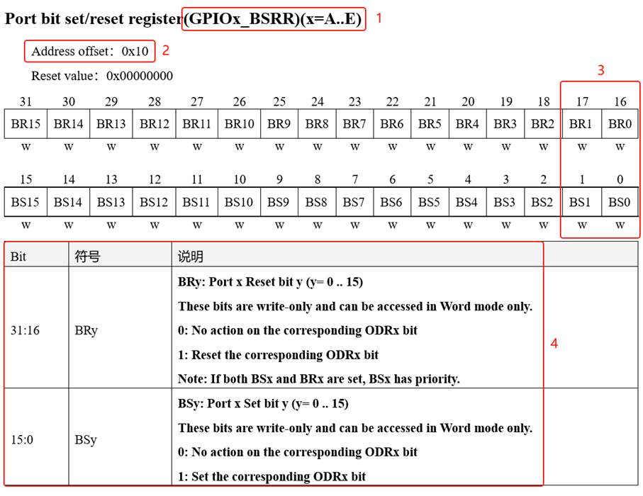
1. Name
The register description begins by listing the name of the register, "(GPIOx_BSRR)(x=A...E)". The meaning of this part is that the register is named "GPIOx_BSRR", where "x" can be A to E. That is to say, this register description is applicable to GPIOA, GPIOB to GPIOE, and these GPIO ports all have such a register.
2. Offset Address
The offset address refers to the offset of this register relative to the base address of this peripheral. The offset address of this register is 0x10. From the reference manual, we can find that the base address of the GPIOA peripheral is 0x4001 0800. Therefore, the address of the GPIOA_BSRR register of this GPIOA can be calculated as: 0x4001 0800 + 0x10. Similarly, since the base address of the GPIOB peripheral is 0x4001 0C00, the address of the GPIOB_BSRR register can be calculated as: 0x4001 0C00 + 0x10. For other GPIO ports, this method can be applied accordingly.
3 Register Bit Table
Next comes the bit table of this register, which lists the names and permissions of its bits 0 to 31. The numbers above the table are the bit numbers, the middle part is the bit name, and the bottom part is the read/write permission. Among them, 'w' indicates write-only, 'r' indicates read-only, and 'rw' indicates read-write. The bit permissions of this register are all 'w', so it can only be written. If you read this register, you cannot guarantee that you will read its true content. Some register bits are read-only, and they are generally used to represent a certain working state of the W55MH32 peripheral. This state is automatically changed by the W55MH32 hardware, and the program reads those register bits to determine the working state of the peripheral.
4 Function Descriptions
The bit function is the most important part of the register description. It elaborates on the function of each bit of the register. For example, in this register, there are two register bits, namely BRy and BSy. The value of y can be 0-15. Here, 0-15 represents the pin number of the port. For instance, BR0 and BS0 are used to control the 0th pin of GPIOx. If x represents GPIOA, then it controls the 0th pin of GPIOA, while BR1 and BS1 control the 1st pin of GPIOA.
The description for the BRy pin is "0: no operation will be performed on the corresponding ODRx bit; 1: the corresponding ODRx bit will be reset". Here, "reset" means setting the bit to 0, while "set" means setting the bit to 1. The "ODRx" in the description refers to the register bit of another register, and we only need to know that when the ODRx bit is 1, the corresponding pin x outputs a high level, and when it is 0, the corresponding pin outputs a low level (interested readers can consult the description of the register GPIOx_ODR to learn more). Therefore, if "1" is written to BR0, then the 0th pin of GPIOx will output a "low level", but if "0" is written to BR0, it will not affect the ODR0 bit, so the pin level will not change. To make the pin output a "high level", "1" needs to be written to the "BS0" bit, and the register bits BSy and BRy are opposite operations.
5.2 C language's encapsulation of registers
All the above content related to memory mapping is ultimately aimed at helping everyone better understand how to control the reading and writing of peripheral registers using C language. This is the key point of this chapter.
5.2.1 Encapsulate the base addresses of the bus and peripherals
In programming, for the purpose of facilitating understanding and memory, we have defined the bus base address and the peripheral base address as corresponding macros. The bus or the peripheral is named as the macro name. Please refer to the code listing: Register-4 for details.
Code Listing: Register-4 Bus and Peripheral Base Address Macro Definitions
#define PERIPH_BASE ((unsigned int)0x40000000)Code Listing: Register - 4 Firstly, the "on-chip peripheral" base address PERIPH_BASE is defined. Then, the address offsets of each bus are added to PERIPH_BASE to obtain the addresses of APB1 and APB2 buses, namely APB1PERIPH_BASE and APB2PERIPH_BASE. The address offsets of peripherals are added above them to obtain the peripheral addresses of GPIOA-G. Finally, the address offsets of each register are added to the peripheral addresses to obtain the addresses of specific registers. Once the specific addresses are available, they can be read and written using pointers. Please refer to Code Listing: Register - 5 for details.
Code Listing: Register - 5 Using Pointers to Control the BSRR Register
*(unsigned int *)GPIOB_BSRR = (0x01<<(16+0));This code uses (unsigned int *) to forcibly convert the value of the GPIOB_BSRR macro into an address, and then uses the "*" symbol for pointer operation to assign the value to this address, thereby achieving the function of writing to the register. Similarly, for reading the register, the pointer operation is used to retrieve the data in the register and store it in a variable, thereby obtaining the status of the W55MH32 peripheral.
5.2.2 Encapsulated register list
Using the above method to define addresses is still a bit cumbersome. For example, GPIOA to GPIOE each have a group of registers with the same functions, such as GPIOA_ODR/GPIOB_ODR/GPIOC_ODR, etc. They only have different addresses, but we still need to define the address for each register. To facilitate accessing the registers, we introduce the structure syntax in C language to encapsulate the registers. Please refer to Code List: Registers - 6 for details.
Code Listing: Register - 6 Encapsulation of GPIO Register Group Using Structs
typedef unsigned int uint32_tThis code uses the `typedef` keyword to declare a structure type named `GPIO_TypeDef`. The structure contains 7 member variables, and the variable names exactly correspond to the names of the registers. According to the syntax rules of C language, the storage space for variables within a structure is contiguous. 32-bit variables occupy 4 bytes, and 16-bit variables occupy 2 bytes. Please refer to the address offset of the structure members in the figure for details. GPIO_TypeDef structure member addresses.
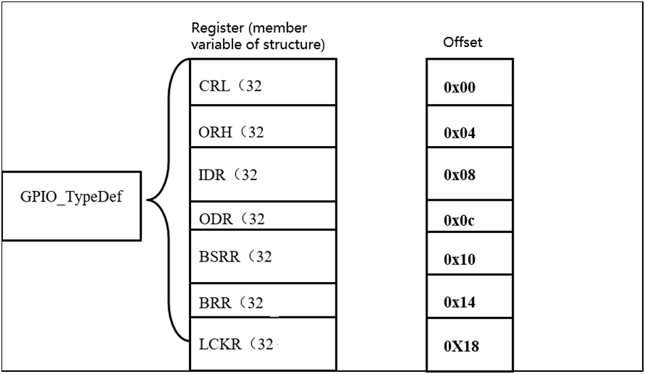
That is to say, if the starting address of this GPIO_TypeDef structure is 0x4001 0C00 (which is also the address of the first member variable CRL), then the address of the second member variable CRH in the structure is 0x4001 0C00 + 0x04. This 0x04 represents the offset of the 4-byte address occupied by CRL. The offsets of other member variables relative to the starting address of the structure are already explained in the comments on the right side of the above code.
Such address offset corresponds one-to-one with the register address offset defined by the W55MH32 GPIO peripheral. As long as the starting address of the structure is set properly, the addresses of the members within the structure can be determined, and then the registers can be accessed in the form of a structure. Please refer to the code listing: Register-7 for details.
Code Listing: Register - 7 Accessing Registers via Structure Pointers
GPIO_TypeDef * GPIOx; This code first defines a structure pointer GPIOx of type GPIO_TypeDef, and makes the pointer point to the address GPIOB_BASE (0x4001 0C00). With this address determined, it then follows the C language syntax for accessing the structure to read and write the registers using methods such as GPIOx->ODR and GPIOx->IDR.
Finally, we take it a step further and directly use a macro definition for the pointer of the GPIO_TypeDef type. The pointer points to the starting address of each GPIO port. When using it, we can directly access the registers using this macro. The specific code listing: Register - 8.
Code listing: Register-8 defines the initial address and pin of the GPIO port.
#define GPIOA ((GPIO_TypeDef *) GPIOA_BASE)Here, we take the GPIO peripheral as an example to explain to you how C language encapsulates registers. By analogy, other peripherals can also be encapsulated in the same way. The good news is that this part of the work has been completed by the firmware library for us. Here, we only analyzed the process of this encapsulation to let you know what it is, and also to explain why it is so.
5.3 The method for modifying the bits of a register through operations
When assigning values to registers using C language, we often need to modify only certain bits of a specific register while keeping the other bits of the register unchanged. In such cases, we need to utilize the bit manipulation methods provided by C language.
5.3.1 Set a certain bit of the variable to zero
Here, we use the variable 'a' to represent the register, and assume that there is already a value in the register. At this point, we need to clear a certain bit of the variable 'a' while keeping the other bits unchanged. The method can be found in the code listing: Register - 9.
Code snippet: Clearing a bit in register -9
unsigned char a = 0x9f;Since sometimes several consecutive bits in the register are used to control a certain function, let's assume that we need to clear certain consecutive bits of the register while keeping the other bits unchanged. The method is shown in the code listing: Register-10.
Code snippet: Clearing certain consecutive bits in register -10
// If the binary bits in a are divided into groups of 25.3.3 Assign values to certain bits of the variable
After the above clearing operation on the register bits, it becomes convenient to write the desired values to certain bits while keeping the other bits unchanged. The method is shown in the code listing: Register-11. At this time, the written value is generally the parameter for setting the bits of the register.
Code listing: Assign values to certain bits of register -11
//a = 1000 0011 b

a |= (1<<2*2);
5.3.4 Inverting a certain bit of the variable
In some cases, we need to perform an inversion operation on a certain bit of the register, that is, changing 1 to 0 and 0 to 1. This can be directly achieved through the following operation, while the other bits remain unchanged. See the code listing: Register - 12.
Code snippet: Perform an inversion operation on a specific bit using register -12
//a = 1001 0011 b
WIZnet is a fabless semiconductor company founded in 1998. Its products include the Internet processor iMCU™, which utilizes TOE (TCP/IP Offload Engine) technology and is based on a unique patented fully hardwired TCP/IP. The iMCU™ is designed for embedded Internet devices in various applications.
WIZnet has more than 70 distributors globally and has offices in Hong Kong, South Korea, and the United States, providing technical support and product marketing services.
The regions managed by the Hong Kong office include Australia, India, Turkey, and Asia (excluding South Korea and Japan).