
Chapter 33: W55MH32’s OTP - One-Time Programming Area Read/Write
Chapter 33: W55MH32’s OTP - One-Time Programming Area Read/Write
Chapter 32: W55MH32’s OTP - One-Time Programming Area Read/Write
The OTP (One-Time Programmable, one-time programmable memory) of W55MH32 is a special non-volatile storage area within the chip, mainly used to store critical data that needs to be written once and cannot be erased. The following provides detailed explanations from aspects such as functional characteristics, typical applications, programming design, and precautions:
OTP Functionality Characteristics
Non-volatile
The data stored in the OTP can be retained even after the chip loses power, without the need for an additional power supply, similar to Flash and EEPROM.
Physical Protection Mechanism
The writing of OTP is usually achieved through fusing (Fuse) or special processes (such as anti-fuses). The writing operation permanently alters the physical state of the storage unit (such as fusing the metal connection), thereby ensuring that the data cannot be tampered with.
The W55MH32 is an OTP with an anti-fuse process, which has the characteristic of "only allowing the writing of 1 (transforming the unprogrammed 0 into 1), and not allowing the writing of 0 (the programmed 1 cannot be restored to 0)".
The principle of anti-fuse OTP is as follows:
- Initial state (unprogrammed): The storage unit is in a logical 0 state (such as when the anti-fuse has not been broken, it is equivalent to high resistance or a capacitor, representing 0).
- Programming process: A high voltage is applied to break the anti-fuse, and the unit becomes a logical 1 state (equivalent to low resistance, representing 1). Once programmed (writing 1), it cannot be reversed back to 0 (the physical structure is irreversible).
Compared with the fuse-type OTP:
- Fuse type: Initially set to 1 (the fuse has not blown), when programmed, the fuse blows and the unit becomes 0 (can only be written as 0, not 1).
- Anti-fuse type: Initially set to 0, after programming it becomes 1 (can only be written as 1, not 0), which conforms to the description of "writing 1 is irreversible".
One-time Write Limitation
The OTP area of W55MH32 only allows each storage unit (typically a bit or a byte) to be written to once (some models support block/page writing, but overall it is still one-time writing). Once written, it cannot be erased or overwritten, so the data accuracy must be ensured before writing.
Access Control
The OTP area of W55MH32 supports write protection (locked by registers). The write permission can only be enabled through a specific instruction (writing the unlock key) to prevent accidental operations.
Application Scenarios
The "one-time write + non-volatile" feature of OTP makes it suitable for the following scenarios:
Unique Identifier (UID) Storage
When the chips are manufactured, the manufacturer may write a globally unique device ID (such as a 96-bit or longer code) into them, which is used for product traceability, anti-counterfeiting or encryption authentication (for example, as the seed for an AES key).
Calibration Parameter Storage
The calibration data (such as offsets and gain coefficients) of sensors or analog modules (such as ADC and DAC) need to be written into OTP through testing equipment before leaving the factory to prevent data loss due to the limitation of Flash erasing times.
Security Key Storage
It is used to store encryption keys (such as AES-128/256 keys, HMAC keys) or security configurations (such as lock positions that prevent JTAG debugging). Due to the non-erasable nature of OTP, even if the chip is subject to physical attacks, the keys are difficult to be tampered with or stolen.
Customer Customized Data
The equipment manufacturer can input customer-specific information (such as hardware version and regional configuration) during the production stage, thereby avoiding the costs associated with subsequent software modifications.
Notes
Number of Write Operations Limit
Each storage unit of the OTP can only be written to once (supporting bit-wise writing, but multiple writes to the same bit will be regarded as a one-way operation from "0" to "1"). If an attempt is made to write to the same address repeatedly, it may lead to data errors or hardware lockup.
Voltage and Timing Requirements
The writing of OTP requires a stable power supply (usually it needs to meet the minimum voltage specified in the chip manual, such as 2.7V to 3.6V), and the writing timing sequence must strictly follow the data manual (such as the writing pulse width, address setup time).
Safety Risks
Some OTP areas may be associated with the security mechanisms of the chip (such as read protection, debug interface locking). Incorrect writing may result in the inability to debug the chip or functional failure. Therefore, operations should be carried out with caution.
Program Design
The following is the program design process of the OTP routine:
Power-on of OTP
Before using the OTP module, we need to provide it with a stable power supply. By configuring the system clock, unlocking the protection mechanism, and setting the startup time of the low-dropout regulator (LDO), we ensure that the power supply meets the requirements during the operation (such as writing the fuse). This is mainly achieved through the OTP_PowerOn() function, as follows:
void OTP_PowerOn(uint32_t Time)The OTP_PowerOn() function is the power initialization function for the OTP module, mainly used to configure the power supply timing of the OTP to ensure its stable operation: Firstly, by setting RCC->RCC_SYSCFG_CONFIG = 0x01, the SYSCFG module clock is enabled, providing the basis for subsequent configuration; then, the unlock key 0xAB12DFCD is written to SYSCFG->SYSCFG_LOCK to unlock the protection and allow modification of the OTP power parameters; finally, based on the input Time, the startup time of the OTP LDO (Low Dropout Regulator) is configured - if Time is greater than the preset minimum startup time OTP_POWERON_TIME, then use Time, otherwise force the use of the minimum value, in order to balance the power supply stability and efficiency, and avoid the failure of OTP operation (such as writing fuse) due to power supply fluctuations or insufficient startup time.
Set the time benchmark
The OTP_SetTime() function provides precise control over the duration for which the write (bistable or anti-bistable) operation of OTP is powered by a controlled voltage:
void OTP_SetTime(uint16_t Time)The OTP_SetTime() function achieves this by performing a bitwise OR operation on the input Time parameter to the OTP_10ns register, adding configuration parameters for OTP operation time (such as write pulse width) in units of 10 nanoseconds. This ensures that the voltage/current application time meets the requirements for OTP physical state changes, thereby guaranteeing the reliability of data writing. This design takes into account both the flexibility and security of time configuration, allowing developers to dynamically adjust the key timing according to actual needs.
Writing Data
The OTP_WriteByte() function is used to write a byte of data to the specified address in the OTP. The details are as follows:
void OTP_WriteByte(uint8_t Addr,uint8_t Data)The OTP_WriteByte() function achieves the function of writing a single byte of data to the specified address in the OTP through a closed-loop process of "address verification → data loading → triggering write → waiting for completion". Its core lies in operating the registers of the OTP module and collaborating with the hardware to complete the modification of the physical state of the storage unit, ensuring the one-time and reliable writing of the data.
OTP Power Failure
The OTP_PowerOff() function is used to shut down the power supply of the OTP module or put it into a low-power mode. It is usually called after the OTP operation is completed to reduce system power consumption or prevent accidental writing. The core logic of this function is to unlock the protection register and disable the relevant clock, thereby cutting off the power supply to the OTP module or configuring it to enter a sleep state. The function content is as follows:
void OTP_PowerOff(void)The function first writes the unlock key to SYSCFG_LOCK to remove the protection, then disables the SYSCFG clock through RCC_SYSCFG_CONFIG, and finally cuts off the power supply to OTP or puts it into sleep mode.
Main Function main()
The main function main() is as follows:
int main(void)The program first initializes the system clock (enabling the PWR and BKP peripheral clocks), delay functions and serial port (with a baud rate of 115200), and obtains the frequencies of all system clocks (such as SYSCLK, PCLK2, etc.) through RCC_GetClocksFreq, and prints to verify the clock configuration. Then, it starts the OTP power supply (OTP_PowerOn, with a startup time of 100ms based on the PCLK2 frequency), sets the OTP write timing (OTP_SetTime, with a time parameter of 1μs based on the PCLK2 frequency), and writes the data 0x5A to the 0th address of OTP. Subsequently, it reads and prints the 8 data registers of OTP (DATA0 to DATA7) to verify the successful write operation. Finally, it turns off the OTP power supply (OTP_PowerOff) to reduce power consumption and enters an infinite loop to maintain operation.
Overall, through initialization, clock verification, OTP configuration, write-read verification and power management, the OTP function is tested.
Download Verification
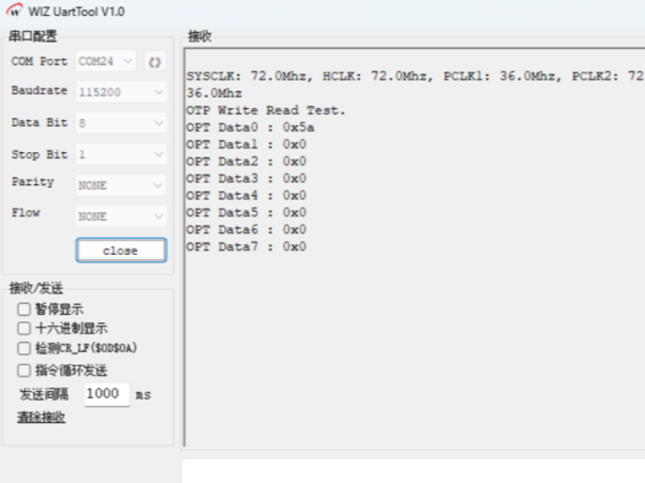
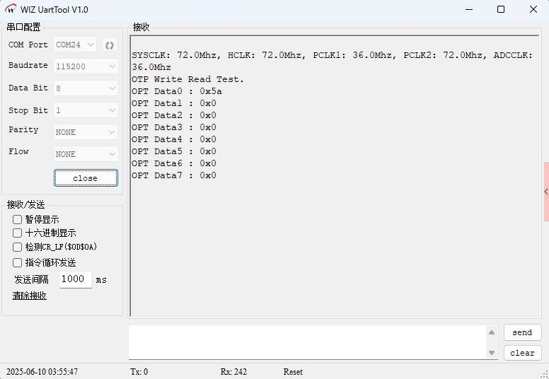
After the program is downloaded and run, the serial port output shows that the system clock (such as SYSCLK 72 MHz) is configured normally. The OTP test shows that the address 0 (DATA0) was written successfully with 0x5A, and the remaining addresses are default 0x0. This verifies the OTP writing and reading functions:
Summary
The OTP of W55MH32 is a non-volatile memory specifically designed for "one-time critical data storage", and its core value lies in the immutability of the data. In practical applications, it is necessary to combine the data manual of the chip model and strictly follow the writing process to ensure the accuracy and reliability of the data.
WIZnet is an off-chip semiconductor company founded in 1998. Its products include the Internet processor iMCU™, which adopts TOE (TCP/IP offloading engine) technology and is based on a unique patented fully hardwired TCP/IP. iMCU™ is designed for embedded Internet devices in various applications.
WIZnet has over 70 distributors worldwide, with offices in Hong Kong, South Korea, and the United States, providing technical support and product marketing.
The region managed by the Hong Kong office includes: Australia, India, Turkey, and Asia (excluding South Korea and Japan).