
Chapter 32: W55MH32’s MPU - Memory Protection Unit
Chapter 32: W55MH32’s MPU - Memory Protection Unit
Chapter 32: W55MH32’s MPU - Memory Protection Unit
The MPU (Memory Protection Unit) is a crucial module in the W55MH32 that is responsible for managing the access permissions and attributes of memory regions. It divides memory areas and sets access rules (such as read/write/execute permissions, cache policies), thereby enhancing the security and stability of the system. It is particularly suitable for multi-tasking systems (such as RTOS) or scenarios where critical resources need to be isolated.
Overview of MPU Function
Basic Concepts
MPU is a hardware module built into the W55MH32. It does not support virtual memory (different from MMU), but it can achieve the following functions by dividing the physical memory area:
- Restrict the access of tasks/programs to specific memory areas (such as prohibiting writing or execution).
- Define the attributes of memory areas (such as caching policies, sharing), optimize system performance.
- Detect illegal memory accesses (such as out-of-bounds, permission violations), trigger exceptions (such as MemManage Fault), prevent system crashes.
Key Terms
- Memory Region: The MPU divides the memory into multiple independent regions, and each region requires configuration of base address, size, permissions, etc.
- Access Permission: Defines the read (R), write (W), and execute (X) permissions of the region (such as read-only, read-write, non-executable).
- Memory Attribute: Includes cache policies (such as no cache, write-through, write-back), sharing (whether shared by multiple processors), etc., which affect the efficiency of data access.
Core Functions of MPU
Memory Area Division
The MPU divides the physical memory into multiple independent regions by configuring the base address and size of the regions.
- Size Limitation: The size of the area must be a power of 2 (such as 32B, 64B, 1KB, 64KB, etc.), and the base address must be aligned to the size of the area (for example, the base address of a 64KB area must be an integer multiple of 64KB).
- Area Overlap: If multiple areas overlap, the area with the higher number has a higher priority (covering the configuration of the smaller-numbered area).
Access Control
Each region can independently set the access permissions of privileged level (Privileged) and unprivileged level (Unprivileged) (for example, the kernel runs at the privileged level while tasks run at the unprivileged level in RTOS). Common permission combinations are as follows:
Permission Type | Description |
PRIV_RW | Privileged level: readable and writable; User level: no permission |
PRIV_RW_USER_RO | Privileged level: readable and writable; User level: read - only |
PRIV_RO | Privileged level: read - only; User level: no permission |
NO_ACCESS | Unaccessible at any level (used to mark illegal regions) |
Memory Attribute Configuration
By setting the memory type and cache policy, the efficiency of data access can be optimized:
- Memory type: such as normal memory (Normal), device memory (Device).
- Normal memory: supports caching (such as variables in SRAM).
- Device memory: usually consists of peripheral registers (such as GPIO, UART), and caching needs to be disabled (to avoid the read/write delay caused by caching).
- Normal memory: supports caching (such as variables in SRAM).
- Cache Strategy:
- Non-Cacheable: Direct access to physical memory (such as device registers).
- Write-Through: Writes data and simultaneously updates both the cache and the memory (suitable for scenarios requiring real-time performance).
- Write-Back: Writes data and only updates the cache, then writes it to the memory uniformly later (suitable for scenarios with frequent read and write operations, improving efficiency).
- Non-Cacheable: Direct access to physical memory (such as device registers).
Application Scenarios
The core value of MPU lies in memory security protection and resource isolation. Here are its typical application scenarios, along with explanations of their practical significance based on its core functions:
- RTOS Task Isolation (Core Requirement of Multi-tasking System): In an RTOS (Real-Time Operating System), multiple tasks share the same memory space. If not isolated, it may cause system crashes due to task abnormalities (such as stack overflow, wild pointers). MPU achieves task isolation through area division and permission control.
- Protection of Critical Data/Code (Anti-tampering and Error Prevention): In the system, certain data or code (such as firmware, calibration parameters, encryption keys) once modified may lead to functional failure or security vulnerabilities. MPU protects these resources by implementing read-only or prohibiting access permissions.
- Access Control for Peripheral Register (Preventing External Device Maloperation): Incorrect modification of peripheral register (such as GPIO, UART control registers) may cause external device abnormalities. MPU restricts only privileged-level code (such as the kernel) from modifying critical registers.
- Memory Boundary Exceedance Detection (Development and Debugging Aid): During the development stage, the program may access unallocated memory through array out-of-bounds, wild pointers, etc. MPU configures unused memory areas as NO_ACCESS (no access permission) and triggers an exception to quickly locate the problem.
- Security Boot and Firmware Protection (System-level Security Requirement): In systems that require secure boot (such as medical devices, industrial control), MPU protects the boot code and security configuration areas to ensure the system starts from trusted code.
Notes
Pin drive capability: The output frequency of MCO should not be too high (it should be lower than the maximum reliable frequency of GPIO, and it is usually recommended not to exceed 50 MHz). When operating at high frequencies, signal integrity (such as impedance matching) needs to be considered.
Clock source enable sequence: Before configuring MCO, it is necessary to ensure that the clock source is stable (such as the HSE oscillation has been completed) to avoid outputting invalid signals.
Program Design
The core configuration of the MPU is achieved through the RASR (Region Attribute and Size Register). The specific configuration steps are as follows:
Memory Area Size Macro (SIZE field)
#define MPU_DEFS_RASR_SIZE_1KB (0x09 << MPU_RASR_SIZE_Pos)
Function: Set the size of the memory area.
Principle: The SIZE field (bits [5:0]) of RASR is used to define the area size, and the actual size is 2 (SIZE + 1) bytes.
- 0x09 corresponds to SIZE = 9, and it is calculated that 2^10 = 1024 bytes (1KB);
- 0x0D corresponds to SIZE = 13, and it is calculated that 2^14 = 16384 bytes (16KB);
- 0x0F corresponds to SIZE = 15, and it is calculated that 2^16 = 65536 bytes (64KB)
Memory Type and Cache Policy Macros (C and S Fields)
#define MPU_DEFS_NORMAL_MEMORY_WT (MPU_RASR_C_Msk | MPU_RASR_S_Msk)
Function: Defines the direct write (Write-Through, WT) cache policy for ordinary memory.
Principle:
- C_Msk (bit [16]): Enables the cache (Cacheable);
- S_Msk (bit [18]): Marks as shared memory (Sharable), used for consistency when accessed by multiple master devices (such as CPU and DMA);
- Combined together, it represents "cacheable and shared direct write memory" (write operations directly update the memory, without going through the cache).
Access Permission Macro (AP Field)
#define MPU_DEFS_RASE_AP_FULL_ACCESS (0x3 << MPU_RASR_AP_Pos)
Function: Set the full access permission (unrestricted) for the memory area.
Principle: The AP field (bits [23:21]) of the RASR defines the access permission. 0x3 represents:
- Privileged mode allows read/write;
- User mode allows read/write (unrestricted access).
Setting Memory Protection Rules
The memory protection rules are implemented by the MPU_Set() function. The function content is as follows:
{
This function first enables the memory error (MemFault) exception to detect illegal memory access; then it disables the MPU (which needs to be disabled before configuration to avoid conflicts), and configures three memory areas in sequence:
- Area 0 (starting address 0x8000000, 64KB, corresponding to Flash)
- Area 1 (starting address 0x20000000, 16KB, corresponding to RAM)
- Area 2 (starting address USART1_BASE, 1KB, corresponding to the peripheral registers of Serial Port 1)
Main Function main()
These three areas are all set to "direct write cache + full access permission" and enabled; then it disables the unused areas 3 to 7 (the MPU usually supports 8 areas, and the unused ones need to be disabled to prevent accidental access); finally, it enables the MPU to make all the configured memory protection rules take effect, ensuring that the access to Flash, RAM, and Serial Port peripherals is restricted to the preset size, permissions, and cache policies, thereby enhancing the security and stability of system memory access.
The content of the main function main() is as follows:
int main(void)
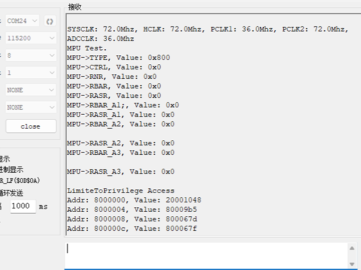
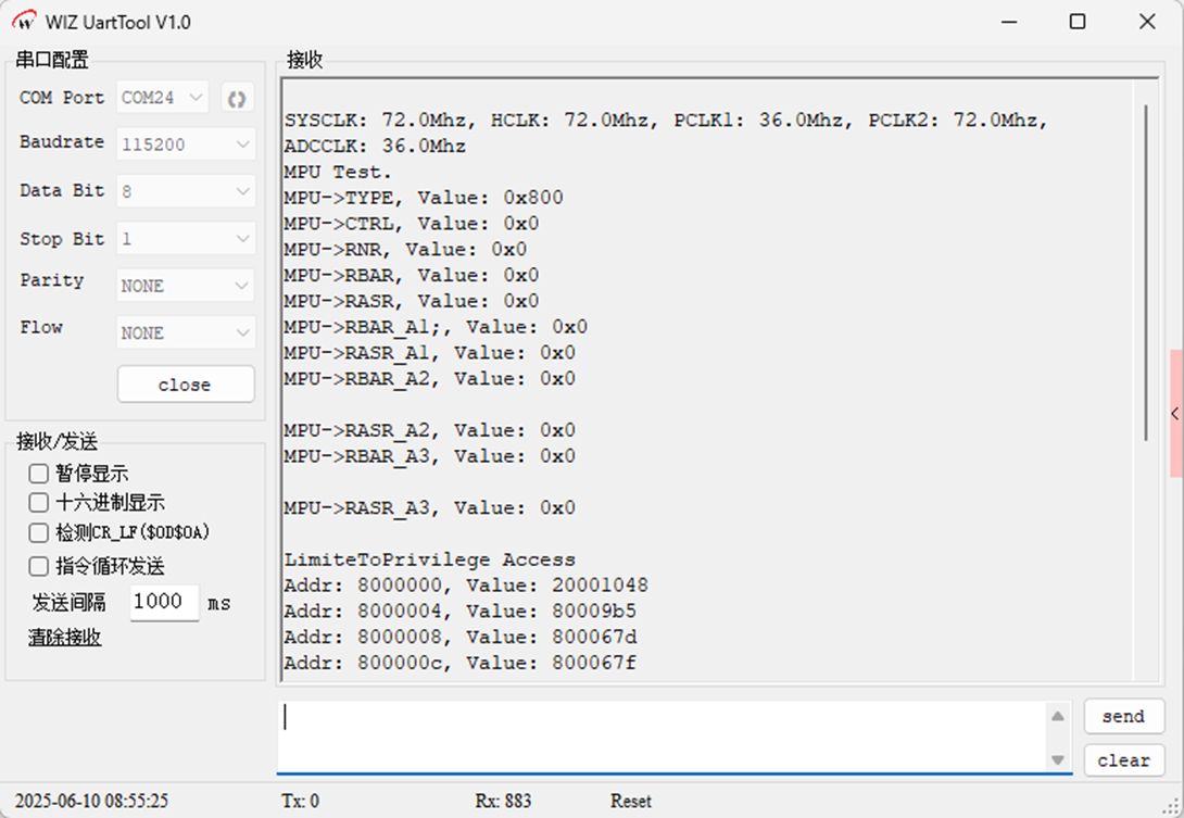
The main() function is the main program for the MPU functionality test: Firstly, it initializes the delay function and serial port (with a baud rate of 115200), calls the standard library to obtain the frequencies of each clock domain of the system (SYSCLK, HCLK, etc.) and prints them; then it prints the initial states of the MPU core registers (TYPE, CTRL, etc.) for debugging purposes;
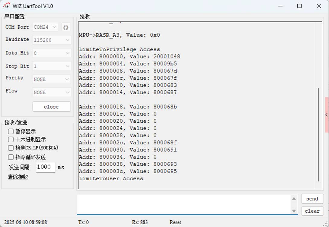
Subsequently, it calls MPU_Set to configure the memory protection rules, compares the access results of the first 64 bytes before and after the configuration (at the starting address of Flash, 0x08000000) in both privileged mode and user mode), to verify the effect of the MPU's restriction on memory access permissions; finally, it enters an infinite loop to keep running.
Download Verification
After the program was downloaded and run, it first printed the clock information, then the initial state information of the MPU's related registers, and then successfully accessed the memory with special permission restrictions. Subsequently, it was set for user access, and when accessed again, the content could not be read.
Summary
The MCO function enables W55MH32 to provide an external output clock by flexibly configuring the clock source and the division factor. This simplifies the clock synchronization issues in the system design. First, understand its application scenarios (such as multi-chip synchronization, debugging and measurement), and then master the configuration steps (clock source selection, GPIO setting, division configuration). This can be applied more efficiently in actual projects.
WIZnet is a non-chipfoundry semiconductor company founded in 1998. Its products include the Internet processor iMCU™, which adopts TOE (TCP/IP offloading engine) technology and is based on a unique patented fully hardwired TCP/IP. iMCU™ is designed for embedded Internet devices in various applications.
WIZnet has over 70 distributors worldwide, with offices in Hong Kong, South Korea, and the United States, providing technical support and product marketing.
The region managed by the Hong Kong office includes: Australia, India, Turkey, and Asia (excluding South Korea and Japan).