
Chapter 29: W55MH32’s Reading and Writing Internal FLASH
Chapter 29: W55MH32’s Reading and Writing Internal FLASH
Chapter 29: W55MH32’s Reading and Writing Internal FLASH
1 Introduction to the Internal FLASH of W55MH32
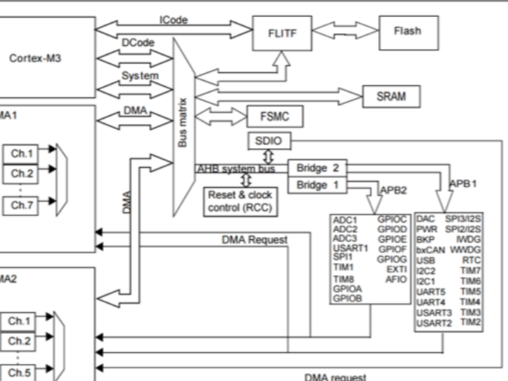
Inside the W55MH32 chip, there is a FLASH memory. It is mainly used for storing code. After we write the application program on the computer, we use the downloader to burn the compiled code file into this internal FLASH. Since the content of the FLASH memory will not be lost after power loss, when the chip is powered on and reset, the core can load the code from the internal FLASH and run it. See the following figure, the internal framework diagram of W55MH32:
Apart from using external tools (such as downloaders) to read and write the internal FLASH, the W55MH32 chip can also read and write its own internal FLASH while it is running. Therefore, if the internal FLASH has remaining space after storing the application program, we can utilize it like the external SPI-FLASH to store some data generated during the program's operation that needs to be saved after power-off.
Since the speed of accessing the internal FLASH is much faster than that of the external SPI-FLASH, in emergency situations, the internal FLASH is often used to store critical records. To prevent the application from being copied, some applications will prohibit reading and writing the content in the internal FLASH, or calculate and record the encryption information during the first run and then delete some of the encrypted code. All these applications involve the operation of the internal FLASH.
1.1 The composition of the internal FLASH
The internal FLASH of W55MH32 includes the main memory, system memory and option byte area. Their addresses and sizes are shown in the following table. The composition of the large-capacity W55MH32 product's internal FLASH:
Module | Name | Address | Size |
Main storage block | Page 0 | 0x0800 0000 - 0x0800 07FF | 2K |
| Page 1 | 0x0800 0800 - 0x0800 0FFF | 2K |
| Page 2 | 0x0800 1000 - 0x0800 17FF | 2K |
| Page 3 | 0x0800 1800 - 0x0800 1FFF | 2K |
| … | … | … |
| Page 255 | 0x0807 F800 - 0x0807 FFFF | 2K |
Information block | System memory | 0x1FFF F000 - 0x1FFF F7FF | 2K |
| Select bytes | 0x1FFF F000 - 0x1FFF F7FF | 16 |
Flash memory interface register | FLASH_ACR | 0x4002 2000 - 0x4002 2003 | 4 |
| FALSH_KEYR | 0x4002 2004 - 0x4002 2007 | 4 |
| FLASH_OPTKEYR | 0x4002 2008 - 0x4002 200B | 4 |
| FLASH_SR | 0x4002 200C - 0x4002 200F | 4 |
| FLASH_CR | 0x4002 2010 - 0x4002 2013 | 4 |
| FLASH_AR | 0x4002 2014 - 0x4002 2017 | 4 |
| Maintain | 0x4002 2018 - 0x4002 201F | 4 |
| FLASH_OBR | 0x4002 201C - 0x4002 201F | 4 |
| FLASH_WRPR | 0x4002 2020 - 0x4002 2023 | 4 |
Main memory
Model number | W55MH32L | W55MH32Q |
Flash (KB) | 1024 | 1024 |
SRAM (KB) | 96 | 96 |
Timer |
|
|
Advanced | 2 | 2 |
General | 10 | 10 |
Basic | 2 | 2 |
Communication interface |
|
|
SPI | 2 | 2 |
I2C | 2 | 2 |
USART/UART | 5 | 3 |
USB | 1 | 1 |
CAN | 1 | 1 |
SDIO | 1 | - |
Ethernet | 1 | 1 |
GPIO Port | 66 | 36 |
12-bit ADC (number of channels) | 3 (12 channels) | 3 (12 channels) |
12-bit DAC (number of channels) | 2 (2 channels) | 2 (2 channels) |
Random Number Module | Support | Support |
Hardware encryption algorithm unit | Support | Support |
Page size (K bytes) | 4 | 4 |
CPU frequency | 216M | 216M |
Working voltage | 2.0-3.6V | 2.0-3.6V |
Working temperature | -40-+85℃ | -40-+85℃ |
System storage area
The system storage area is an area that users cannot access. It has already been pre-programmed with the boot code when the chip was manufactured. This area is responsible for implementing ISP burning functions such as serial port, USB and CAN.
Option byte
The option bytes are used to configure functions such as read/write protection of FLASH, standby/shutdown reset, software/hardware watchdog, etc. This part consists of 16 bytes. These can be modified by changing the option control register of FLASH.
2 The writing process of the internal FLASH
2.1 Unlock
Since the internal FLASH space mainly stores the application programs, which are very crucial data, to prevent accidental modification of these contents, the chip will lock the control register FLASH_CR by default after reset. At this time, it is not allowed to set the FLASH control register, thus the contents in the FLASH cannot be modified.
2.2 Page erasure
Before writing new data, the storage area needs to be erased first. The W55MH32 provides page (sector) erase instructions and instructions for erasing the entire FLASH (batch erase). The batch erase instruction is only for the main storage area.
The process of page erasure is as follows:
(1) Check the "Busy Register Bit BSY" in the FLASH_SR register to confirm that no Flash operation is currently being executed;
(2) In the FLASH_CR register, set the "Activate Page Erase Register Bit PER" to 1;
(3) Use the FLASH_AR register to select the page to be erased;
(4) Set the "Start Erase Register Bit STRT" in the FLASH_CR register to 1 to start the erase process;
(5) Wait until the BSY bit is cleared, indicating that the erase operation is complete.
2.3 Writing Data
After erasure is completed, data can be written. The process of writing data is not merely assigning values to the address using a pointer; before the assignment, a series of registers need to be configured. The steps are as follows:
(1) Check the BSY bit in FLASH_SR to confirm that no other internal Flash operations are currently being executed;
(2) Set the "Activate Programming Register Bit PG" in FLASH_CR to 1;
(3) Perform a data write operation to the specified FLASH memory address, and each write can only be done in 16-bit increments;
(4) Wait until the BSY bit is cleared, indicating that the write operation is complete.
3 Examine the spatial distribution of the project
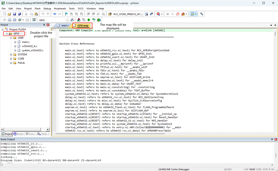
Since the internal FLASH itself stores program data, if one does not intentionally delete a certain section of program code, generally one should not modify the content of the program space. Therefore, before using the internal FLASH to store other data, it is necessary to understand which spaces have already been written with program code. The sectors that store program code should not be modified in any way. By querying the "*.map" suffix file generated during the application program compilation, one can understand which areas the program is stored in. The opening method of the project in the figure below can be seen. Open the map file of the project, or you can find it in the "Listing" folder in the project directory. For detailed explanations of the map file, please refer to the previous chapter "The Compilation Process and File Details of MDK".
3.1 The loading and execution space of the program ROM
There are two sections in the above description that start with "Load Region LR_ROM1" and "Execution Region ER_IROM1", respectively. These sections describe the loading and execution spaces of the program. When the chip is powered on and starts running, the program and data will be loaded, for example, it will load the program from the program storage area to the program execution area, and also copy some initialized global variables from ROM to RAM space so that the program can modify the content of the variables during execution. After the loading is completed, the program starts to execute from the execution area.
In the description of the above map file, we learned that the base addresses (Base) of the loading and execution spaces are both 0x08000000, which is exactly the starting address of the internal FLASH of W55MH32, that is, the program storage space of W55MH32 is directly the execution space; their sizes (Size) are 0x000017a8 and 0x0000177c respectively. The reason why the ROM of the execution space is relatively small is that some RW-data type variables have been copied to the RAM space; their maximum space (Max) is both 0x00080000, that is, 512K bytes, which refers to the maximum space of the internal FLASH.
When calculating the space occupied by the program, the size of the loading area needs to be used for calculation. In this example, the internal FLASH used by the application program is the space area from 0x08000000 to (0x08000000 + 0x000017a8) addresses.
3.2 ROM space distribution table
After loading and executing the overall description of the space, immediately following is a detailed ROM address distribution table. It lists the base addresses (BaseAddr) and the occupied space sizes (Size) of each segment (such as functions, constant data) in the project. The Type in the list indicates the type of the segment, CODE for code, DATA for data, and PAD for the padding area between segments, which is invalid content. The PAD area is often used to solve the problem of address alignment.
Looking at the last item in the table, its base address is 0x0800175c and its size is 0x00000020. It can be known that the highest address space it occupies is 0x0800177c, which is the same as the highest address of the execution area, 0x0000177c. However, they are smaller than the highest address stated in the loading area, 0x80017a8. Therefore, we take the size of the loading area as the standard. Comparing it with the internal FLASH page address distribution table of the W55MH32 large-capacity product, it can be seen that only pages 0 to 2 are sufficient to completely store this application program. Therefore, the storage space after page 3 (address 0x08001800) can be used for other purposes, and the data in these storage spaces will not be tampered with when using them.
4 Library functions for operating the internal FLASH
To simplify programming, the W55MH32 standard library provides some library functions that encapsulate the process of writing data to the internal FLASH memory operation registers.
4.1 FLASH unlocking and locking functions
The functions for unlocking and locking the internal FLASH are shown in the code listing: FLASH-2:
Code Listing: FLASH-2 FLASH Unlocking and Locking
#define FLASH_KEY1 ((uint32_t)0x45670123)When unlocking, it writes two unlocking parameters to the FLASH_KEYR register. When locking, it sets the FLASH_CR_LOCK bit in the FLASH_CR register to 1.
4.2 Setting the number of operation bits and page erasure
When erasing the sectors after unlocking, FLASH_EraseSector can be called to accomplish this task. Please refer to the code listing: FLASH-3:
Code Listing: FLASH-3 Erase Sector
/**This function includes an input parameter for setting the address of the page to be erased, which is the starting address of the target page in the internal FLASH. After obtaining the address, the function checks the status bits according to the previous process, writes the parameters to the control register FLASH_CR and the address register FLASH_AR, configures the start of the erase operation, and then waits for a period of time. The FLASH_WaitForLastOperation() function is used in the code to wait until the erase operation is completed before exiting the FLASH_EraseSector() function.
4.3 Write data
Writing data to the internal FLASH is not as straightforward as with SDRAM operations. Pointer operations alone do not suffice; a series of registers need to be set. Using the FLASH_ProgramWord() and FLASH_ProgramHalfWord() functions, data can be written in units of bytes or half-words. See the code listing: FLASH-4:
Code listing: FLASH-4 Writing data
/**
From the function code, it can be understood that after setting the PG bit of the FLASH->CR register to allow writing, a 16-bit pointer is used to write data to the specified address. Since each write operation can only be performed in 16-bit increments, this process of writing in bytes uses two pointer assignments, writing the low 16 bits and high 16 bits of the specified data respectively. After each assignment operation, the FLASH_WaitForLastOperation() function is called to wait for the write operation to complete. The standard library also provides the FLASH_ProgramHalfWord() function for writing half a word, which is 16 bits. The internal execution process of this function is similar.
5 Read and write the internal FLASH
5.1 Code analysis
- Macro definition
Address selection: Ensure that the selected address is not occupied by the program code and is within the erasable area
- Main function logic
int main(void)Infinite loop: Continuously test until the number overflows.
3. FLASH Erase and Programming Functions
void FLASH_EraseProgram(uint32_t number)Erase operation: Use FLASH_ErasePage to erase an entire page (usually 2KB).
Programming operation: Write 0x5A5A to each half-word, and verify the correctness of the write.
4. Time Measurement Function
void SYSTICK_Reset(void)Time calculation: The operation time (in clock cycles) is obtained by subtracting SysTick->VAL from 0xFFFFFF.
5. Serial port configuration function
void UART_Configuration(uint32_t bound)Function: Configure USART1 to operate at a baud rate of 115200 for debugging output.
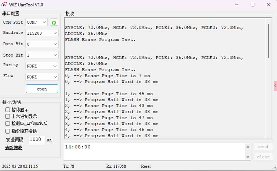
5.2 Download verification
6 FLASH_Eeprom
6.1 Code analysis
1. Main function main()
int main(void) {- Serial port configuration: UART_Configuration
void UART_Configuration(uint32_t bound) {Configure USART1 for outputting debugging information.
- Serial port redirection
int SER_PutChar(int ch) {4. FLASH Operation
This operation relies on WIZFLASH_Write and WIZFLASH_Read from eeprom.h. It is necessary to ensure that their implementations can perform the underlying operations of FLASH (erase, read/write, etc.).
Address: FLASH_SAVE_ADDR 0X08008000, which should be within the available FLASH space.
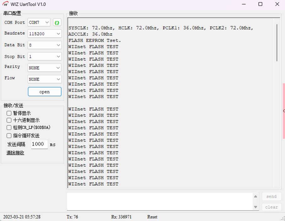
6.2 Download verification
WIZnet is a fabless semiconductor company founded in 1998. Its products include the Internet processor iMCU™, which utilizes TOE (TCP/IP Offload Engine) technology and is based on a unique patented fully hardwired TCP/IP. The iMCU™ is designed for embedded Internet devices in various applications.
WIZnet has more than 70 distributors globally and has offices in Hong Kong, South Korea, and the United States, providing technical support and product marketing services.
The regions managed by the Hong Kong office include Australia, India, Turkey, and Asia (excluding South Korea and Japan).