
Chapter 27: W55MH32’s Power Management - Achieving Low Power Consumption
Chapter 27: W55MH32’s Power Management - Achieving Low Power Consumption

Chapter 27: W55MH32’s Power Management - Achieving Low Power Consumption
References for this chapter: "W55MH32 Reference Manual".
1 Introduction to Power Management for W55MH32
The importance of power supply to electronic devices is self-evident. It is the foundation for ensuring the stable operation of the system. Once the system can operate stably, there is also a requirement for low power consumption. In many application scenarios, the power consumption requirements for electronic devices are extremely strict. For example, some sensor information collection devices rely solely on small batteries for power supply, and they are required to operate for several years without any maintenance. Due to the miniaturization requirements of smart wearable devices, the battery volume cannot be too large, resulting in a relatively small capacity. Therefore, it is also necessary to start from controlling power consumption to increase the running time of the device. Thus, the W55MH32 has a dedicated power management peripheral to monitor the power supply and manage the operating mode of the device, ensuring the normal operation of the system and minimizing the power consumption of the components.
1.1 Power monitor
The W55MH32 chip mainly obtains power from the external through pin VDD. Inside it, there is a power monitor which is used to detect the voltage of VDD, to achieve the reset function and the emergency power-off handling function, ensuring the reliable operation of the system.
1.1.1 Power-on Reset and Power-Off Reset (POR and PDR)
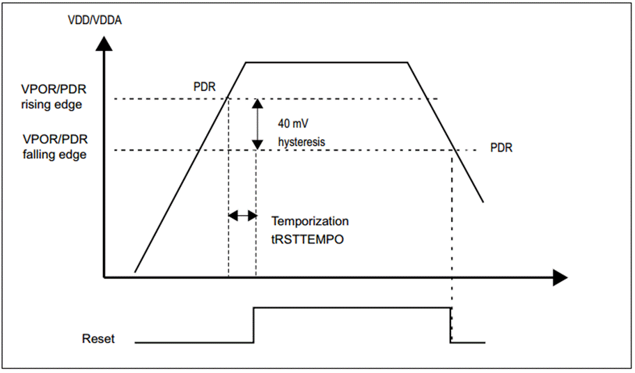
When the voltage of VDD is lower than the thresholds VPOR and VPDR, without the need for external circuit assistance, the W55MH32 chip will automatically remain in the reset state to prevent serious consequences caused by forced operation due to insufficient voltage. See the figure below, POR and PDR. At the beginning, when the voltage is lower than VPOR (approximately 1.92V), the W55MH32 remains in the power-on reset state (POR, Power On Reset). When the VDD voltage continuously rises to be greater than VPOR, the chip starts to operate normally. While the chip is operating normally, when the detected VDD voltage drops to be lower than the VPDR threshold (approximately 1.88V), it enters the power-down reset state (PDR, Power Down Reset).
1.1.2 Programmable Voltage Detector (PVD)
The above POR (Power On Reset) and PDR (Power Down Reset) functions work by comparing their voltage thresholds with the external supply voltage VDD. When the voltage is below the operating threshold, they will directly enter the reset state, which can prevent erroneous operations caused by insufficient voltage. In addition, the W55MH32 also provides a programmable voltage detector (PVD), which also detects the voltage of VDD in real time. When it detects that the voltage is below the programmed VPVD threshold, it will generate a PVD interrupt (EXTI16 line interrupt) to enable the kernel to perform emergency processing before the reset. The voltage threshold can be set through the power control register PWR_CSR.
The PVD can be configured with 8 levels, as shown in the table below, PVD's threshold levels. The rising edge and falling edge respectively represent the threshold values of the VDD voltage rising process and falling process as shown in POR and PDR in the figure.
Threshold level | Conditions | Minimum value | Typical value | Maximum value | Organization |
Level 0 | Rising edge | 2.1 | 2.18 | 2.26 | V |
Level 0 | Rising edge | 2 | 2.08 | 2.16 | V |
Level 1 | Rising edge | 2.19 | 2.28 | 2.37 | V |
Level 1 | Rising edge | 2.09 | 2.18 | 2.27 | V |
Level 2 | Rising edge | 2.28 | 2.38 | 2.48 | V |
Level 2 | Rising edge | 2.18 | 2.28 | 2.38 | V |
Level 3 | Rising edge | 2.38 | 2.48 | 2.58 | V |
Level 3 | Rising edge | 2.28 | 2.38 | 2.48 | V |
Level 4 | Rising edge | 2.47 | 2.58 | 2.69 | V |
Level 4 | Rising edge | 2.37 | 2.48 | 2.59 | V |
Level 5 | Rising edge | 2.57 | 2.68 | 2.79 | V |
Level 5 | Rising edge | 2.47 | 2.58 | 2.69 | V |
Level 6 | Rising edge | 2.66 | 2.78 | 2.9 | V |
Level 6 | Rising edge | 2.56 | 2.68 | 2.8 | V |
Level 7 | Rising edge | 2.76 | 2.88 | 3 | V |
Level 7 | Rising edge | 2.66 | 2.78 | 2.9 | V |
1.2 Power system of W55MH32
To facilitate power management, the W55MH32 has divided its peripheral, core and other modules into power supply areas based on their functions. The internal power supply area division of the W55MH32 is shown in the following figure. The power system of the W55MH32 :
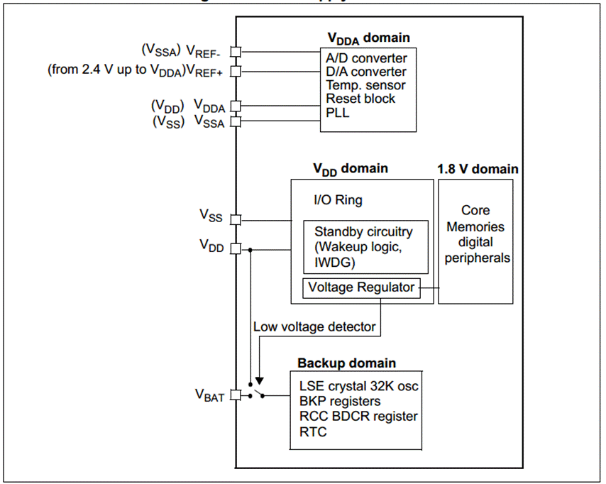
From the block diagram, it can be seen that the power system of W55MH32 is mainly divided into three parts: the backup domain circuit, the core circuit, and the ADC circuit. The details are as follows:
ADC power supply and reference voltage (VDDA power supply area)
To enhance the conversion accuracy, the ADC of W55MH32 is equipped with an independent power interface, facilitating separate filtering. The working power supply of the ADC is input through the VDDA pin, with VSSA serving as the independent ground connection, and the VREF pin providing the reference voltage for the ADC's measurement.
Pressure regulator power supply circuit (VDD/1.8V power supply area)
In the power system at W55, H32, the circuit powered by the voltage regulator is the most crucial part. The voltage regulator supplies power to all digital circuits except for the backup domain and the standby circuit, including the core, digital peripherals, and RAM. The output voltage of the voltage regulator is approximately 1.8V, so the circuit areas powered by the voltage regulator are called the 1.8V domain.
The voltage regulator can operate in "running mode", "stop mode", and "standby mode". In running mode, the 1.8V domain operates at full power; in stop mode, the 1.8V domain operates in a low-power state, all clocks in the 1.8V area are turned off, and all corresponding peripherals stop working, but it retains the contents of the core registers and SRAM; in standby mode, the entire 1.8V domain is powered off, and the contents of the core registers and SRAM in this area will be lost (the registers in the backup area are not affected).
Backup domain circuit (backup power supply area)
The LSE oscillator, RTC and backup registers of W55MH32 are incorporated into the backup domain circuit. This part of the circuit can obtain the power supply through the VBAT pin of W55MH32. In practical applications, a 3V button battery is usually used to supply power to this pin.
On the left side of the backup domain circuit in the figure, there is a power switch structure. Its function is similar to the double diode structure in the figure. At "1", it is connected to the VBAT power supply, at "2", it is connected to the VDD main power supply (generally 3.3V), and at "3" on the right, it is led out to the backup domain circuit. When the VDD main power supply exists, since the VDD voltage is higher, the backup domain circuit is powered by VDD, saving the power of the button battery, and only when the VDD power supply fails, the backup domain circuit is powered by the button battery through VBAT to ensure the circuit can continue to operate, thereby allowing it to retain critical data.
1.3 Power consumption mode of W55MH32
Arranged in descending order of power consumption, the W55MH32 has four working modes: operation, sleep, stop and standby. After power-on reset, when the core does not need to continue running, it can choose to enter the following three low-power modes to reduce power consumption. Among these three modes, the power consumption is different, the wake-up time is different, and the wake-up source is different. Users need to select the best low-power mode according to the application requirements. The descriptions of the three low-power modes are shown in the following table. The description of the low-power mode of W55MH32:
Mode | Explanation | Entry method | Wake-up method | The influence on the 1.8V system clock | The influence on the VDD area clock | Pressure regulator |
Sleep | The kernel has stopped, but all peripheral devices (such as NVIC, SysTick, etc.) are still operating. | Call the WFI command Call the WFE command | Any interruption Wakeup event | The internal clock is turned off, and this has no effect on other clocks and the ADC clock. | No | Open |
Stop | All clocks stopped. | Configure the PWR_CR register with the PDDS + LPDS + SLEEPDEEP bits + the WFI/WFE command | Any external interrupt (set in the external interrupt register) | Turn off all the clocks in the 1.8V area | HSI and HSE oscillators have been shut down. | Enable or enter low-power mode (depending on the setting of the power control register) |
Standby | 8V power supply turned off | Configure the PDDS + SLEEPDEEP bits in the PWR_CR register along with the WFI/WFE command. | WKUP pin rising edge, RTC alarm event, NRST external reset, IWDG reset | - | - | No
|
As can be seen from the table, these three low-power modes are successively more and more refined. The operating clock or chip functions become fewer and fewer, and thus the power consumption becomes lower and lower.
1.3.1 Sleep mode
In the sleep mode, only the kernel clock is turned off, and the kernel stops running, but all the on-chip peripherals of the core, the CM3 core's peripherals, continue to operate as usual. There are two ways to enter the sleep mode, and the way of entering determines the way of waking up from sleep, which are WFI (wait for interrupt) and WFE (wait for event), that is, waking up by waiting for an "interrupt" and by an "event". The various characteristics of the sleep mode are shown in the following table, the various characteristics of the sleep mode:
Characteristics | Explanation |
Go to sleep immediately | Enter the sleep mode immediately when executing the WFI or WFE instructions. |
Going into sleep upon exiting | The sleep mode is entered only after the interrupt service routine with the lowest priority has been exited. |
Entry method | The kernel register SLEEPDEEP is set to 0, and then by calling the WFI or WFE instructions, the system can enter the sleep mode; In addition, if the kernel register SLEEPONEXIT is 0, it enters the "immediate sleep" mode; when SLEEPONEXIT is 1, it enters the "sleep upon exit" mode. |
Wake-up method | If the sleep is achieved using the WFI instruction, any interrupt can be used to wake it up; If the sleep is achieved using the WFE instruction, it will be awakened by an event. |
During sleep | Turn off the kernel clock. The kernel stops, while the peripherals continue to operate normally. On the software side, it appears that no new code is being executed. This state retains the kernel registers and the data in the memory before the sleep. |
Awakening delay | No delay. |
After awakening | If awakened by an interrupt, it first enters the interrupt state, then exits the interrupt service program, and subsequently executes the program following the WFI instruction; if awakened by an event, it directly proceeds to execute the program after the WFE instruction. |
1.3.2 Stop mode
In the stop mode, all other clocks were further shut down, so all peripherals stopped working. However, since part of the power supply in its 1.8V area was not turned off, the kernel's registers and memory information were still retained. Therefore, when awakened from the stop mode and the clocks were restarted, the code could continue from where it left off the last time it was stopped. The stop mode can be awakened by any external interrupt (EXTI). In the stop mode, the voltage regulator can be set to either the normal mode or the low-power mode. The various characteristics of the stop mode are shown in the following table: Various characteristics of the stop mode:
Characteristics | Explanation |
Low power consumption mode of the pressure regulator | In the stop mode, the voltage regulator can operate in either normal mode or low-power mode, further reducing power consumption. |
Entry method | The SLEEPDEEP of the kernel register is set to 1, and the PDDS in the PWR_CR register is 0. Then, by calling the WFI or WFE instruction, the system can enter the stop mode; When the LPDS in the PWR_CR register is 0, the voltage regulator operates in the normal mode; when LPDS is 1, it operates in the low-power mode. |
Wake-up method | If the sleep is achieved using the WFI instruction, any EXTI line can be used for interrupt wake-up; If the sleep is achieved using the WFE instruction, any EXTI line configured in event mode can be used for event-based wake-up. |
Stop! | The kernel stops, and the on-chip peripherals also stop. This state will retain the kernel registers and the data in the memory before the stop. |
Awakening delay | The base delay is the startup time of the HSI oscillator. If the voltage regulator is operating in the low-power mode, it is also necessary to add the time it takes for the regulator to switch from the low-power mode to the normal mode. |
After awakening | If awakened by an interrupt, it first enters the interrupt state, then exits the interrupt service program, and subsequently executes the program following the WFI instruction; if awakened by an event, it directly proceeds to execute the program after the WFE instruction. After being awakened, HSI will be used as the system clock. |
1.3.3 Standby Mode
Standby mode. Besides shutting down all the clocks, it also completely turns off the power supply in the 1.8V area. That means, after waking up from standby mode, since there is no previous code execution record, the chip can only be reset and the boot condition needs to be re-detected. Then the program can be executed from the beginning. It has four wake-up methods, namely the rising edge of the WKUP (PA0) pin, the RTC alarm event, the reset of the NRST pin, and the IWDG (Independent Watchdog) reset.
Characteristics | Explanation |
Entry method | The kernel register SLEEPDEEP = 1, the PDDS bit in the PWR_CR register is 1, and the wake-up status bit WUF in the PWR_CR register is 0. Then, by calling the WFI or WFE instruction, the system can enter the sleep mode. |
Wake-up method | The RTC alarm, wake-up, intrusion, timestamp event or external reset via the NRST pin and IWDG reset can be awakened through the rising edge of the WKUP pin. |
When in standby mode | The kernel stops, and the on-chip peripherals also stop; the data in the kernel registers and in the memory will be lost; except for the reset pin, the RTC_AF1 pin and the WKUP pin, all other I/O ports operate in an open-drain state. |
Awakening delay | The time of chip reset |
After awakening | It is equivalent to a chip reset, where the program behaves as if it starts executing the code from the beginning. |
In the sleep mode, stop mode and standby mode described above, if the power supply of the backup domain is normal, the RTCs within the backup domain can operate normally, and the data of the registers within the backup domain will be saved and will not be affected by the power-saving mode.
2. Library functions and commands related to power management
The W55MH32 standard library provides comprehensive functions and commands for power management. By using these, control can be carried out conveniently. This section will explain these contents.
2.1 Configure the PVD monitoring function
PVD can monitor the voltage of VDD. When it drops below the threshold, it will generate a PVD interrupt to prompt the system to perform emergency handling. This threshold can be directly configured using the library function PWR_PVDLevelConfig to the threshold level as described in the table "PVD Threshold Levels" mentioned earlier.
2.2 WFI and WFE Commands
We have learned that when entering various low-power modes, the WFI or WFE commands need to be invoked. These commands are essentially kernel instructions. In the library file core_cm3.h, these instructions have been encapsulated into functions. Please refer to the code listing: Power Management - 1
Code Listing: Power Management - Definition of WFI and WFE Instructions (core_cm3.h file)
/** brief Wait for interruption For these two instructions, when we apply them, we generally only need to know that calling them will enable the low-power mode. The functions need to be invoked using the format "__WFI();" and "__WFE();" (because "__wfi" and "__wfe" are built-in functions of the compiler, and the functions internally call the corresponding assembly instructions). The WFI instruction determines that it needs to be awakened by an interrupt, while the WFE instruction determines that it can be awakened by an event. For more detailed differences between them, you can refer to "Cortex-CM3/CM4 Official Guide" for understanding.
2.3 Enter the stop mode
Directly invoking the WFI and WFE instructions can enter the sleep mode, while entering the stop mode requires setting certain register bits before invoking the instructions. The W55MH32 standard library encapsulates this operation in the PWR_EnterSTOPMode function, and its definition can be found in the code listing: Power Management - 2.
/**Code Listing: Power Management - 2 Entering Shutdown Mode
This function has two input parameters, which are used to control the mode of the voltage regulator and to select whether to use WFI or WFE to stop. In the code, the PWR_CR register is first configured according to the mode of the voltage regulator, and then the SLEEPDEEP bit of the kernel register is set to 1. Thus, when the WFI or WFE command is called, W55MH32 is not in sleep mode but enters the stop mode. The statement at the end of the function is used to reset the state of the SLEEPDEEP bit. Since it is after the WFI and WFE instructions, this part of the code will only be executed when W55MH32 is awakened.
It should be noted that after entering the stop mode, all I/O of W55MH32 remains in the state before the stop. When it is awakened, W55MH32 runs using HSI as the system clock (8 MHz). Since the system clock affects the working state of many peripherals, usually we will re-enable HSE and set the system clock back to its original state after waking up.
2.4 Enter standby mode
Similarly, the W55MH32 standard library also provides functions for controlling the entry into the standby mode. Their definitions can be found in the code listing: Power Management - 3
/**Code Listing: Power Management - 3 Enter Standby Mode
In this function, the PDDS register bits and the SLEEPDEEP register bits are first configured. Then, the __force_stores() function is called to ensure that the storage operations are completed before the WFI instruction is executed, thus entering the sleep mode. It is worth noting here that the sleep mode can also be entered using the WFE instruction. If you need to, you can modify it yourself.
After entering the sleep mode, all I/Os except those enabled for waking up enter a high-impedance state. And after waking up from the sleep mode, it is equivalent to resetting the W55MH32 chip, and the program starts executing from the beginning again.
3 PWR - Power Voltage Detection Function
3.1 Code Analysis
#include <stdlib.h>1. The header file includes the definitions of global variables.
It includes the header files of the standard library as well as the custom delay.h and w55mh32.h header files.
A pointer USART_TEST pointing to the USART_TypeDef structure is defined, and it is initialized as USART1 for subsequent serial port operations.
2. Function declaration
void UART_Configuration(uint32_t bound);Two functions are declared: UART_Configuration() is used for configuring serial communication, and PVD_Configuration() is used for configuring the power voltage detection (PVD) function.
3. The main() function
A variable of type RCC_ClocksTypeDef named "clocks" was defined to store the system clock frequency information.
int main(void)
{The delay_init() function was called to initialize the delay functionality.
The UART_Configuration() function was called to configure the serial communication with a baud rate of 115200.
The RCC_GetClocksFreq() function was called to obtain the system clock frequency information and print it out via the serial port.
The PVD_Configuration() function was called to configure the power voltage detection function.
An infinite loop was entered to keep the program running.
4. PVD_Configuration() Function
void PVD_Configuration(void)Variables of the types EXTI_InitTypeDef and NVIC_InitTypeDef were defined, which are used to configure the external interrupt and the Nested Vectored Interrupt Controller (NVIC).
Enable the clocks of the PWR (Power Control) and BKP (Backup Domain) peripherals.
Clear the interrupt pending flag of the external interrupt line 16.
Configure the external interrupt line 16 as an interrupt mode, with trigger types being rising edge and falling edge, and enable this interrupt line.
Configure the priority grouping of NVIC as 1.
Configure the priority of the PVD interrupt, and enable this interrupt.
Set the threshold of PVD to 2.9V, and enable the PVD function.
5. UART_Configuration() Function
void UART_Configuration(uint32_t bound)Variables of type GPIO_InitTypeDef and USART_InitTypeDef were defined, which were used to configure GPIO and USART respectively.
The clocks of USART1 and GPIOA were enabled.
Pin 9 of GPIOA was configured as a re-mapped push-pull output mode for the transmission function of USART1; pin 10 was configured as an open-drain input mode for the reception function of USART1.
The parameters such as baud rate, data bits, stop bits, and parity check of USART1 were configured, and USART1 was enabled.
6. PVD_IRQHandler() Function
void PVD_IRQHandler(void)Check whether the interrupt flag of external interrupt line 16 is set.
If the PVD output flag (PWR_FLAG_PVDO) is set, it indicates that the power voltage is lower than the set threshold. Output corresponding information through the serial port; otherwise, it indicates that the power voltage is higher than the set threshold, and also output corresponding information through the serial port.
Clear the interrupt suspend flag of external interrupt line 16.
7. The SER_PutChar() and fputc() functions
int SER_PutChar(int ch)The SER_PutChar() function is used to send a character to the serial port. It waits until the sending completion flag is set before sending the next character.
The fputc() function is the underlying implementation of the standard library function printf(), and it sends characters to the serial port. If a newline character \n is encountered, it first sends a carriage return character \r.
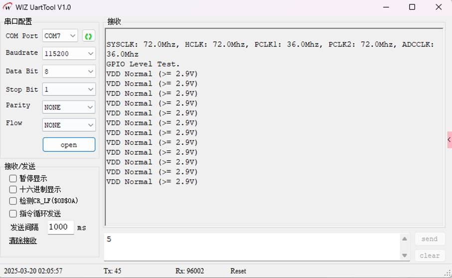
This code configures the PVD function to monitor the power voltage in real time. It triggers an interrupt when the voltage is above or below the set threshold. It outputs corresponding prompt information through the serial port. At the same time, it configures the serial communication function to output the system clock frequency information and the PVD monitoring results.
3.2 Download verification
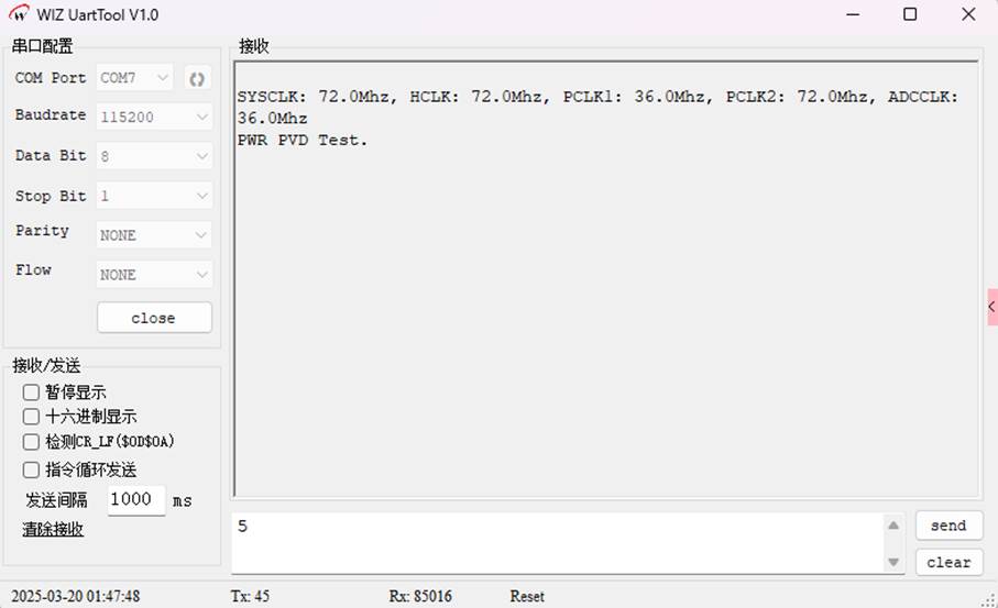
Under normal voltage conditions, it does not display. If you want to view it, you can add the code yourself; for example:
while (1)The display effect is as follows:
4 Standby and Wake-up
4.1 Code Analysis
1. Header files and global variables
#include <stdlib.h>It includes standard library header files and custom header files.
USART_TEST is a pointer to USART1, used for subsequent serial port operations.
2. Function declaration
void UART_Configuration(uint32_t bound);Three functions are declared:
UART_Configuration(): used for configuring the serial port.
GPIO_Configuration(): used for configuring GPIO pins.
GetCmd(): used for obtaining the user input command from the serial port.
3. The main function "main()"
int main(void)Clock and peripheral enablement:
RCC_APB1PeriphClockCmd(RCC_APB1Periph_PWR | RCC_APB1Periph_BKP, ENABLE); Enable the clocks for the power management peripheral (PWR) and backup registers (BKP).
Initialization operation:
delay_init(): Initialization delay function.
UART_Configuration(115200):
Configure the serial port baud rate to 115200.
RCC_GetClocksFreq(&clocks):
Obtain the system clock frequency information.
Information output:
Output the system clock frequency information through the printf() function and prompt the user that they can enter 's' to put the device into standby mode.
Wake-up pin enable:
PWR_WakeUpPinCmd(ENABLE): Enable the wake-up pin (PA0), which is used to wake up the device from the standby mode.
Wait for user input: while (GetCmd() ! = 's'); : Continuously wait for the user to input character s via the serial port.
GPIO configuration and entering standby mode:
GPIO_Configuration(): Configure all GPIO pins to analog input mode.
PWR_EnterSTANDBYMode(): Make the device enter standby mode.
Infinite loop: while (1);
Entering the infinite loop. In fact, this part will not be executed after entering the standby mode.
4. GPIO_Configuration() Function
void GPIO_Configuration(void)Enable the clock for all GPIO ports.
Configure the initialization structure for the GPIO pins, setting all pins to analog input mode with a speed of 50 MHz.
Initialize all GPIO pins for analog input mode for all GPIO ports through a loop and the GPIO_Init() function.
5. UART_Configuration() Function
void UART_Configuration(uint32_t bound)Enable the clocks for USART1 and GPIOA.
Configure PA9 as a re-mapped push-pull output (for USART1's transmission), and PA10 as an open-drain input (for USART1's reception).
Configure the parameters of USART1 such as baud rate, data bits, stop bits, parity check, etc., and enable USART1.
6.GetCmd() Function
uint8_t GetCmd(void)Check the non-empty flag of the receive buffer of USART1 (USART_FLAG_RXNE).
If the flag is set, it indicates that data has been received. The data is read from the receive buffer of USART1 and stored in the variable tmp, and then returned.
7. SER_PutChar() and fputc() functions
int SER_PutChar(int ch)The SER_PutChar() function is used to send a character to the serial port. It waits until the sending completion flag (USART_FLAG_TC) is set before sending the next character.
The fputc() function is the underlying implementation of the standard library's printf() function. When sending a newline character (\n), it first sends a carriage return character (\r) to ensure correct display on the serial port terminal.
The main function of this code is to allow users to input the "s" command through the serial port to put the W55MH32 device into standby mode, and enable the wake-up pin (PA0). This pin can be used to wake up the device in the standby mode. Before entering the standby mode, all GPIO pins are configured to the analog input mode to reduce power consumption. System clock frequency information and operation prompts can be output through the serial port.
4.2 Download Verification
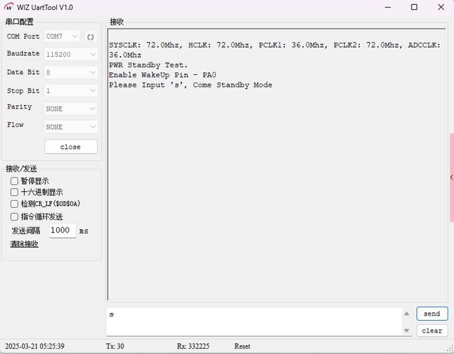
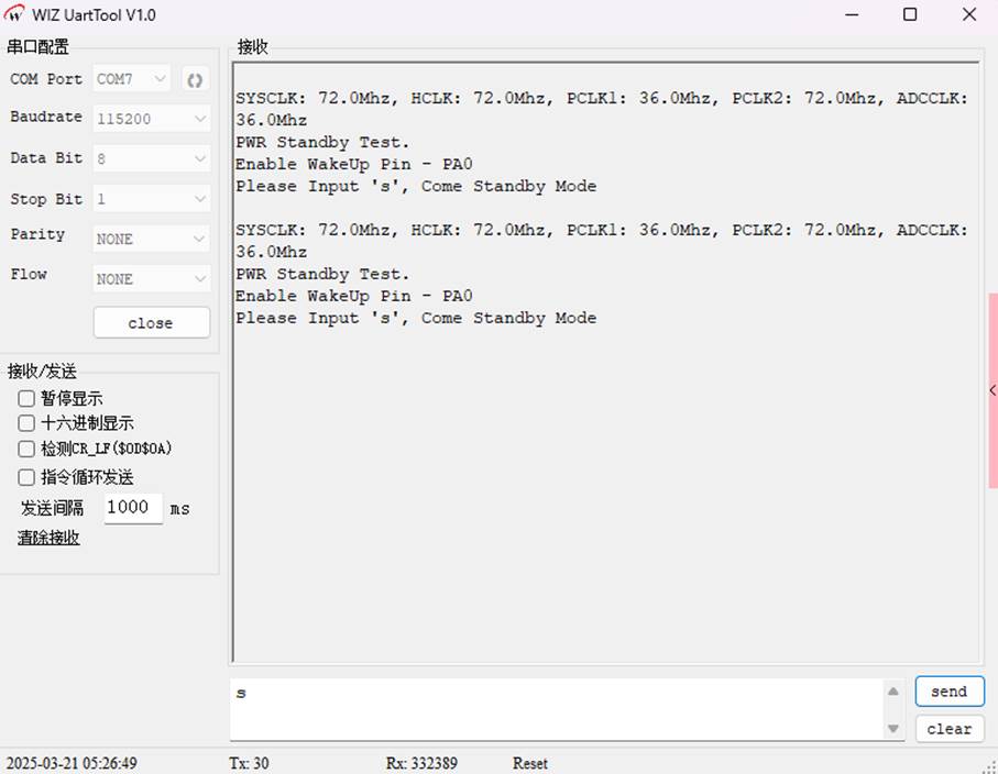
Input 's' has entered standby mode.
Pull up the PA0 pin to wake up the device:
WIZnet is a fabless semiconductor company founded in 1998. Its products include the Internet processor iMCU™, which utilizes TOE (TCP/IP Offload Engine) technology and is based on a unique patented fully hardwired TCP/IP. The iMCU™ is designed for embedded Internet devices in various applications.
WIZnet has more than 70 distributors globally and has offices in Hong Kong, South Korea, and the United States, providing technical support and product marketing services.
The regions managed by the Hong Kong office include Australia, India, Turkey, and Asia (excluding South Korea and Japan).