
Chapter 26:W55MH32 DAC - Output Sine Wave
Chapter 26:W55MH32 DAC - Output Sine Wave
Chapter 26:W55MH32 DAC - Output Sine Wave
References for this chapter: "W55MH32 Reference Manual" - DAC section.
When studying this chapter, it will be more effective to read it in conjunction with the DAC section of the "W55MH32 Reference Manual", especially for the part related to register descriptions.
1 Introduction to DAC
DAC is a digital/analog conversion module. As the name suggests, its function is to convert the input digital code into the corresponding analog voltage output. Its function is opposite to that of ADC. In common digital signal systems, most sensor signals are converted into voltage signals, and ADC converts the voltage analog signals into digital codes that are easy for computers to store and process. After being processed by the computer, the voltage analog signals are output by DAC. These voltage analog signals are often used to drive certain execution devices, making it easier for humans to perceive. For example, the acquisition and restoration of audio signals is such a process.
The W55MH32 has an on-chip DAC peripheral. Its resolution can be configured as 8-bit or 12-bit digital input signals. It has two DAC output channels, and these two channels do not affect each other. Each channel can use the DMA function and has error detection capability and can be triggered externally.
2 Analysis of the DAC Function Block Diagram
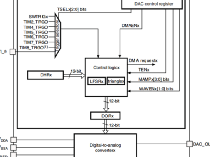
The block diagram of the DAC module of W55MH32 is as follows:
The entire DAC module is centered around the "Digital-to-Analog Converter x" at the bottom of the block diagram. On its left are the pins for the reference power supply: VDDA, VSSA, and VREF+. Among them, the DAC of W55MH32 specifies its reference voltage: the input range of math: V_{ref +} is 2.4 - 3.3V. The input of "Digital-to-Analog Converter x" is the digital encoding of the DAC's data register "DORx", and the analog signal obtained after conversion passes through it and is output by "DAC_OUTx" on the right side of the diagram. The data register "DORx" is controlled by the "Control Logic", which can control the addition of some pseudo-noise signals or the generation of triangular wave signals. The upper left corner of the diagram is the trigger source of the DAC. The DAC performs the DAC conversion based on the signal from the trigger source, and its function is equivalent to the switch of the DAC converter, which can be configured to trigger by external interrupt source, timer trigger, or software control trigger. As in the experiments of this chapter, if the frequency of the sine wave needs to be controlled, a timer will trigger the DAC for data conversion.
2.1 Reference voltage
Similar to the ADC peripheral, the DAC also uses the VREF+ pin as the reference voltage. When designing the schematic diagram, it is common to ground VSSA, connect VREF+ and VDDA to 3.3V, and the output voltage range of the DAC can be 0 to 3.3V.
If you want to widen the output voltage range, you can add an external voltage regulation circuit to lift the 0 to 3.3V DAC output to a specific range.
2.2 Digital-to-analog conversion and output channels
In the block diagram, "Digital-to-Analog Converter x" is the core component, and the entire DAC peripheral is arranged around it. It uses the VREF+ on the left as the reference power supply, and the digital encoding of the data register "DORx" of the DAC as the input. The analog signal obtained after conversion passes through it and is output through the "DAC_OUTx" channel on the right. In each component, the "x" refers to the device's serial number. In W55MH32, there are 2 such DAC components, and each DAC has a corresponding output channel connected to a specific pin, namely: PA4 - Channel 1, PA5 - Channel 2. To avoid interference, when using the DAC function, the DAC channel pins need to be configured as analog input function (AIN).
2.3 Trigger source and DHRx register
When using the DAC, data cannot be directly written to the aforementioned DORx register. Any data output to DAC channel x must be written to the DHRx register (which includes DHR8Rx, DHR12Lx, etc., written to the corresponding register based on the data alignment direction and resolution).
After the data is written to the DHRx register, the DAC will process it according to the trigger configuration. If a hardware trigger is used, the data in DHRx will be transmitted to DORx after 3 APB1 clock cycles, and DORx will then output the corresponding analog voltage to the output channel. If the DAC is set to external event triggering, the timing of data DAC conversion can be controlled using several methods such as timer (TIMx_TRGO), EXTI_9 signal, or software trigger (SWTRIGx). For example, using a timer trigger, combined with the data in DHRx at different times, the function of DAC outputting a sine wave can be achieved.
3 Detailed Explanation of the DAC Initialization Structure
In the W55MH32 standard library, various configurations related to controlling the DAC are encapsulated into the structure DAC_InitTypeDef. This structure mainly contains the configuration of each register bit of the DAC_CR control register. See code listing: DAC-1
Code Listing: DAC-1 DAC_InitTypeDef Structure
typedef struct {The descriptions of each structure member are as follows. In the explanations, the English in the parentheses after each mode is the macro used for that mode in the standard library:
DAC_Trigger
This member is used to configure the trigger mode of the DAC. The value of the DHRx register will only be transferred to the DORx register for conversion when the DAC generates the corresponding trigger event. The selectable trigger modes for this structure member are as follows: Hardware trigger mode (DAC_Trigger_None), where the data in the DHRx register will be automatically converted to DORx within 3 APB1 clock cycles for conversion; Timer trigger mode (DAC_Trigger_T2/4/5/6/7_TRGO), using timers 2, 4, 5, 6, and 7 to control the data in the DHRx register to be transferred to DORx at a certain time for conversion; EXTI_9 trigger mode (DAC_Trigger_Ext_IT9), triggering the conversion when an EXTI_9 event occurs (such as a GPIO interrupt event); Software trigger mode (DAC_Trigger_Software), in this mode, writing configuration to the DAC_SWTRIGR register can trigger the signal for conversion.
DAC_WaveGeneration
This member is used to set whether to use the DAC output for pseudo noise or triangle wave (DAC_WaveGeneration_None/Noise/Triangle). When using pseudo noise and triangle wave outputs, the DAC will add the value of the LFSR register to the DHRx value, generating pseudo noise and triangle wave. If you want to generate a custom output, simply configure it as DAC_WaveGeneration_None.
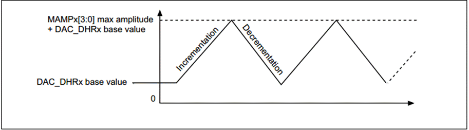
DAC_LFSRUnmask_TriangleAmplitude
This member sets the data of the LFSR register bits by controlling the MAMP2 bit of DAC_CR. That is, when using pseudo noise or triangular wave output, it should be superimposed onto the value of DHRx. In the non-noise or triangular wave output mode, this configuration is invalid. When using pseudo noise output, LFSR = 0xAAA, and the MAMP2 register bit can mask certain bits of the LFSR. At this time, simply assign the members of this structure to the macros such as DAC_LFSRUnmask_Bit0~DAC_LFSRUnmask_Bit11_0; when using triangular wave output, this structure sets the maximum amplitude of the triangular wave, which can be selected as DAC_TriangleAmplitude_1~DAC_TriangleAmplitude_4096 etc. as shown in the figure. The DAC outputs a triangular wave. The DAC rises based on the value of DHRx, and when the amplitude reaches the maximum amplitude set by MAMPx, it drops, forming the output of the triangular wave.
DAC_OutputBuffer
This structure member is used to control whether to enable the output buffer of the DAC (DAC_OutputBuffer_Enable/Disable). Once the output buffer of the DAC is enabled, the output impedance can be reduced, making it suitable for directly driving some external loads.
4 Experiment on Outputting Sine Wave by DAC
This code is written based on the W55MH32 microcontroller. Its main function is to output a dual-channel sine wave signal through the DAC (Digital-to-Analog Converter), and it is also configured with serial communication to output system clock information.
4.1 Code Analysis
1. Macro definitions and global variables
#define DAC1_DHR12RD_ADDRESS (DAC_BASE + 0x00000008 + DAC_Align_12b_R)DAC1_DHR12RD_ADDRESS and DAC2_DHR12RD_ADDRESS: These define the 12-bit right-aligned data register addresses for DAC1 and DAC2 respectively.
POINT_NUM: Defines the number of sampling points within one cycle of the sine wave, which is 32 points here.
Sine12bit: Stores the 12-bit sampling data of one cycle of the sine wave.
DualSine12bit: Is used to store the sine wave data for two channels.
2. Function declaration
void UART_Configuration(uint32_t bound);Declared the functions used for configuring the serial port, GPIO, DAC, timer and DMA.
3. The main() function
int main(void)Enable the CRC peripheral clock, initialize the delay function, configure the serial communication baud rate to 115200, and obtain the system clock frequency information.
Print the system clock frequency information and the test prompt information.
Call the GPIO_Configuration, DAC_Configuration() and TIM_Configuration() functions in sequence to configure GPIO, DAC and timer.
Convert the mono sine wave data to dual-channel data and store it in the DualSine12bit array.
Call the DMA_Configuration() function to configure the DMA transmission.
Enter an infinite loop to keep the program running.
4. DMA_Configuration() function
void DMA_Configuration(void)Enable the peripheral clock of DMA2.
Configure DMA2 channel 4 to transfer the dual-channel sine wave data from the memory to the data register of DAC2.
Configure DMA2 channel 3 to transfer the dual-channel sine wave data from the memory to the data register of DAC1.
Use the circular mode to make DMA continuously cycle and transfer data.
5. TIM_Configuration() Function
void TIM_Configuration(void)Enable the peripheral clock of Timer 2.
Configure the period of Timer 2 to be 20 clock cycles, with the prescaler set to 0 and the counter to count upwards.
Select the update event of Timer 2 as the trigger output.
Enable Timer 2.
6. GPIO_Configuration() function
void GPIO_Configuration(void)Enable the peripheral clock of GPIOA.
Configure pins 4 and 5 of GPIOA to be in analog input mode with a speed of 50 MHz.
7. DAC_Configuration() Function
void DAC_Configuration(void)Enable the DAC peripheral clock.
Configure the trigger sources of DAC channel 1 and channel 2 as the trigger output of Timer 2.
Do not generate waveforms, enable the output buffer.
Enable DAC channel 1 and channel 2, and enable DMA transmission.
8. UART_Configuration() Function
void UART_Configuration(uint32_t bound)Enable the peripheral clocks of USART1 and GPIOA.
Configure pin 9 of GPIOA as a re-mapped push-pull output, and pin 10 as an open-drain input.
Configure the parameters of USART1 such as baud rate, data bits, stop bits, parity check, etc.
Enable USART1.
9. SER_PutChar() and fputc() functions
int SER_PutChar(int ch)SER_PutChar(): Sends a character to the USART and waits for the transmission completion flag.
fputc(): Redirects the standard output function, sending characters to the USART. When encountering a newline character, it sends a carriage return character first.
In summary, this code achieves the output of dual-channel sine wave signals by configuring the timer, DMA, and DAC, and outputs the system clock information through the serial port.
WIZnet is a fabless semiconductor company founded in 1998. Its products include the Internet processor iMCU™, which utilizes TOE (TCP/IP Offload Engine) technology and is based on a unique patented fully hardwired TCP/IP. The iMCU™ is designed for embedded Internet devices in various applications.
WIZnet has more than 70 distributors globally and has offices in Hong Kong, South Korea, and the United States, providing technical support and product marketing services.
The regions managed by the Hong Kong office include Australia, India, Turkey, and Asia (excluding South Korea and Japan).